Abstract
A simple electrochemical deposition technique is used to synthesize both two-dimensional (nanowall) and one-dimensional (nanowire) ZnO nanostructures on indium-tin-oxide-coated glass substrates at 70°C. By fine-tuning the deposition conditions, particularly the initial Zn(NO3)2·6H2O electrolyte concentration, the mean ledge thickness of the nanowalls (50–100 nm) and the average diameter of the nanowires (50–120 nm) can be easily varied. The KCl supporting electrolyte used in the electrodeposition also has a pronounced effect on the formation of the nanowalls, due to the adsorption of Cl− ions on the preferred (0001) growth plane of ZnO and thereby redirecting growth on the (10 0) and (2
 0) planes. Furthermore, evolution from the formation of ZnO nanowalls to formation of nanowires is observed as the KCl concentration is reduced in the electrolyte. The crystalline properties and growth directions of the as-synthesized ZnO nanostructures are studied in details by glancing-incidence X-ray diffraction and transmission electron microscopy.
Keywords: ZnO nanostructures, Dimensional control, Electrodeposition, Electron microscopy
Introduction
ZnO-nanostructured films are one of the promising wide-band-gap (3.37 eV) semiconducting materials with a wide range of potential applications, including UV lasers, light emitting diodes, nanogenerators, transistors, sensors, catalysts, electron emitters, and solar cells [1,2]. The efficiency and performance of any optical and electrical nanodevices are directly determined by the properties of underlying nanostructures, which are in turn greatly dependent on the crystallographic orientation, size, shape, and morphology. The deposition techniques and their corresponding deposition parameters play an important role in controlling the morphology and physical properties of the nanostructures. Both physical deposition, including thermal evaporation, metalorganic chemical vapor deposition, pulsed laser deposition [3-5], and chemical synthetic routes, including hydrothermal, solvothermal, sol–gel, electrochemical, chemical bath deposition [6-15], have been successfully employed to prepare a wide variety of ZnO nanostructures. The physical deposition routes have the advantages of producing high-quality materials, but also the disadvantage of the need for high temperature and catalysts such as Sn [16], Au [17,18], Co [19], and NiO [20]. Although catalyst-free, single-step [21,22], and multi-step [23-26] physical deposition methods have been achieved recently to synthesize ZnO nanostructures, the required high growth temperature necessitates the use of expensive substrates such as sapphire and silicon. Unlike the physical deposition routes, wet-chemistry or solution-based approach has attracted renewed attention due to their low temperature, catalyst-free growth processes, which lead to the successful deposition of ZnO on inexpensive substrates, including glass [13,27-29] and plastics [30-33]. In addition, the wet-chemistry approach has strong potential in mass-scale production and deposition on large-area substrates. In the wet-chemistry approach, the concentrations and the components of the solutions play a major role in controlling the shape and size of ZnO nanostructures [34,35].
Of the several wet-chemistry methods, including hydrothermal, sol–gel techniques, and chemical bath deposition, that have been used to synthesize ZnO nanostructures, electrodeposition represents a versatile technique for producing nanostructures with easily controllable morphologies. Unlike other wet-chemistry approaches, electrodeposition requires the use of a conducting substrate, and therefore, it can be easily adapted for selected-area deposition of nanostructures by creating conducting patterns on the substrate. Moreover, electrodeposition offers other advantages, including a lower deposition temperature, a relatively short growth time, and more environment-friendly chemicals [13,29]. While electrodeposition of ZnO is normally carried out below 90°C, with a deposition time less than 2 h and in simple aqueous salt solutions [13], the hydrothermal method, for example, often requires a temperature of 60–200°C, a deposition time of 1 h to a few days [31,36], and less environment-friendly chemicals such as methenamine or diethylenetriamine [30,31,36]. Peulon et al. [13] and Izaki et al. [37] have pioneered the use of electrodeposition for growing ZnO films and other nanostructures. More recently, several studies have been conducted on the electrodeposition of ZnO thin films and nanostructures on conducting glass substrates [13,27-29]. However, there are only a limited number of detailed reports on the dimensional control of the length and diameter of ZnO nanowires [28,38], and no study is available on controlling the ledge thickness of nanowalls and indeed other similar kinds of two-dimensional (2D) ZnO nanostructures (such as nanoplatelets, nanosheets, and nanodisks).
In the past two decades, most of the nanomaterials research have primarily focused on zero-dimensional materials, particularly nanoparticles and quantum dots, and one-dimensional (1D) materials, such as nanowires, nanorods, and nanotubes. To date, only a limited number of studies have been carried out on 2D nanostructures [17,18,39-43]. In the present work, we demonstrate that electrodeposition can be used effectively to control the shape and size of the 2D (nanowalls) and 1D (nanowires) ZnO nanostructures. By carefully changing the electrolyte concentration, it is possible to produce nanowalls and nanowires with controllable ledge thicknesses and diameters, respectively. Furthermore, it has been recently confirmed that adsorption of Cl− ions on the preferred (0001) growth plane of ZnO is the underlying mechanism that drives the formation of 2D nanostructures [44-46] and of nanowires with increasing diameters [29]. In the present work, we also provide a detailed study on the effect of the supporting electrolyte (KCl) concentration on the structural transition from the formation of nanowalls to that of nanowires. The electrodeposited ZnO nanostructures are extensively characterized by scanning electron microscopy (SEM), glancing-incidence X-ray diffraction (GIXRD), and transmission electron microscopy (TEM).
Experimental Details
All the electrodeposition experiments were carried out in a three-electrode glass cell immersed in a water bath held at 70°C. A CH Instruments 660A electrochemical workstation was used for the nanostructure growth by amperometry potentiostatically at −1.1 V with respect to a Ag/AgCl reference electrode. An indium-tin-oxide (ITO)-coated glass substrate (with a sheet resistance of 4–8 Ω) was used as the working electrode with an exposed area of 10 × 5 mm2, while a Pt spiral wire served as the counter electrode. For the growth of ZnO nanowalls, a higher Zn(NO3)2·6H2O electrolyte concentration regime (0.1–0.2 M) was used, whereas nanowire growth employed a lower-concentration regime (0.0005–0.001 M). A KCl solution with a fixed concentration of 0.1 M was added as the supporting electrolyte to increase the conductivity. The deposition time was varied to control the film thickness of ZnO nanowalls and the length of ZnO nanowires. In another set of experiments, the Zn(NO3)2·6H2O concentration was kept constant at 0.1 M, while the KCl concentration was varied from 0.1 to 0.001 M in order to study the effect of Cl− ions on the growth evolution of ZnO nanowalls to nanowires. This result was also compared with that obtained with a second supporting electrolyte KNO3 (i.e., without Cl− ions). It should be noted that the concentrations mentioned above and used throughout the manuscript are the initial concentrations of the electrolyte. The actual concentration could change differently with deposition conditions as the electrodeposition proceeds with time. The morphology of resulting ZnO nanodeposits on the ITO–glass substrates and their corresponding film thickness were characterized using a LEO FESEM 1530 field-emission SEM. The microstructural properties of these ZnO-nanostructured films were analyzed using a PANalytical X’Pert Pro MRD XRD in glancing-incidence mode and a JEOL 2010 TEM operated at 200 kV.
Results and Discussion
Effect of Initial Electrolyte Concentration on the Morphology of ZnO Nanostructure
Figure 1 shows the typical SEM images of ZnO nanowalls electrochemically deposited on ITO–glass substrates at 70°C for 20 min at different Zn(NO3)2·6H2O initial concentrations in the range of 0.1–0.2 M (all with 0.1 M KCl). The insets show the overall homogeneity of the nanowall films at a lower magnification. At all the concentrations, the growth of nanowalls is found to be uniform and near-vertical, as indicated by the observation that only the top ledge surfaces of the nanowalls are revealed in the SEM images. A large fraction of the nanowalls is found to form local groups with a parallel arrangement. At Zn(NO3)2·6H2O concentrations of 0.2 and 0.175 M, the nanowall ledge surfaces appear to be more rough than those of the nanowalls obtained at lower concentrations of 0.15 and 0.125 M [as observed in the SEM images obtained at a higher magnification (not shown)]. The rougher ledge surface at a higher electrolytic concentration (0.175 or 0.2 M) could be due to faster reaction kinetics and formation of complex salts that are known to occur at a higher Zn2+ concentration [47]. Furthermore, the mean ledge thickness of nanowalls is found to decrease with the Zn(NO3)2·6H2O concentration. Figure 2 summarizes the changes in the mean ledge thickness of nanowalls and the film thickness as functions of the Zn(NO3)2·6H2O concentration and deposition time, respectively. The mean ledge thickness of nanowalls obtained at Zn(NO3)2·6H2O concentrations of 0.2, 0.175, 0.15, 0.125, and 0.1 M (for 20 min deposition time) are 88, 81, 70, 62, and 58 nm, respectively, which follows an almost linear trend (Fig. 2a). In another set of experiments, nanowalls deposition was carried out by changing the deposition time while keeping the Zn(NO3)2·6H2O concentration at 0.1 M, in order to measure the growth rate from the cross-sectional SEM images. Evidently, two regimes in the growth rate, marked with dashed lines, can be seen from the plot of film thickness versus deposition time (Fig. 2b). In the first 30 min of deposition, the growth rate is measured to be 1.36 μm/min, whereas a slower growth rate of 0.278 μm/min is observed for the subsequent 150 min of deposition, all on a substrate with an active deposition area of 10 × 5 mm2 in a 15-mL electrolyte solution. The higher growth rate during the initial stage of deposition is attributed to a larger amount of Zn2+ ions present in the electrolyte, and the growth rate becomes slower as the amount of Zn2+ ions is consumed with the progress of the deposition. In earlier studies, the formation of 2D ZnO nanostructures was mostly limited to nanosheets [9,48], nanoplatelets [45,49,50], nanodisks [44], and nanopetals [51] obtained by either electrodeposition or hydrothermal synthesis method. In these reported cases, the 2D nanostructures were found to be randomly oriented on the substrate with the lengths of nanoplates usually smaller than 5 μm and are self-terminating without being obstructed by other nanoplates. In the present work, we obtain the extended nanoplate-like structure that we distinguish as “nanowalls” because these nanostructures do not show any hexagonal edge normally observed in ZnO nanoplates or nanodisks. Furthermore, the nanowall growth is almost vertical, and their lateral growth is only terminated by the presence of another nanowall (Fig. 3b). The principal difference that causes the formation of nanowalls in the present work is the use of a higher electrolyte concentration (i.e., above 0.1 M), unlike previous studies where the electrolyte concentration was 0.05 M [45,48]. We have also obtained nanoplate-like 2D ZnO nanostructures (not shown) at the same 0.05 M Zn(NO3)2·6H2O concentration, in good agreement with the previous report [45]. It is important to note that a few studies on 2D ZnO nanostructures obtained by thermal evaporation involved the use of a gold catalyst and a high deposition temperature (≥900°C) [17,18,52,53]. The resulting nanowalls were not flat and appeared curved and flake-like and were continuous with an interconnecting quasi-3D honeycomb pattern. A similar type of nanowall network has recently been obtained on a ZnO-coated Si substrate at a lower temperature (530°C) by Yin et al. using a thermal evaporation method [54]. However, the nanowalls grown by thermal evaporation were neither planar nor individually connecting to one another as those shown in Fig. 3. The electrodeposition approach employed in the present work is therefore suitable for synthesizing planar nanowall structures, which may find applications in solar cells, catalysis, and field emission. In contrast to the nanowall network obtained by thermal evaporation, the present planar nanowalls can also be easily harvested by scratching the substrate.
Figure 1.
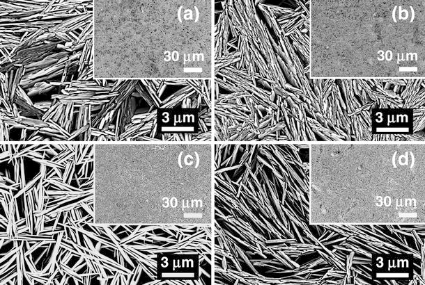
SEM images of ZnO nanowalls electrodeposited with a 0.2 M b 0.175 M c 0.15 M d 0.125 M Zn(NO3)2·6H2O mixed with 0.1 M KCl on ITO–glass at 70°C. Insets show the corresponding low-magnification views illustrating the overall uniformity of the film morphologies
Figure 2.
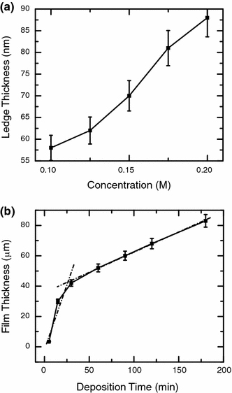
Variations of a mean ledge thickness of nanowalls as a function of initial concentration of Zn(NO3)2·6H2O (mixed with a constant 0.1 M KCl) for a fixed deposition time of 20 min, and b film thickness of nanowalls deposited with 0.1 M Zn(NO3)2·6H2O (mixed with 0.1 M KCl) as a function of deposition time
Figure 3.
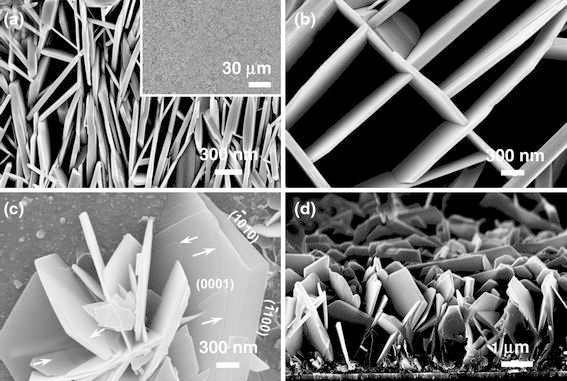
SEM images of nanowalls electrodeposited with 0.1 M Zn(NO3)2·6H2O (mixed with 0.1 M KCl) on ITO–glass at 70°C at different stages of nanowall growth: a, b typical nanowall ledge surface obtained with 60-min deposition time, and c early stage of nanowall formation obtained with 1-min deposition time. d shows a cross-sectional SEM image of the growth of nanowalls directly on ITO–glass obtained with 5-min deposition time
Figure 3 shows more detailed SEM images of nanowalls deposited on ITO–glass in a 0.1 M Zn(NO3)2·6H2O (with 0.1 M KCl) solution at 70°C with different deposition times. Figure 3a shows a magnified SEM image of nanowalls depicting their smooth ledge surfaces, while Fig. 3b illustrates the termination of nanowall growth on the side by the physical obstruction of other nanowalls. It should be noted that the formation of compartment-like structure formed by nanowalls, as shown in Fig. 3b, could occasionally occur on parts of the substrate. Figure 3c shows the early stage of nanowall growth with a deposition time of just 1 min. At the initial stage, ZnO is found to grow as hexagonal disks directly on the ITO surface. Although there appears to be a few nanoparticles on the ITO surface, growth of these particles does not extend over the entire surface prior to the nucleation of nanodisks. Different crystal planes of the hexagonal disks are assigned in Fig. 3c. The assignment of crystal planes is based on the previous reports [3,9] and the TEM investigation of the present work (discussed later). Furthermore, layer-by-layer growth on the (0001) plane (with the new layers marked by arrows) of these hexagonal disks is also evident. With increasing deposition time, the growth on the (0001) plane is eventually stopped by adsorption of Cl− ions (discussed later) and the growth is redirected on the (10 0) and (2
 0) planes, forming nanowalls. The growth evolution of nanowalls with increasing deposition time has been discussed in more details elsewhere [46]. Recently, Yu et al. observed ultraviolet lasing characteristics from ZnO disks synthesized by thermal evaporation at a temperature of 850°C [55]. The present work demonstrates that similar type of hexagonal ZnO disks can also be prepared at a considerably lower deposition temperature and with very short deposition time. Figure 3d shows a cross-sectional SEM view of nanowalls (obtained with 5-min deposition time), confirming the absence of a seeding layer on the ITO surface.
In the lower Zn(NO3)2·6H2O concentration regime (0.001–0.0025 M), no nanowalls are obtained. Figure 4a shows the SEM image of ZnO nanowires deposited on ITO–glass at 70°C for 120 min in a 0.001 M Zn(NO3)2·6H2O (mixed with 0.1 M KCl) solution. ZnO nanowires with an average diameter of 100–120 nm are found to grow uniformly and almost vertically over the entire substrate. A similar type of nanowires with a smaller average diameter (95 nm) is obtained with 0.00075 M Zn(NO3)2·6H2O (SEM image not shown). Figure 4b shows the ZnO nanowires obtained with 0.0005 M Zn(NO3)2·6H2O. These nanowires appear to be less vertically oriented to the substrate, which could be due to the smaller diameter (<50 nm) when compared to that of the thicker nanowires obtained at a higher concentration of 0.001 M. Figure 4c shows the cross-sectional SEM view of nanowire formation on the ITO–glass substrate, depicting the absence of a buffer layer of ZnO on the ITO substrate prior to nanowire formation. The inset of Fig. 4c shows sparsely grown nanowires with a shorter deposition time (30 min), further confirming the direct nanowire growth on the ITO–glass substrate.
Figure 4.
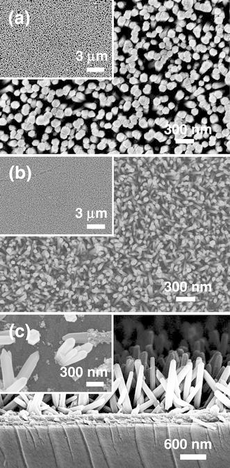
SEM images of nanostructures electrodeposited with a 0.001 M and b 0.0005 M Zn(NO3)2·6H2O (with 0.1 M KCl) on ITO–glass at 70°C for 120-min deposition time. The respective insets show lower-magnification images to illustrate the uniformity. c Shows a representative cross-sectional SEM image of nanowires obtained with 0.001 M Zn(NO3)2·6H2O for 60-min deposition time, and the inset shows sparsely grown nanowires directly on ITO–glass deposited for 30 min
Figure 5 shows the changes in the average diameter and length of the nanowires as functions of electrolyte concentration for a fixed deposition time of 120 min and of deposition time at 0.001 M electrolyte concentration, respectively. The diameter of ZnO nanowires is found to decrease with decreasing Zn(NO3)2·6H2O electrolyte concentration (Fig. 5a), similar to that observed for the mean ledge thickness of nanowalls (Fig. 2a). Recently, Tena-Zaera et al. have succeeded in controlling the diameter of nanowires (from 80 to 300 nm) by increasing the KCl concentration while keeping the ZnCl2 concentration constant [29]. The present result shows that the diameter of ZnO nanowires can be reduced further from 110 to 50 nm with decreasing Zn(NO3)2·6H2O concentration. Our observation (Fig. 5a) is therefore in accord with the previous work by Anthony et al. who also obtained nanowires with smaller diameters with decreasing concentration of zinc electrolyte [28]. The length of nanowires is found to increase almost linearly with increasing deposition time as shown in Fig. 5b[28]. The nanowire growth rates are measured to be 21 nm/min and 13 nm/min during the first 30 min and the next 90 min of deposition, respectively. These growth rates are much smaller than those of nanowalls (1,360 nm/min in the first 30 min of deposition and 288 nm/min in the next 90 min of deposition). The slower growth rates for the nanowires are attributed to the lower initial concentration used for nanowire growth. It should also be noted that these nanowires appear to merge with one another after 120 min of deposition, indicating that the formation of very long nanowires could not be achieved easily by electrodeposition without the use of templates. At a Zn(NO3)2·6H2O concentration lower than 0.0005 M, only a few sparsely grown nanowires but a large number of spherical ZnO nanostructures are obtained. The detail on the formation and characterization on the spherical ZnO nanostructures is published elsewhere [56].
Figure 5.
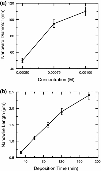
Variations of a average nanowire diameter as a function of initial concentration of Zn(NO3)2·6H2O (mixed with a constant 0.1 M KCl) for a fixed deposition time of 120 min, and b nanowire length deposited with 0.001 M Zn(NO3)2·6H2O (mixed with 0.1 M KCl) as a function of deposition time
The change in the shape and size of ZnO nanostructures can be mainly attributed to the rate of reaction, which depends directly on the initial concentration of the electrolyte used in the electrodeposition. As the current process is a bottom-up approach, a greater number of Zn2+ ions are available at a higher initial concentration, and therefore, a larger number of ZnO nanoparticles can be produced at a faster rate. The self-arrangement of these nanoparticles leads to the formation of different nanostructures, which is directly related to the rate of ZnO nanoparticle formation. In the higher-initial-concentration regime (0.1–0.2 M), we observed the formation of nanowalls with growth occurring in the [10 0] direction, whereas in the lower-concentration regime (0.0005–0.001 M), we obtained nanowires with growth occurring in the [0001] direction (discussed later). At an extremely low electrolyte concentration (0.00025 M), formation of ZnO nanoparticles is expected to be even slower. These nanoparticles are found to self-assemble into spherical hollow nanospheres [56]. In addition to the kinetic effect, other factors such as the nature of the electrolyte also play an important role in generating different nanostructures. The role of Cl− ions in the nanowalls formation is discussed in the next section.
Effect of KCl Concentration on Morphology Control
Although the main objective of using KCl as a supporting electrolyte is to increase the conductivity of the solution used in the electrodeposition of ZnO, KCl can also be used as a capping agent [by adsorption of Cl− ions on the polar (0001) crystal plane of ZnO] to produce 2D nanostructures [45,46]. In a separate set of experiments, we systematically reduced the concentration of KCl while keeping the Zn(NO3)2·6H2O concentration constant, in order to determine the effect of KCl concentration on the morphology of ZnO nanostructures. Figure 6 shows the SEM images of ZnO nanostructures obtained at a constant Zn(NO3)2·6H2O concentration (0.1 M) with different concentrations of KCl. Reducing the KCl concentration from 0.1 M (Fig. 3) to 0.05 M (Fig. 6a) and 0.01 M (Fig. 6b) does not appear to affect the growth of the nanowalls, which suggests that there is a sufficient amount of Cl− ions available for capping the (0001) crystal plane even at a KCl concentration as low as 0.01 M. At a KCl concentration of 0.001 M (Fig. 6c) and in the absence of KCl (Fig. 6d), no nanowall structure is formed. Instead, thicker molehill-like 1D nanostructure is obtained. Unlike the well-defined nanowires obtained with 0.001 M Zn(NO3)2·6H2O (mixed with 0.1 M KCl) as shown in Fig. 4, the molehill-like 1D nanostructures obtained at 0.1 M Zn(NO3)2·6H2O (without and with 0.001 M KCl) are much thicker (with diameter of 400–600 nm) and appear to merge with one another. It should be noted that these molehill-like 1D nanostructures grow as hexagonal grains but lose the distinct hexagonal edge due to side-way growth. In a separate experiment, we repeated the deposition with 0.1 M Zn(NO3)2·6H2O but with a different supporting electrolyte of 0.1 M KNO3. A similar type of thick molehill-like 1D ZnO structures is obtained (SEM not shown). This clearly confirms the important role of the Cl− ions in the formation of 2D ZnO nanostructures, and the Cl− ion concentration can be used to manipulate the growth of 1D nanostructures with larger diameters. Tena-Zaera et al. have systematically studied the role of Cl− ions in the electrodeposition of ZnO nanowire arrays from ZnCl2 solution [29]. They found an increase in the ZnO nanowire diameter with increasing KCl concentration and suggested that the presence of a higher chloride content (>0.1 M) favors lateral growth of nanowires, supporting the earlier studies by Xu et al. on the adsorption of Cl− ions and thus hindering growth on the (0001) plane [45]. The additional experiments presented in the present work further affirm previous hypotheses about the effect of Cl− ions, acting as a capping agent on (0001) plane, and their major role in morphology control for 2D nanowalls and 1D nanostructures with large diameters. It is known that ZnO has both polar (i.e., 0001) and non-polar [(10 0) and (2
 0)] crystal planes. The highly electronegative Cl− ions could easily get attracted to the polar (0001) crystal plane of ZnO. Once a layer of Cl− ions is adsorbed on the (0001) crystal plane, deposition could only occur on the non-polar crystal planes, which causes the individual ZnO hexagonal crystals to grow sideway forming 2D structures. The major difference in the present work when compared to the previous studies is the use of a higher Zn(NO3)2·6H2O electrolyte concentration (0.1 M), which enables the formation of nanowalls by the radial growth occurring along the (10
 0) and (2
 0) planes of ZnO. In contrast, a lower zinc concentration used by Tena-Zaera et al. (0.005–0.0005 M) and Xu et al. (0.05 M) produced thicker nanowires and nanoplatelets, respectively [29,45].
Figure 6.
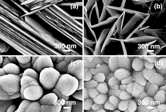
SEM images of ZnO nanostructures obtained from 0.1 M Zn(NO3)2·6H2O mixed with a 0.05 M, b 0.01 M, and c 0.001 M KCl, and d without KCl on ITO–glass at 70°C
Structural Properties
The overall crystal structures of ZnO-nanostructured films are measured by GIXRD and compared with the microstructural characteristics of individual nanowalls and nanowires observed by TEM. Figure 7 shows a representative GIXRD spectrum and TEM images of nanowalls obtained with 0.1 M Zn(NO3)2·6H2O (and 0.1 M KCl). The peak positions of the prominent XRD features for the nanowalls (Fig. 7a) correspond to the wurtzite structure of ZnO (JCPDS 01-076-0704). The most intense diffraction features are found to be from the (101) and (100) planes, indicating the preferential growth directions of nanowalls. The weak features not assigned in Fig. 7a (along with the features observed in the two-theta range of 5–20°—not shown) can be attributed to Zn5(OH)8Cl2·H2O, which is known to form in an electrolyte with Zn2+ concentration higher than 0.01 M [47]. Figure 7b shows a low-magnification TEM image of two nanowall pieces appearing on top of each other (left) and of a few broken smaller pieces (right). The corresponding high-resolution TEM image taken from the thinner section of a plate-like piece is shown in Fig. 7c. A well-resolved lattice with an interlayer spacing of 2.84 Å is observed and found to be in good agreement with the (10 0) plane of ZnO. The corresponding selected-area electron diffraction (SAED) pattern (inset of Fig. 7c) clearly shows the single crystalline nature of individual ZnO nanowalls, which grow along the [10
 0] direction with the top/bottom surface in the (0001)/(000
 ) plane. Similar microstructural properties have been previously reported for nanoplates and nanodisks synthesized by other techniques, including thermal evaporation and solution-based method [3,57]. This confirms that the nanowalls obtained by electrodeposition in the present work (Fig. 7c) belong to the same family of 2D nanostructures as nanoplates or nanodisks.
Figure 7.
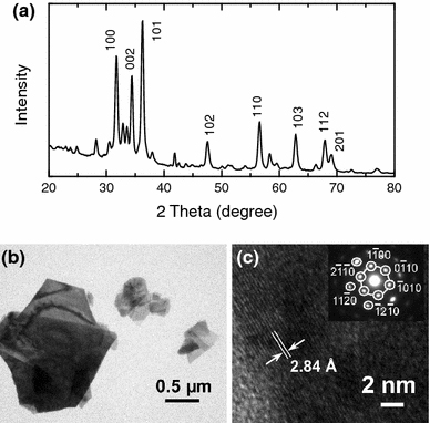
a GIXRD spectra of a nanowall film obtained from 0.1 M Zn(NO3)2·6H2O (with 0.1 M KCl). b Low-magnification TEM image of nanowall pieces and c high-resolution TEM image of a thin section of a nanowall piece. The inset of c shows the corresponding SAED pattern, depicting the single crystalline nature and the growth directions of the nanowalls
Figure 8 shows a typical GIXRD spectrum of the nanowire film and TEM images of an individual nanowire. The GIXRD spectrum over the 2-theta ranges of 20–80° (Fig. 8a) and also of 5–20° (not shown) confirms the wurtzite structure of the ZnO nanowires without any other phases (such as Zn5(OH)8Cl2·H2O found in the nanowall films). In contrast to the nanowall film (Fig. 7a), the (002) line is found to be the singular most intense diffraction feature, indicating the predominant growth direction of ZnO nanowires. The other weaker ZnO XRD features are due to the non-vertically oriented nanowires. Figure 8b shows a TEM image of an individual nanowire, and the lattice spacing as measured from the corresponding high-resolution TEM image (Fig. 8c) is 2.60 Å, indicating that the nanowire grows along the [0001] direction. Furthermore, the corresponding SAED pattern (inset of Fig. 8c) also confirms the growth direction and the single crystalline nature of the ZnO nanowire. The results from the GIXRD and TEM measurements are complementary to each other, and they both firmly establish the different growth orientations of these 2D (Fig. 7) and 1D ZnO nanostructures (Fig. 8).
Figure 8.
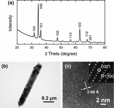
a GIXRD spectra of a nanowire film obtained from 0.001 M Zn(NO3)2·6H2O (with 0.1 M KCl). b Low-magnification TEM image of a nanowire and c high-resolution TEM image of a section of the nanowire. The inset of c shows the corresponding SAED pattern, depicting the single crystalline nature and growth directions of the nanowires
GIXRD measurements were also taken on the samples prepared with a lower concentration and in the absence of KCl. Figure 9 shows the GIXRD spectrum obtained from the sample electrodeposited from 0.1 M Zn(NO3)2·6H2O without KCl at 70°C (Fig. 6d). Unlike the case of nanowalls (obtained with a KCl concentration of 0.01 M or greater), molehill-like ZnO nanostructures formed with 0.001 M KCl or in the absence of KCl exhibit a stronger diffraction intensity from the (002) plane than those of (100) and (101), confirming (002) as the primary growth direction.
Figure 9.
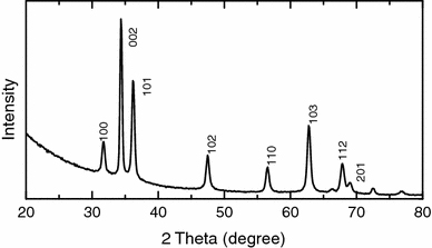
GIXRD spectrum of molehill-like ZnO-nanostructured film obtained from 0.1 M Zn(NO3)2·6H2O without KCl
Conclusions
We have demonstrated a simple electrochemical deposition technique for growing 2D (nanowalls) and 1D (nanowires) ZnO nanostructures on ITO–glass substrates at 70°C in an aqueous Zn(NO3)2·6H2O (mixed with KCl) solution. By judiciously manipulating the deposition conditions, the mean ledge thickness of the nanowalls and the diameter of the nanowires can be controlled over the ranges of 50–100 and 50–120 nm, respectively. The KCl supporting electrolyte concentration can be used to control the morphology of ZnO nanostructures, i.e., 2D and 1D nanostructure growth. The Cl− ions have been found to be an effective capping agent for stopping the growth on the (0001) plane of ZnO and redirecting the growth on the (10 0) plane to produce the nanowalls. In the absence or at a lower concentration (<0.001 M) of KCl, ZnO growth occurs primarily on the (0001) plane, producing molehill-like 1D nanostructures. The crystalline properties and growth direction of the as-synthesized ZnO nanostructures are studied by GIXRD and TEM, which confirm the different growth directions of the nanowalls (10
 0) and nanowires (0001).
Acknowledgment
This work was supported by the Natural Sciences and Engineering Research Council of Canada.
Open Access
This article is distributed under the terms of the Creative Commons Attribution Noncommercial License which permits any noncommercial use, distribution, and reproduction in any medium, provided the original author(s) and source are credited.
References
- Wang ZL. J. 2008. p. 27. COI number [1:CAS:528:DC%2BD1cXnsVamtL0%3D] [DOI] [PubMed]
- Klingshirn C. Phys. Stat. Sol. B. 2007. p. 3027. COI number [1:CAS:528:DC%2BD2sXht1Crs7bE]; Bibcode number [2007PSSBR.244.3027K] [DOI]
- Gao PX, Lao CS, Ding Y, Wang ZL. Adv. 2006. p. 53. and references therein. [DOI]
- Zhang G, Adachi M, Ganjil S, Nakamura A, Temmyo J, Matsui Y. Jpn. J. Appl. Phys. Part 2. 2007. p. L730. COI number [1:CAS:528:DC%2BD2sXhtVelsLbE] [DOI]
- Lorenz M, Kaidashev EM, Rahm A, Nobis Th, Lenzner J, Wagner G, Spemann D, Hochmuth H, Grundmann M. Appl. 2005. p. 143113. Bibcode number [2005ApPhL..86n3113L] [DOI]
- Wang C, Mao B, Wang E, Kang Z, Tian C. Solid State Commun. 2007. p. 620. COI number [1:CAS:528:DC%2BD2sXhvVelsr0%3D]; Bibcode number [2007SSCom.141..620W] [DOI]
- Liu B, Zeng HC. J. 2003. p. 4430. COI number [1:CAS:528:DC%2BD3sXitF2qsr0%3D] [DOI] [PubMed]
- Sun Y, George Ndifor-Angwafor N, Riley DJ, Ashfold MNR. Chem. 2006. p. 352. COI number [1:CAS:528:DC%2BD28XhtF2jsL%2FM]; Bibcode number [2006CPL...431..352S] [DOI]
- Kar S, Dev A, Chaudhuri S. J. Phys. Chem. B. 2006. p. 17848. COI number [1:CAS:528:DC%2BD28Xot12ntr4%3D] [DOI] [PubMed]
- Ayudhya SKN, Tonto P, Mekasuwandumrong O, Pavarajarn V, Praserthdam P. Cryst. 2006. p. 2446. COI number [1:CAS:528:DC%2BD28XhtVSnsbfO] [DOI]
- Santilli CV, Pulcinelli SH, Tokumoto MS, Briois V. J. 2007. p. 3691. COI number [1:CAS:528:DC%2BD2sXnsVSgsL8%3D] [DOI]
- Bhattacharyya P, Basu PK, Saha H, Basu S. Sens. 2007. p. 62. COI number [1:CAS:528:DC%2BD2sXlsF2hs7Y%3D] [DOI]
- Peulon S, Lincot D. Adv. 1996. p. 166. COI number [1:CAS:528:DyaK28Xhs1Wis7c%3D] [DOI]
- Peng W, Qu S, Cong G, Wang Z. Cryst. 2006. p. 1518. COI number [1:CAS:528:DC%2BD28XksFKksbg%3D] [DOI]
- Cao B, Cai W. J. Phys. Chem. C. 2008. p. 680. COI number [1:CAS:528:DC%2BD1cXlslKh] [DOI]
- Gao PX, Ding Y, Wang ZL. Nano Lett. 2003. p. 1315. COI number [1:CAS:528:DC%2BD3sXmsVOnsLY%3D]; Bibcode number [2003NanoL...3.1315G] [DOI]
- Ng HT, Li J, Smith MK, Nguyen P, Cassell A, Han J, Meyyappan M. Science. 2003. p. 1249. COI number [1:CAS:528:DC%2BD3sXlt1Sjsro%3D] [DOI] [PubMed]
- Lao JY, Huang JY, Wang DZ, Ren ZF, Steeves D, Kimball B, Porter W. Appl. Phys. A. 2004. p. 539. COI number [1:CAS:528:DC%2BD2cXlvFaltg%3D%3D]; Bibcode number [2004ApPhA..78..539L] [DOI]
- Lee CJ, Lee TJ, Lyu SC, Zhang Y, Ruh H, Lee HJ. Appl. 2002. p. 3648. COI number [1:CAS:528:DC%2BD38XosVeisrw%3D]; Bibcode number [2002ApPhL..81.3648L] [DOI]
- Jeong JS, Lee JY, Cho JH, Suh HJ, Lee CJ. Chem. 2005. p. 2752. COI number [1:CAS:528:DC%2BD2MXjtlWmsrs%3D] [DOI]
- Shen G, Bando Y, Liu B, Golberg D, Lee CJ. Adv. 2006. p. 410. COI number [1:CAS:528:DC%2BD28Xhs1aksb4%3D] [DOI]
- Li C, Hou K, Lei W, Zhang X, Wang B, Sun XW. Appl. 2007. p. 163502. Bibcode number [2007ApPhL..91p3502L] [DOI]
- Mensah SL, Kayastha VK, Ivanov IN, Geohegan DB, Yap YK. Appl. 2007. p. 113108. Bibcode number [2007ApPhL..90k3108M] [DOI]
- Pradhan AK, Williams TM, Zhang K, Hunter D, Dadson JB, Lord K, Roy UN, Cui Y, Burger A. J. 2006. p. 1985. COI number [1:CAS:528:DC%2BD28XosVegsbw%3D] [DOI] [PubMed]
- Chung TF, Luo LB, He ZB, Leung YH, Shafiq I, Yao ZQ, Lee ST. Appl. 2007. p. 233112. Bibcode number [2007ApPhL..91w3112C] [DOI]
- Fang F, Zhao DX, Zhang JY, Shen DZ, Lu YM, Fan XW, Li BH, Wang XH. Nanotechnology. 2007. p. 235604. Bibcode number [2007Nanot..18w5604F] [DOI]
- Chen Q-P, Xue M-Z, Sheng Q-R, Liu Y-G, Ma Z-F. Electrochem. 2006. p. C58. COI number [1:CAS:528:DC%2BD28XptVCgtA%3D%3D] [DOI]
- Anthony SP, Lee JI, Kim JK. Appl. 2007. p. 103107. Bibcode number [2007ApPhL..90j3107A] [DOI]
- Tena-Zaera R, Elias J, Wang G, Levy-Clement C. J. Phys. Chem. C. 2007. p. 16706. COI number [1:CAS:528:DC%2BD2sXhtFSqsrjF] [DOI]
- Greene LE, Law M, Goldberger J, Kim F, Johnson JC, Zhang Y, Saykally RJ, Yang P. Angew. 2003. p. 3031. COI number [1:CAS:528:DC%2BD3sXlslGksbw%3D] [DOI] [PubMed]
- Gao PX, Song J, Liu J, Wang ZL. Adv. 2007. p. 67. COI number [1:CAS:528:DC%2BD2sXhslGrtLg%3D] [DOI]
- Wang CH, Wong ASW, Ho GW. Langmuir. 2007. p. 11960. COI number [1:CAS:528:DC%2BD2sXhtFKksLfN] [DOI] [PubMed]
- Morin SA, Amos FF, Jin S. J. 2007. p. 13776. COI number [1:CAS:528:DC%2BD2sXhtFyhu73M] [DOI] [PubMed]
- Tong Y, Liu Y, Dong L, Zhao D, Zhang J, Lu Y, Shen D, Fan X. J. Phys. Chem. B. 2006. p. 20263. COI number [1:CAS:528:DC%2BD28Xps1Giuro%3D] [DOI] [PubMed]
- Shen L, Bao N, Yanagisawa K, Gupta A, Domen K, Grimes CA. Cryst. 2007. p. 2742. COI number [1:CAS:528:DC%2BD2sXhtlSgurvJ] [DOI]
- Tian ZR, Voigt JA, Liu J, Mckenzie B, Mcdermott MJ, Rodriguez MA, Konishi H, Xu H. Nature Mater. 2003. p. 821. COI number [1:CAS:528:DC%2BD3sXptlemt74%3D]; Bibcode number [2003NatMa...2..821T] [DOI] [PubMed]
- Izaki M, Omi T. J. 1996. p. L53. COI number [1:CAS:528:DyaK28XitFGgtr0%3D] [DOI]
- Lee S-J, Park SK, Park CR, Lee JY, Park J, Do YR. J. Phys. Chem. C. 2007. p. 11793. COI number [1:CAS:528:DC%2BD2sXnvFOltbs%3D] [DOI]
- Wu Y, Yang B, Zong B, Sun H, Shen Z, Feng Y. J. 2004. p. 469. COI number [1:CAS:528:DC%2BD2cXhtlWmsb4%3D] [DOI]
- Feng X, Li Y, Liu H, Li Y, Cui S, Wang N, Jiang L, Liu X, Yuan M. Nanotechnology. 2007. p. 145706. Bibcode number [2007Nanot..18n5706F] [DOI]
- He W, Gao P, Chu L, Yin L, Li Z, Xie Y. Nanotechnology. 2006. p. 3512. COI number [1:CAS:528:DC%2BD28XhtVaksL3K]; Bibcode number [2006Nanot..17.3512H] [DOI] [PubMed]
- Gautam UK, Vivekchand SRC, Govindaraj A, Rao CNR. Chem. 2005. p. 3995. [DOI] [PubMed]
- Yu T, Zhu Y, Xu X, Shen Z, Chen P, Lim C-T, Thong JT-L, Sow C-H. Adv. 2005. p. 1595. COI number [1:CAS:528:DC%2BD2MXmtlCjtbk%3D] [DOI]
- Yoshida T, Tochimoto M, Schlettwein D, Wohrle D, Sugiura T, Minoura H. Chem. 1999. p. 2657. COI number [1:CAS:528:DyaK1MXmt1Klsro%3D] [DOI]
- Xu L, Guo Y, Liao Q, Zhang J, Xu D. J. Phys. Chem. B. 2005. p. 13519. COI number [1:CAS:528:DC%2BD2MXlsVegsbs%3D] [DOI] [PubMed]
- Pradhan D, Leung KT. J. Phys. Chem. C. 2008. p. 1357. COI number [1:CAS:528:DC%2BD1cXmtF2gsw%3D%3D] [DOI]
- Peulon S, Lincot D. J. 1998. p. 864. COI number [1:CAS:528:DyaK1cXhsFWrtLY%3D] [DOI]
- Cao B, Teng X, Heo SH, Li Y, Cho SO, Li G, Cai W. J. Phys. Chem. C. 2007. p. 2470. COI number [1:CAS:528:DC%2BD2sXot1aluw%3D%3D] [DOI]
- Illy B, Shollock BA, MacManus-Driscoll JL, Ryan MP. Nanotechnology. 2005. p. 320. COI number [1:CAS:528:DC%2BD2MXislCksrs%3D]; Bibcode number [2005Nanot..16..320I] [DOI] [PubMed]
- Gao Y, Nagai M. Langmuir. 2006. p. 3936. COI number [1:CAS:528:DC%2BD28Xit1Okt7s%3D] [DOI] [PubMed]
- Pan H, Feng YP, Lin J, Liu CJ, Wee TS. J. 2007. p. 696. COI number [1:CAS:528:DC%2BD2sXjvVygsro%3D] [DOI] [PubMed]
- Grabowska J, Meaney A, Nanda KK, Mosnier J-P, Henry MO, Duclère J-R, McGlynn E. Phys. Rev. B. 2005. p. 115439. Bibcode number [2005PhRvB..71k5439G] [DOI]
- Kim S-W, Park H-K, Yi M-S, Park N-M, Park J-H, Kim S-H, Maeng S-L, Choi C-J, Moon S-E. Appl. 2007. p. 033107. Bibcode number [2007ApPhL..90c3107K] [DOI]
- Yin Z, Chen N, Dai R, Liu L, Zhang X, Wang X, Wu J, Chai C. J. Cryst. Growth. 2007. p. 296. COI number [1:CAS:528:DC%2BD2sXmt1yltLk%3D]; Bibcode number [2007JCrGr.305..296Y] [DOI]
- Yu D, Chen Y, Li B, Chen X, Zhang M, Zhao F, Ren S. Appl. 2007. p. 091116. Bibcode number [2007ApPhL..91i1116Y] [DOI]
- Pradhan D, Leung KT. J. 2009. p. 4902. COI number [1:CAS:528:DC%2BD1MXotlantrc%3D] [DOI]
- Cao B, Cai W, Li Y, Sun F, Zhang L. Nanotechnology. 2005. p. 1734. COI number [1:CAS:528:DC%2BD2MXhtFChtL7E]; Bibcode number [2005Nanot..16.1734C] [DOI]


