Abstract
The integration ultra-thin high dielectric constant (high-k) materials with graphene nanoribbons (GNRs) for top-gated transistors can push their performance limit for nanoscale electronics. Here we report the assembly of Si/HfO2 core/shell nanowires on top of individual GNRs as the top-gates for GNR field-effect transistors with ultra-thin high-k dielectrics. The Si/HfO2 core/shell nanowires are synthesized by atomic layer deposition of HfO2 shell on highly-doped silicon nanowires with a precise control of the dielectric thickness down to 1–2 nm. Using the core/shell nanowires as the top-gates, high performance GNR transistors have been achieved with transconductance reaching 3.2 mS μm−1, the highest value for GNR transistors reported to date. This method, for the first time, demonstrates the effective integration of ultra-thin high-k dielectrics with graphene with precisely controlled thickness and quality, representing an important step towards high performance graphene electronics.
Graphene, a nearly perfect two-dimensional material, has generated a great deal of interest due to its extraordinary properties and potential applications.1–5 It has been demonstrated that graphene exhibits many unique electronic characteristics, such as ultrahigh carrier mobility exceeding 200,000 cm2V−1s−1,6 a micrometer-scale mean free path, electron-hole symmetry, finite conductivity at zero charge-carrier concentration, and quantum hall effect.7 However, the zero band gap in graphene limits its potential applications in semiconductor technology. Formation of graphene nanostructures, such as nanoribbons or nanomeshes, with the critical dimension below 10 nm can open up an effective conduction band gap8 and enable semiconducting behaviour,9–18 which makes these graphene nanostructures promising candidates for the fabrication of nanoscale transistors.19, 20
To enable high performance graphene or graphene nanoribbon (GNR) transistors requires seamless integration of graphene with high quality high-k dielectric materials. However, deposition of oxide dielectrics on prstine graphene is not straightforward due to the strikingly different chemical nature of these two materials. In particular, it has been proven rather challenging to nucleate and grow a uniform thin layer of high-k dielectrics on graphene using atomic layer deposition (ALD).13, 21–25 To enable effective ALD deposition of oxide dielectrics on graphene requires surface functionalization that either introduces undesired impurities or breaks the chemical bonds in the graphene lattice. These additional processes can often result in a significant degradation in carrier mobilities.26 Introduction of a polymer buffer layer prior to high-k deposition mitigates the potential damage to graphene lattice, 27 but can limit the effective gate coupling due to the low-k polymer layer, and is practically not applicable for the integration of ultra-thin high-k dielectrics with graphene.
We have recently developed a new strategy to integrate high quality dielectric materials with graphene by first synthesizing free-standing oxide dielectric nanostructures at high temperature and then transferring them onto graphene at room temperature. This approach allows graphene-dielectric integration without introducing any appreciable defects into the carbon lattice, and has enabled the highest carrier mobility (>20,000 cm2/Vs) in top-gated graphene transistors.28, 29 In these studies, pure dielectric nanostructures are explored as the top-gate dielectrics for graphene transistors. The dielectric thickness is controlled by the overall dimension of the nanostructures and is difficult to scale down very small thickness (e.g. 1–2nm), due to the difficulties in synthesizing and assembling the oxide nanostructures at such small dimensions. On the other hand, it is of vital importance that one can integrate graphene with ultra-thin dielectric to push the performance of the device.
Here we report a method to fabricate top-gated GNR transistors with ultra-thin high-k dielectrics, by exploiting conductor/dielectric core/shell nanostructures (nanowires or nanoribbons) as the top gate, in which the high-k dielectrics are deposited on conducting (e.g. metal or highly doped semiconductor) nanostructures using ALD with a precise control of the thickness down to 1 nm regime. For example, we have synthesized Si/HfO2 core/shell nanowires by ALD deposition of HfO2 on highly-doped silicon nanowires. Using such core/shell nanowires as the top-gates, we have fabricated GNR transistors with the HfO2 shell as the ultra-thin gate dielectric and the silicon nanowire core as the self-integrated gate electrode. This approach allows effective integration of ultra-thin high quality top-gate dielectrics with graphene, and preserves the integrity of the graphene lattice to afford GNR devices with the highest transconductance of 3.2 mS μm−1 reported to date.
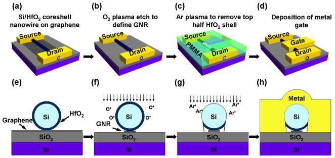
Figure 1 illustrates our approach to fabricate top-gated GNR transistors using a Si/HfO2 core/shell nanowires as the top-gates. The core/shell nanowires were first aligned on top of mechanically peeled graphene flakes on silicon substrate through a physical dry transfer process, followed by an e-beam lithography and metallization process to define the source and drain electrodes (Fig. 1a and e). Oxygen plasma etch was then used to remove the exposed graphene, leaving only the graphene protected underneath the nanowire to form a GNR connected to two big blocks of graphene protected under the source and drain electrodes (Fig. 1b and f). To contact the silicon core gate to external electrode, the top-half of the dielectric shell is etched away using argon plasma (Fig. 1c and g), and the top gate electrode was deposited (Fig. 1d and h). A typical GNR device consists of source, drain and top gate electrodes (Ti/Au, 50 nm/50 nm), Si/HfO2 core/shell nanowire as the top-gate, a highly doped p-type silicon substrate (<0.001 ohm·cm) as the back gate, and a 300 nm thermal silicon oxide layer as the back-gate dielectric.
Fig. 1.
Schematic illustration of the fabrication process to obtain top-gated graphene transistors using Si/HfO2 coreshell nanowires as the etching mask and top-gate. (a) and (e), An Si/HfO2 coreshell nanowire is aligned on top of graphene using a dry-transfer process, and the source-drain electrodes are fabricated by electron-beam lithography. (b) and (f), Oxygen plasma etch is used to remove the unprotected graphene, leaving only the GNR underneath the nanowire connected to two large graphene blocks underneath the source and drain electrodes. (c) and (g), The top-half of the HfO2 shell was etched away using argon plasma to expose the silicon core gate for contact to external electrode. (d) and (h), The top gate electrode is defined through lithography and metallization process.
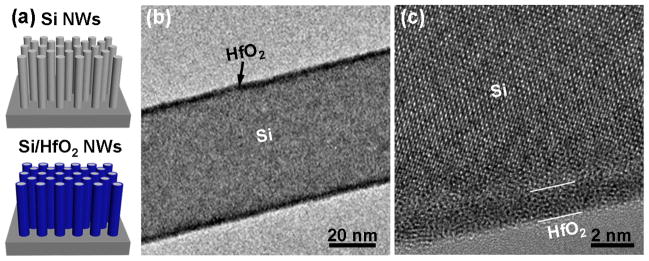
Hafnium oxide has been widely explored in silicon electronics due to its hardness, high chemical stability and excellent dielectric properties, including a high dielectric constant (~ 27), a wide band gap (~ 5.8 eV).30 To grow Si/HfO2 core/shell nanowires, the highly-doped silicon nanowires were first exposed to hydrogen fluoride (HF) vapour to remove the native oxide, and then immediately transferred into ALD chamber to grow HfO2 shell with controlled thickness at 250°C by using tetrakis(dimethylamido) hafnium and water as the precursor and oxidant, respectively (Fig. 2a). The relative dielectric constant is determined to be ~15 based on capacitance-voltage measurement using a planar metal/HfO2/Si control structure, consistent with previous reports on ALD deposited HfO2 film.31 Transmission electron microscope (TEM) image show a uniform coating of the amorphous HfO2 (dark contrast) surrounding the silicon core (light contrast) (Fig. 2b). High resolution TEM image clearly shows the single crystalline silicon core and amorphous HfO2 shell of higher contrast (Fig. 2c). Additionally, there is a thin layer of SiOx transition layer (~0.5 nm) of lower contrast between the silicon core and HfO2 shell, which is also commonly seen in ALD HfO2 film on planar silicon.32–34 The HfO2 film on Si nanowires is generally very smooth with few defects, suggesting that the thickness of HfO2 could be readily controlled with a high degree of uniformity.
Fig. 2.
TEM characterization of Si/HfO2 coreshell nanowires. (a) Schematic illustration of the synthesis of Si/HfO2 coreshell nanowires. Highly doped p-type silicon nanowire arrays were synthesized using catalytic chemical vapour deposition. Atomic layer deposition was used to grow HfO2 shell with controlled thickness. (b) TEM and (c) HRTEM images of Si/HfO2 coreshell nanowires.
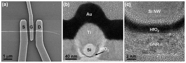
Figure 3a shows a typical top-gated GNR device with Si/HfO2 core/shell nanowire as the top-gate. The gate length is about 500 nm and the diameter of the nanowire is 30 nm. Here the Si/HfO2 core/shell nanowire also functions as a nanoscale etch mask to define a narrow GNR with width in the 10–20 nm regime through aggressive over etch. Cross-section TEM image was used to study the overall gate-stack integration and graphene-HfO2 interface. The complete gate stack (SiO2/graphene/HfO2/Si/Ti/Au) could be readily observed in the low magnification cross-section TEM image (Fig. 3b). A high resolution TEM image of the grapheme-HfO2 interface shows that the graphene layers are intimately integrated with the Si/HfO2 nanowire without any obvious gap or impurities between them (Fig. 3c). A TEM image of multi-layer graphene device is shown here because it is very difficult to visualize the mono- or few-layer of graphene nanoribbon under the nanowire due to significant electron-beam damage while conducting TEM studies. Together, these studies clearly demonstrate that the physical assembly approach can effectively integrate an ultra-thin layer of HfO2 with graphene.
Fig. 3.
Characterization of the graphene/HfO2 interface. (a) A SEM image of a typical device. (b) A cross-section TEM image of the top gate stack. (c) A cross-section HRTEM image of the interface between nanowires and a multi-layers graphene, which indicate that the graphene layers are intimately integrated with the Si/HfO2 nanowire without any obvious gap or impurities between them. A TEM image of multi-layer graphene device is shown here because it is very difficult to visualize the mono- or few-layer of graphene nanoribbon under the nanowire due to significant electron-beam damage while conducting TEM studies.
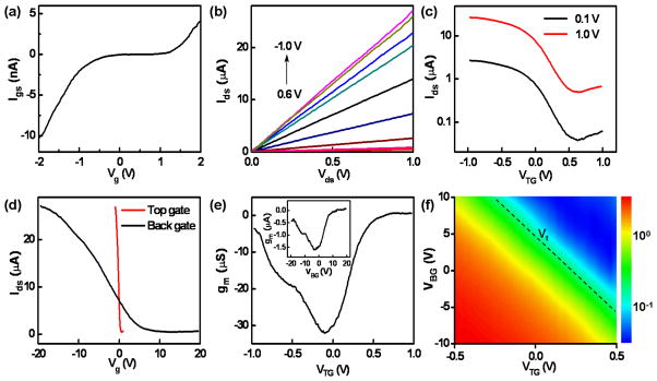
Electrical transport studies of the top-gated device were carried out in ambient condition at room temperature. We have first tested the gate leakage across the Si/HfO2/GNR gate stack before transistor characterization. Importantly, the gate tunnelling leakage current (Igs) from the Si/HfO2 core/shell nanowire to the underlying GNR is negligible within the gate voltage range of ± 1 V range (Fig. 4a). This measurement demonstrates that the 2 nm HfO2 dielectrics can function as an effective gate insulator for top-gated GNR transistors and afford high gate capacitance critical to the high transconductance. The drain-source current (Ids) vs. drain-sourcevoltage (Vds) plots at various top-gate voltages (VTG) show clearly that the device conductance decreases as the gate potential increases towards positive direction (Fig. 4b), demonstrating that the GNR is p-type doped, which can be attributed to edge oxidation or the physisorbed O2 from ambient or during the device fabrication process. Figure 4c shows the transfer characteristics drain-source current (Ids) versus top-gated voltage (VTG) curves for the same device at Vds = 0.1 and 1.0 V. The transfer characteristics show the device can be switched on and off with < 1 volt of gate swing, the smallest on-off gate swing ever achieved in GNR transistors. The device delivers an on-current of 27 μA at Vds = 1 V and Vg = −1.0 V, and shows a room temperature on/off ratio of ~ 70 at Vds = 0.1 V, consistent with a GNR with estimated width of ~10 nm.9–11 To evaluate the top-gated devices versus standard back-gated devices, we have measured the transfer characteristics, Ids-VTG and back-gated voltage (VBG). Significantly, the required gate voltage swing to achieve a similar current modulation in top-gate configuration is more than one order of magnitude smaller dI than that in back-gate configuration (Fig. 4d). The transconductance can be extracted from the Ids-VTG curve. The maximum gm in the top-gated device at Vds = 1V is about 32 μS (Fig. 4e), nearly 19 times of the value obtained in the back-gated configuration (~1.7 μS) (inset, Fig. 4e).
Fig. 4.
Room temperature electrical properties of the top-gated GNR device by using Si/HfO2 coreshell nanowire as the top-gate. (a) Gate leakage current versus top-gate voltage. The leakage current is negligible within ± 1 V range. (b) Ids-Vds output characteristics at variable top-gate voltage starting from 0.6 V at bottom to −1.0 V at top in the step of −0.2 V. (c) The transfer characteristics Ids-VTG at Vds = 0.10 and 1.0 V. (d) Ids-VTG and Ids-VBG transfer characteristics at Vds = 1 V. (e) Transconductance as a function of top-gate voltage VTG and back gate voltage VBG (inset). (f) Two-dimensional plot of the device conductance at varying VBG and VTG bias, the unit in the colour scale is μS.
To further understand the device performance, it is important to determine the gate capacitance, which is not straightforward in our devices due to the complex geometry. To this end, we have employed three-dimensional finite element method to calculate the capacitance of the device, which yields an electrostatic capacitance (Ce) of 3530 nF/cm2 for a 10 nm ribbon under a 30 nm Si/HfO2 core/shell nanowire with 0.5 nm SiOx and 2 nm HfO2 shell. Significantly, these value is already larger than the quantum capacitance (Cq ~ 2000 nF/cm2) in graphene.35 Taking the top-gate capacitance (Ctop) as being the series combination of the electrostatic capacitance (Ce) and the quantum capacitance (Cq), we can obtain Ctop = CqCe/(Ce+Cq) = 1276 nF/cm2. Similarly, we can also calculate the back gate capacitance per area Cback1= 135 nF/cm2 for section without top-gate metal electrode covering, and Cback2 = 11.5 nF/cm2 for the part with top-gate metal electrode covering. The substantial differences are due to the screening effect of the top-gate metal electrode that can significantly decrease (by ~ 1 order of magnitude) the spreading electric field from the back gate. Based on these calculations, a capacitance ratio between the top-gate and the back-gate configuration can be obtained: (CTop·W·L)/(CBack1·W· (L-Ltop)+CBack2·W·Ltop) = ~18.5, where, W is the GNR width, L is the whole channel length, Ltop is width of top-gate metal electrode. To experimentally confirm this capacitance ratio, we have measured the deviceconductance as a function of both VBG and VTG bias (Fig. 4f). This measurements give threshold voltage (Vt) shifts in the top-gate configuration as a function of the applied VBG (Fig. 4f), which can yield the experimental capacitance ratio between top-gate and back-gate configuration, CTG/CBG≈20, consistent with finite element calculation described above. This capacitance ratio is also roughly consistent with the transconductance ratio between the top- and back-gate configurations. Based on these capacitance analyses, we can calculate the hole mobility in the GNR device to be , comparable to the best values reported in GNR transistors.29
It is interesting to compare the top-gated GNR devices with the state-of-the-art silicon MOSFETs. The effective on-current Ion for a transistor is usually characterized at Vds= Vg(on-off) = Vdd, where Vg(on-off) is the gate voltage swing from off- to on-state and Vdd is the power supply voltage. Considering Vds = Vg(on-off) = Vdd = 1V, the Ion of our device at Vds =1V and 1 V gate swing from the off state is ~27μA. Taking the channel width of the GNRs ~ 10 nm, we obtain the scaled values of Ion and gm of our device to be ~2.7 mA μm−1 and ~ 3.2 mS μm−1, exceeding the typical values in sub-100-nm silicon p-MOSFET and n-MOSFET (0.7 mA μm−1 and 0.8 mS μm−1 for p-MOSFET, and 1.66 mA μm−1 and 1.3 mS μm−1 for n-MOSFET) employing high-k dielectrics,36 and is the highest value reported for GNR transistors.29 This is significant because high transconductance is critical to the performance of transistors and voltage gains of transistor-based devices including amplifiers and logic gates.
In conclusion, we have described a rational strategy to integrate pristine graphene with ultra-thin high-k dielectrics, and for the first time demonstrated the fabrication of high performance top-gated GNR transistors with a dielectric thickness as small as 2 nm. This method opens a new avenue to integrate high-k dielectrics on graphene with a precise control of dielectric thickness and quality, and can thus open a new avenue to high performance graphene electronics to impact broadly from high speed circuits to flexible electronics.
References
- 1.Novoselov KS, Geim AK, Morozov SV, Jiang D, Zhang Y, Dubonos SV, Grigorieva IV, Firsov AA. Science. 2004;306:666–669. doi: 10.1126/science.1102896. [DOI] [PubMed] [Google Scholar]
- 2.Bunch JS, Yaish Y, Brink M, Bolotin K, McEuen PL. Nano Lett. 2005;5:287–290. doi: 10.1021/nl048111+. [DOI] [PubMed] [Google Scholar]
- 3.Novoselov KS, Geim AK, Morozov SV, Jiang D, Katsnelson MI, Grigorieva IV, Dubonos SV, Firsov AA. Nature. 2005;438:197–200. doi: 10.1038/nature04233. [DOI] [PubMed] [Google Scholar]
- 4.Zhang YB, Tan YW, Stormer HL, Kim P. Nature. 2005;438:201–204. doi: 10.1038/nature04235. [DOI] [PubMed] [Google Scholar]
- 5.Berger C, Song ZM, Li XB, Wu XS, Brown N, Naud C, Mayou D, Li TB, Hass J, Marchenkov AN, Conrad EH, First PN, de Heer WA. Science. 2006;312:1191–1196. doi: 10.1126/science.1125925. [DOI] [PubMed] [Google Scholar]
- 6.Bolotin KI, Sikes KJ, Jiang Z, Klima M, Fudenberg G, Hone J, Kim P, Stormer HL. Solid State Commun. 2008;146:351–355. [Google Scholar]
- 7.Geim AK, Novoselov KS. Nature Mater. 2007;6:183–191. doi: 10.1038/nmat1849. [DOI] [PubMed] [Google Scholar]
- 8.Son YW, Cohen ML, Louie SG. Phys Rev Lett. 2006;97:216803. doi: 10.1103/PhysRevLett.97.216803. [DOI] [PubMed] [Google Scholar]
- 9.Bai JW, Zhong X, Jiang S, Huang Y, Duan XF. Nature Nanotech. 2010;5:190–194. doi: 10.1038/nnano.2010.8. [DOI] [PMC free article] [PubMed] [Google Scholar]
- 10.Chen ZH, Lin YM, Rooks MJ, Avouris P. Physica E. 2007;40:228–232. [Google Scholar]
- 11.Han MY, Ozyilmaz B, Zhang YB, Kim P. Phys Rev Lett. 2007;98:206805. doi: 10.1103/PhysRevLett.98.206805. [DOI] [PubMed] [Google Scholar]
- 12.Li XL, Wang XR, Zhang L, Lee SW, Dai HJ. Science. 2008;319:1229–1232. doi: 10.1126/science.1150878. [DOI] [PubMed] [Google Scholar]
- 13.Wang HM, Wu YH, Ni ZH, Shen ZX. Appl Phys Lett. 2008;92:053504. [Google Scholar]
- 14.Bai JW, Duan XF, Huang Y. Nano Lett. 2009;9:2083–2087. doi: 10.1021/nl900531n. [DOI] [PubMed] [Google Scholar]
- 15.Jiao LY, Zhang L, Wang XR, Diankov G, Dai HJ. Nature. 2009;458:877–880. doi: 10.1038/nature07919. [DOI] [PubMed] [Google Scholar]
- 16.Kosynkin DV, Higginbotham AL, Sinitskii A, Lomeda JR, Dimiev A, Price BK, Tour JM. Nature. 2009;458:872–U5. doi: 10.1038/nature07872. [DOI] [PubMed] [Google Scholar]
- 17.Ponomarenko LA, Schedin F, Katsnelson MI, Yang R, Hill EW, Novoselov KS, Geim AK. Science. 2008;320:356–358. doi: 10.1126/science.1154663. [DOI] [PubMed] [Google Scholar]
- 18.Liao L, Bai JW, Qu YQ, Huang Y, Duan XF. Nanotech. 2010;21:015705. doi: 10.1088/0957-4484/21/1/015705. [DOI] [PMC free article] [PubMed] [Google Scholar]
- 19.Han MY, Brant JC, Kim P. Phys Rev Lett. 2010;104:056801. doi: 10.1103/PhysRevLett.104.056801. [DOI] [PubMed] [Google Scholar]
- 20.Molitor F, Stampfer C, Guttinger J, Jacobsen A, Ihn T, Ensslin K. Semicond Sci Tech. 2010;25:034002. [Google Scholar]
- 21.Lemme MC, Echtermeyer TJ, Baus M, Kurz H. IEEE Electron Dev Lett. 2007;28:282–284. [Google Scholar]
- 22.Lee BK, Park SY, Kim HC, Cho K, Vogel EM, Kim MJ, Walace RM, Kim JY. Appl Phys Lett. 2008;92:203102. [Google Scholar]
- 23.Wang XR, Tabakman SM, Dai HJ. J Am Chem Soc. 2008;130:8152–8153. doi: 10.1021/ja8023059. [DOI] [PubMed] [Google Scholar]
- 24.Xuan Y, Wu YQ, Shen T, Qi M, Capano MA, Cooper JA, Ye PD. Appl Phys Lett. 2008;92:013101. [Google Scholar]
- 25.Lin YM, Chiu HY, Jenkins KA, Farmer DB, Avouris P, Valdes-Garcia A. IEEE Electron Dev Lett. 2010;31:68–70. [Google Scholar]
- 26.Lin YM, Jenkins KA, Valdes-Garcia A, Small JP, Farmer DB, Avouris P. Nano Lett. 2009;9:422–426. doi: 10.1021/nl803316h. [DOI] [PubMed] [Google Scholar]
- 27.Farmer DB, Chiu HY, Lin YM, Jenkins KA, Xia FN, Avouris P. Nano Lett. 2009;9:4474–4478. doi: 10.1021/nl902788u. [DOI] [PubMed] [Google Scholar]
- 28.Liao L, Bai JW, Qu YQ, Lin YC, Li YJ, Huang Y, Duan XF. Proc Natl Acad Sci USA. 2010 In press. [Google Scholar]
- 29.Liao L, Bai JW, Lin YC, Qu YQ, Huang Y, Duan XF. Adv Mater. 2010 doi: 10.1002/adma.200904415. [DOI] [PMC free article] [PubMed] [Google Scholar]
- 30.Cho MJ, Park J, Park HB, Hwang CS, Jeong J, Hyun KS. Appl Phys Lett. 2002;81:334–336. [Google Scholar]
- 31.Kukli K, Ritala M, Sajavaara T, Keinonen J, Leskela M. Chem Vapor Depos. 2002;8:199–204. [Google Scholar]
- 32.Mitchell DRG, Aidla A, Aarik J. Appl Surf Sci. 2006;253:606–617. [Google Scholar]
- 33.Lu J, Aarik J, Sundqvist J, Kukli K, Harsta A, Carlsson JO. J Cryst Growth. 2005;273:510–514. [Google Scholar]
- 34.Hong JH, Moon TH, Myoung JM. Microelectron Eng. 2004;75:263–268. [Google Scholar]
- 35.Meric I, Han MY, Young AF, Ozyilmaz B, Kim P, Shepard KL. Nature Nanotech. 2008;3:654–659. doi: 10.1038/nnano.2008.268. [DOI] [PubMed] [Google Scholar]
- 36.Chau R, Datta S, Doczy M, Doyle B, Kavalieros J, Metz M. IEEE Electron Dev Lett. 2004;25:408–410. [Google Scholar]


