 One reason for using photonic devices is their
speed—much faster than electronic circuits—but there are many challenges in integrating the
two technologies. Ferrera et al. construct a CMOS-compatible monolithic optical waveform
integrator, a key building block for photonic circuits.
Abstract
All-optical circuits for computing and information processing could overcome the speed limitations intrinsic to electronics. However, in photonics, very few fundamental 'building blocks' equivalent to those used in multi-functional electronic circuits exist. In this study, we report the first all-optical temporal integrator in a monolithic, integrated platform. Our device—a lightwave 'capacitor-like' element based on a passive micro-ring resonator—performs the time integral of the complex field of an arbitrary optical waveform with a time resolution of a few picoseconds, corresponding to a processing speed of ∼200 GHz, and a 'hold' time approaching a nanosecond. This device, compatible with electronic technology (complementary metal-oxide semiconductor), will be one of the building blocks of next-generation ultrafast data-processing technology, enabling optical memories and real-time differential equation computing units.
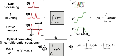
A photonic temporal integrator is a device capable of 'integrating photons', that is, performing the time integral of an arbitrary all-optical input1,2,3,4. Figure 1 (from top to bottom) shows the output time-domain waveforms expected from a photonic integrator for a specific set of input waveforms, chosen to illustrate some of the relevant processing and computing applications of this fundamental device5,6,7, including data processing/analysis8,9, photonic bit counting, optical memory units10,11,12 and analogue computing of differential equations5,13. This last application is particularly interesting: in analogy with its electronic counterpart5, a photonic integrator is the key element to create ultrafast analogue all-optical circuits aimed at solving the differential equations that model fundamental phenomena and applied processes in virtually any field of science or engineering14. As expected for an all-optical technology15,16,17,18,19,20, a photonic integrator can provide a processing speed orders of magnitude faster than its electronic counterpart7. Another striking feature is that it enables the processing of complex information (that is, both amplitude and phase), whereas an electronic integrator is restricted to processing real data7. This feature offers an important additional degree of freedom over an electronic integrator, enabling new applications for advanced information processing and various computing tasks.
Figure 1. Input–output scheme of an optical integrator.
The selected input time-domain waveforms are related with fundamental applications such as: data processing/analysis, bit counting, optical memory units and analogue optical computing of differential equations.
From basic signal processing theory5, it is known that a temporal integrator can be implemented using a linear filtering device with a temporal impulse response (to an input impulse launched at time t=0) of h(t), proportional to the unit step function u(t):
 |
1 |
To realize such a physical system, one must create a structure capable of storing an incoming time-varying optical field and providing an output that is a continuous signal proportional to the total field stored at each instant of time. In electronics, this function can be implemented using a capacitor, which accumulates an electric charge that is proportional to the sum of the incoming electric field. The integrated signal is then proportional to the voltage measured at the capacitor. This principle has no direct analogue in photonics, as, strictly speaking, a complete 'stopping' of photons would be necessary.
The design of a temporal integrator can also be approached by simply considering the device's response in the frequency domain. The spectral transfer function H(ω) of an ideal integrator, calculated as the Fourier transform of the impulse response in equation (1), can be expressed as5
 |
2 |
where 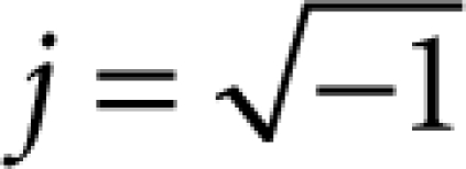 ω is the optical frequency variable and ω0 is the carrier frequency
of the signal to be processed. According to equation (2), an optical integrator should provide
a transmission >1 near ω0 and ideally diverge to infinity at
ω0. Although in principle, this implies the need for gain, it is known
from electronics that the desired response can be 'emulated' within certain limits using
passive filtering architectures7.
A promising general approach for realizing a photonic integrator is based on the use of an optical resonant cavity, for example, a ring resonator or a Fabry–Perot (FP) filter1,13. To simplify the analysis, we consider the case of a general FP cavity composed of two identical mirrors, each characterized by a field reflectivity r (ratio of the reflected and incident field amplitudes, r≤1) and separated by a distance L. Here, the net gain in the cavity medium (round-trip field amplitude gain, excluding mirror loss) is given by a factor γ (γ<1 for loss and γ>1 for gain). In this case, the temporal impulse response is simply given as21
| 3 |
where k=−(1/T)ln(r2γ) and T is the round-trip propagation time in the FP cavity (here, T=2 Ln/c, n being the cavity refractive index and c being the speed of light in vacuum). In simple terms, equation (3) indicates that the signal stored in a FP cavity 'leaks' out with an exponential time decay. Comparing the impulse response of the FP cavity (equation (3)) with that of an ideal integrator (equation (1)), we infer that the FP cavity would behave as a temporal integrator when k=0, that is, r2γ=1. This condition essentially means that, ideally, the cavity should be loss-less. In practice, when k deviates from 0, the device will still perform as a temporal integrator, but only over a limited time window, as determined by the resonator decay time, 1/k. It is also important to note that equation (3) represents the temporal impulse response of a resonant cavity only if the input pulse (1) is spectrally centred at one of the cavity's resonance frequencies, ω0, and (2) it is longer than the round-trip propagation time, T. This translates into an intrinsic limitation in the device processing bandwidth (speed), which is, in effect, constrained by the cavity's free spectral range (FSR=1/T).
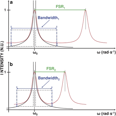
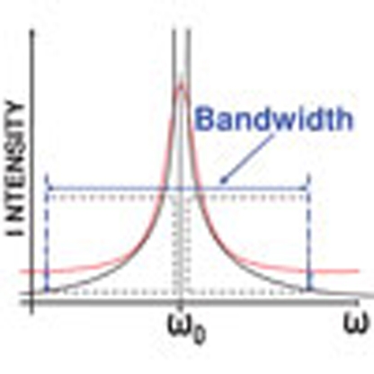
This principle can be better illustrated by evaluating the frequency response of a general optical resonant cavity21. The spectral transfer function of a standard optical resonator, such as the FP, is a periodic frequency comb with a period fixed by the FSR, in which the shape of the spectral response around any given resonance is well approximated by a Lorentzian function. Figure 2 illustrates the matching between the amplitude spectral transfer functions of an ideal integrator (black curve, defined by equation (2)) and an optical resonator (red curves) around a specific resonance ω0. For comparison, we show two different resonators (case a and b, respectively) that differ only in their FSRs. In each case, the regions inside the dashed boxes represent the frequency range over which the resonator response resembles very nearly that of an ideal integrator. From this representation, it can be easily understood how a larger FSR (that is, a shorter round-trip propagation time achieved through a reduction of the physical device dimensions) translates into a broader integration bandwidth, that is, a higher processing speed.
Figure 2. Operational limits of an optical resonator used as an integrator.
The picture shows the typical fit between the spectral intensity transfer functions of a general resonator (Lorentzian curve in red) and that of an ideal integrator (black curve). The plot makes a comparison in terms of integration bandwidth between two resonators (case a, b) with two different FSRs. A longer FRS (FSR1>FSR2) corresponds to a broader integration bandwidth (bandwidth1>bandwidth2).
In this paper, we report the first implementation of a monolithic all-optical temporal integrator. The complementary metal-oxide semiconductor (CMOS)-compatible micro-ring resonator that we used in our experiment is a fully passive device, despite the fact that gain has been thought to be necessary1,13 to achieve the stringent specifications that are required for time integration2. Previous, non-integrated passive optical integrators suffered from very limited, impractical, operational time windows of <50 ps22. Although adding gain1,13 could improve this, it would also come at the expense of limiting processing speeds to <20 GHz13, while adversely affecting noise characteristics. Using our entirely passive device, we show accurate temporal integration of arbitrary complex-field optical waveforms with time features as short as ∼8 ps, about an order of magnitude faster than the best results achieved with active photonic integrators13, and over an integration time window of ∼800 ps, more than an order of magnitude longer than previous passive photonic integrators22. This time resolution corresponds to a remarkable processing speed as high as ∼200 GHz. Thus, this device offers a processing time-bandwidth product (TBP, a principal figure of merit, defined as the ratio between the integration time window to the fastest time feature that can be accurately processed) approaching 100, much higher than advanced passive electronic integrators (TBP <10)7 and even significantly larger than previously shown active photonic integrators (TBP <30)13.
Results
Device structure
The device reported here is based on a passive integrated four-port high-index contrast glass micro-ring resonator with a FSR of 200 GHz and a Q factor of ∼1.2 million23. Doped silica glass films were deposited using standard chemical vapour deposition, and waveguides were patterned using photolithography and reactive ion etching. The entire fabrication process is CMOS compatible24,25,26,27, with no further requirement for high-temperature post-processing. Propagation losses are very low, at less than 6 dB m−1, whereas the total fibre to fibre insertion loss is ≅9 dB, owing to additional coupling losses from the bus waveguide to the ring and vice versa.
Experiment overview
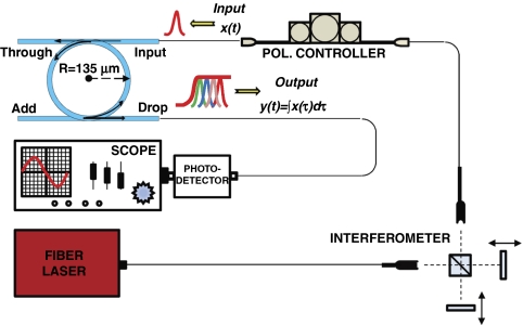
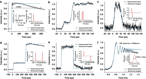
Figure 3 shows the experimental setup, as well as the working principle of our optical integrator. The laser source emits Gaussian pulses, each with a time duration of ∼7.5 ps (see Methods for definitions) at a repetition rate of 16.9 MHz. By means of an interferometer-based optical pulse shaper, we generated three different input waveforms: (1) an ultrashort optical pulse directly generated by the laser source (see inset (B) in Fig. 4a), (2) a sequence of two consecutive, in-phase pulses (see insets in Fig. 4b,d) and (3) a sequence of two consecutive, π-phase-shifted pulses (see insets in Fig. 4c,e). The temporal distance between the pulses was either set at 40 or 275 ps for both inputs (2) and (3). The signal was then launched into the input port of the ring, while the output waveform at the drop port was directed to a high-speed photo-detector (∼12 ps response time) in conjunction with a 50-GHz sampling oscilloscope. The normalized intensity profiles of the time-domain waveforms at the device output are shown (main plots—solid black curves) in Figure 4a for single input pulses (1) and in Figure 4b–e for the double input pulses (2) and (3). The corresponding theoretical cumulative integrals of the ideal input waveforms are represented by the solid blue curves in the main plots of Figure 4.
Figure 3. Experimental setup.
The image reports the physical dimensions of the ring, the working principle as an optical integrator and a detailed scheme of the experimental setup used during the measurements. First, the optical pulse train is emitted (on a frequency carrier that is in resonance with the ring) by a picosecond fibre laser and is then reshaped into one of the waveforms under investigation by the interferometer. Subsequently, the desired signal passes through a controller that fixes its polarization before being launched inside the cavity. Finally, the optical ring output is recorded (in the time domain) by means of a high-speed photo-detector connected to a sampling oscilloscope.
Figure 4. Analysis of the integrator's temporal response.
The main plots represent both the experimental (black curve) and the theoretical (blue curve) time integrals (intensity waveforms) of all the optical input waveforms under analysis. The latter are reported in the corresponding insets (red curves). The measurement is performed for different cases: an ultrashort optical pulse directly generated by the laser source (a); in-phase pulses with a relative temporal delay of 40 ps (b); π-shifted pulses with a relative temporal delay of 40 ps (c); in-phase pulses with a relative temporal delay of 275 ps (d); π-shifted pulses with a relative temporal delay of 275 ps (e); a linearly chirped (quadratic phase) broadband optical pulse, with a field amplitude FWHM time duration of ∼1,340 ps (f). The impulse response (a, inset (A)) was obtained by using a fast (τ∼8 ps) amplified photo-detector. The dispersed pulse was calculated by assuming an ideal quadratic phase variation on the measured temporal amplitude pulse profile according to the linear dispersion value (∼2,000 ps nm−1) of the fibre-dispersive element used in our experiments.
Single-pulsed experiments
The output waveform in Figure 4a closely approximates the temporal impulse response of the device, as the bandwidths of the input pulse and the integrator are close to each other. From the measured temporal impulse response, which closely follows the theoretical curve defined by equation (3), we estimate an integration time window (defined as the decay time required to reach 80% of the maximum intensity) of ∼800 ps. The device response to an ultrashort input pulse (1), recorded using a faster photo-detector (∼8 ps rise time), is represented in the inset (A) of Figure 4a, in which a rise time of ∼8 ps (10–90%) is estimated. In experiments with devices having smaller ring radii (47.5 μm), we achieved much higher processing speeds (up to ∼500 GHz) and a higher throughput (from ∼0.015% for the device reported here to ∼1.5%), although this comes at the expense of a shorter integration time window.
Double-pulsed experiments
The results for the double-pulsed experiments show that the integrator simply sums up the area under the two field amplitude waveforms for the case with no phase difference (Fig. 4b,d). In contrast, when the pulses are out of phase, the time integral of the second optical pulse compensates that of the first pulse (assuming the two pulses are nearly identical), leading to a square-like time profile with a duration given by the input inter-pulse delay (Fig. 4c,e). These results suggest a number of important applications for the proposed photonic integrator, such as a 1-bit optical memory unit, which can be loaded, that is, switched to the state '1', by launching an input 'set' pulse, and subsequently erased, or reset, to the state '0' by a pulse π-phase shifted with respect to the 'set' pulse12. In this scheme, the memory switching time is fixed by the integrator processing speed and the memory lifetime is determined by the integration time window (∼8 and ∼800 ps, respectively, as previously mentioned). We recall that all of the plots in Figure 4 are expressed in terms of intensity, as this is normally relevant for optical processing and measurement. Therefore, considering that (as discussed above) the device integrates the field amplitude of the pulses coherently, Figure 4b,d shows an ∼1:4 increase for the in-phase two-pulse integration experiments, whereas a measurement of the output field amplitude would yield a step ratio of 1:2.
Complex integration
The results shown in Figure 4 confirm that this integrator operates on the complex temporal field envelope (amplitude and phase) of the optical signals. To highlight this, we performed the temporal integration of a complex optical waveform having a large TBP (>100). In this case, the input optical pulses (see inset in Fig. 4f) were obtained by dispersing the broadband laser pulses in time by linear propagation through a fibre-dispersive element, to produce strong linearly chirped pulses with an intensity FWHM time duration of ∼950 ps (field FWHM time duration of ∼1,340 ps). The chirped pulses were then launched into the ring resonator and the temporal intensity waveform was measured at the output (drop port) of the resonator. Figure 4f shows the experimental results (black curve) together with the theoretical time integral (blue curve) of the chirped optical pulse. Despite the high complexity of the output waveform, the experimental and theoretical curves agree well over timescales longer than the resolution of the device (∼8 ps). This last result suggests that it should be possible to recover the temporal phase information of a given arbitrary optical waveform from the temporal intensity profile at the output of our device, similar to a recent phase recovery method developed using an optical differentiator28.
Discussion
As for any passive photonic time integrator2,3,4, the overall energetic efficiency of our device is fundamentally limited by the ratio of the resonator line width to the signal spectral bandwidth. In our case, the resonator line width of ∼400 MHz and signal spectral bandwidth of ∼110 GHz (both values are defined as the full width at 10% of the maximum transmission. The FWMH of the resonator is 160MHz.) yield a maximum theoretical efficiency of approximately −24 dB. In practice, the effective throughput will be reduced by coupling losses or any non-ideal energy transfer of the cavity at the resonance frequency. Introducing gain, for example, through four-wave mixing23,24,29,30, would potentially improve the energetic efficiency, as well as the quality of the response function.
As illustrated in Fig. 2, the response of a passive resonator deviates from the ideal one, particularly in the spectral region near the resonance frequency, ω0. In fact, the shape of the spectral response around any given resonance is well approximated by a Lorentzian function, which is indeed the spectral transfer function corresponding to the temporal impulse response in equation (3), H(ω)∝[j(ω−ω0+k)]−1. Thus, the approach of introducing gain into the cavity (by increasing γ) has been proposed1,13 in order to better approximate an ideal integrator, that is, k=0, given (as stated above) by r2γ=1, which dictates an exact balance of loss and gain in the resonant cavity. However, we recall that an active integrator also has significant drawbacks13 such as a high noise level (originating from spontaneous emission), high energy consumption and additional technical challenges for fabrication and operation of the device, particularly for integrated solutions. Furthermore, achieving gain may require increasing the device size, which would lead to a reduced processing bandwidth. As already mentioned, active photonic integrators, demonstrated using resonant cavities based on optimized fibre Bragg gratings13, have relatively limited processing speeds (<20 GHz), although still higher than the most advanced electronic technologies7. Although these drawbacks could be overcome using passive optical filters2,3,4, these suffer from a poor throughput (the input–output energetic efficiency) and a limited integration time window22. It has been estimated2 that in order to achieve near ideal integrator performance using a passive resonant cavity, the field reflectivity of each mirror should be r>99.99%, assuming no additional propagation losses (γ=1), yielding a total round-trip loss of less than ∼10−4, an immensely challenging requirement. The photonic integrator reported here, based on a high-Q micro-resonator, is capable of meeting these stringent requirements.
In summary, this work reports the first monolithic all-optical temporal integrator. The device, based on a passive high-Q micro-ring resonator, allows us to achieve temporal integration of complex-field optical waveforms, with a resolution of ∼8 ps, well beyond the reach of electronics, and with a 'hold' time window as long as a nanosecond. The achievement of this in a CMOS-compatible photonic chip offers significant promise for fully integrated ultrafast optical information processing, memory, measurement and computing systems.
Methods
Waveform generation
We used a passively mode-locked fibre laser (PriTel) to generate transform-limited Gaussian-like optical pulses with a pulsewidth of ∼7.5 ps (defined as the half width at1/e (HW1/e) of the field amplitude, which corresponds to a full width at half maximum (FWHM) of the pulse intensity of ∼8.8 ps, as determined by spectral interferometry), at a repetition rate of 16.9MHz. The laser light beam was first sent to an optical pulse shaper (Michelson interferometer, see Fig. 3), which was used to generate the three different kinds of input waveforms reported in the insets of Figure 4a–e. By coarsely varying the optical path difference of the interferometer, the temporal distance between the pulses was set at 40 and 275 ps for both the in-phase and π-phase-shifted pulses. The phase shift between pulses was precisely set by a piezo controller mounted on one of the two mirrors of the pulse shaper. The phase-shift value was confirmed through a measurement of the optical spectrum of the two interfering pulses (for example, a π (zero)-phase shift between the two delayed pulses translates into a zero (peak) in the spectral interference pattern at the pulses' central frequency). The pulses were then sent through a polarization controller to produce a TE polarization, while the central wavelength was tuned to the transverse electric (TE) resonance at 1559.46 nm.
The fibre-dispersive element, used to obtain the optical pulse represented in the inset of Figure 4f, was a 10 m long, linearly chirped fibre Bragg grating operated in reflection (incorporated in an optical circulator), which introduced a group velocity dispersion of 2,000 ps nm−1 over the entire bandwidth of the input laser pulses. This optical device allowed us to induce a strong dispersion on the input broadband pulses with negligible nonlinear effects.
Optical detection
The temporal intensity profiles of the signals at the ring integrator output were measured using a high-speed photo-detector (∼12 ps response time) connected to a sampling oscilloscope (Tektronix CSA8200, real-time bandwidth=50 GHz). To characterize the device response to ultrashort input pulses (that is, the time impulse response), we used, in conjunction with the sampling oscilloscope, a photo-detector with a faster response time of ∼8 ps. The result (Fig. 4a, inset (A)) shows a rise time of ∼8 ps (10–90% of the maximum output), which was still limited by the photo-detector response time. The ripple observed in the 'flat-top' of the impulse response is partly due to the impulse response of the photo-detector.
Author contributions
J.A., D.J.M. and R.M. provided management oversight for this project. M.F., Y.P. and L.R. carried out the measurements and analyzed the data. S.T.C. and B.E.L. designed and fabricated the devices. All the authors contributed to design the experiments and to prepare the final paper.
Additional information
How to cite this article: Ferrera, M. et al. On-chip CMOS-compatible all-optical integrator. Nat. Commun. 1:29 doi: 10.1038/ncomms1028 (2010).
Acknowledgments
This work was supported by the Australian Research Council (ARC) Centres of Excellence program, the FQRNT (Le Fonds Québécois de la Recherche sur la Nature et les Technologies), the Natural Sciences and Engineering Research Council of Canada (NSERC), the NSERC Strategic Projects and the INRS. L.R. wishes to acknowledge a Marie Curie Outgoing International Fellowship (contract no. 040514).
References
- Ngo N. Q. Optical integrator for optical dark-soliton detection and pulse shaping. Appl. Opt. 45 6785–6791 (2006). [DOI] [PubMed] [Google Scholar]
- Ngo N. Q. Design of an optical temporal integrator based on a phase-shifted Bragg grating in transmission. Opt. Lett. 32 3020–3022 (2007). [DOI] [PubMed] [Google Scholar]
- Azaña J. Proposal of a uniform fiber Bragg grating as an ultrafast all-optical integrator. Opt. Lett. 33 4–6 (2008). [DOI] [PubMed] [Google Scholar]
- Preciado M. A. & Muriel M. A. Ultrafast all-optical integrator based on a fiber Bragg grating: proposal and design. Opt. Lett. 33 1348–1350 (2008). [DOI] [PubMed] [Google Scholar]
- Oppenheim A. V., Willsky A. S. & Nawab S.H. Signals and Systems, 2nd edn (Prentice Hall, 1996). [Google Scholar]
- Hsue C. -W., Tsai L. -C. & Chen K. -L. Implementation of first-order and second-order microwave differentiator. IEEE Trans. Microw. Theory Tech. 52 1443–1448 (2004). [Google Scholar]
- Hsue C. -W., Tsai L. -C. & Tsai Y. -H. Time-constant control of microwave integrators using transmission lines. IEEE Trans. Microw. Theory Tech. 54 1043–1047 (2006). [Google Scholar]
- Miller D. A. B. Are optical transistors the logical next step? Nat. Photonics 4 3–5 (2010). [Google Scholar]
- Cotter D. et al. Nonlinear optics for high-speed digital information processing. Science 286 1523–1528 (1999). [DOI] [PubMed] [Google Scholar]
- Hill M. T. et al. A fast low-power optical memory based on coupled micro-ring lasers. Nature 432 206–209 (2004). [DOI] [PubMed] [Google Scholar]
- Ding Y., Zhang X., Zhang X. & Huang D. Active microring optical integrator associated with electroabsorption modulators for high speed low light power loadable and erasable optical memory unit. Opt. Express 17 12835–12848 (2009). [DOI] [PubMed] [Google Scholar]
- Asghari M. H., Park Y. & Azaña J. Demonstration of a photonic integrator-based loadable and erasable optical memory unit with picosecond switching time. 35th European Conference on Optical Communication ECOC, Proceeding P1.18 (2009). [Google Scholar]
- Slavík R. et al. Photonic temporal integrator for all-optical computing. Opt. Express 16 18202–18214 (2008). [DOI] [PubMed] [Google Scholar]
- Simmons G. F. Differential Equations with Applications and Historical Notes 2nd edn (McGraw-Hill, 1991). [Google Scholar]
- Venema L. Photonic technologies. Nature 424 809 (2003). [Google Scholar]
- Foster M. A. et al. Silicon-chip-based ultrafast optical oscilloscope. Nature 456 81–84 (2008). [DOI] [PubMed] [Google Scholar]
- Azaña J., Madsen C. K., Takiguchi K. & Cincontti G. Optical signal processing. IEEE/OSA J. Lightwave Technol. 24 2484–2767 (2006). [Google Scholar]
- Vasilyev M., Su Y. & McKinstrie C. Nonlinear-optical signal processing. IEEE J. Sel. Top. Quantum Electron. 14 527–971 (2008). [Google Scholar]
- Madsen C. K., Dragoman D. & Azaña J. Signal analysis tools for optical signal processing. EURASIP J. Appl. Signal Processing 2005 1449–1623 (2005). [Google Scholar]
- Miller A. Optical computing: elements of an optical engine. Nature 323 13–14 (1986). [Google Scholar]
- Madsen C. K. & Zhao J. H. Optical Filter Design and Analysis: A Signal Processing Approach (John Wiley & Sons, 1999). [Google Scholar]
- Park Y., Ahn T. -J., Dai Y., Yao J. & Azaña J. All-optical temporal integration of ultrafast pulse waveforms. Opt. Express 16 17817–17825 (2008). [DOI] [PubMed] [Google Scholar]
- Ferrera M. et al. Low power four wave mixing in an integrated, micro-ring resonator with Q=1.2 million. Opt. Express 17 14098–14103 (2009). [DOI] [PubMed] [Google Scholar]
- Ferrera M. et al. Low-power continuous-wave nonlinear optics in doped silica glass integrated waveguide structures. Nat. Photonics 2 737–740 (2008). [Google Scholar]
- Miller D. A. B. Optical interconnects to silicon. IEEE J. Sel. Top. Quantum Electron. 6 1312–1317 (2000). [Google Scholar]
- Izhaky N. et al. Development of CMOS-compatible integrated silicon photonics devices. IEEE J. Sel. Top. Quantum Electron. 12 1688–1698 (2006). [Google Scholar]
- Gondarenko A., Levy J. S. & Lipson M. High confinement micro-scale silicon nitride high Q ring resonator. Opt. Express 17 11366–11370 (2009). [DOI] [PubMed] [Google Scholar]
- Li F., Park Y. & Azaña J. Complete temporal pulse characterization based on phase reconstruction using optical ultrafast differentiation (PROUD). Opt. Lett. 32 3364–3366 (2007). [DOI] [PubMed] [Google Scholar]
- Levy J. S. et al. CMOS-compatible multiple-wavelength oscillator for on-chip optical interconnects. Nat. Photonics 4 37–40 (2010). [Google Scholar]
- Razzari L. et al. CMOS-compatible integrated optical hyper-parametric oscillator. Nat. Photonics 4 41–45 (2010). [Google Scholar]


