Abstract
Due to their toxicity to humans and animals, heavy metals and nitrate in groundwater are of particular concern. The combination of high toxicity and widespread occurrence has created a pressing need for effective monitoring and measurement of nitrate and heavy metals in soil pore water and groundwater at shallow depths. In this work, a new electrochemical sensing platform with the self-assembly nanobeads packed (nBP) hetero columns has been developed for the pH and nitrate measurements. In addition, for on-site determination of cadmium (Cd(II)), a bismuth (Bi(III)) based polymer lab chip sensor using the square-wave anodic stripping voltammetry (SWASV) sensing principle has been designed, fabricated and successfully characterized. Factors affecting sensitivity and precision of the sensor, including deposition potential and deposition time, were studied. Miniaturized electrochemical lab chip sensors could be very valuable in environmental monitoring area due to their many benefits, such as greatly reduced sensing cost, sensing system portability, and ease of use.
Keywords: Bismuth, Cadmium, Nitrate, Polymer lab chip sensor, Square-wave anodic stripping voltammetry (SWASV)
1. Introduction
As a viable alternative for potable water production, the groundwater is preferably considered because under most conditions it tends to be cleaner and safer than surface waters contaminated directly by waste products or other substances which changes the water properties. So, the cold groundwater filtered through the ground can provide drinking water of acceptable quality with minimal treatment and at modest cost. It has been estimated that about 48% of the total population and 95% of the rural population of the United States are relied upon groundwater for water supply [1]. However, due to excessive dependence on groundwater, both for irrigation and drinking water coupled with over exploitation of ground water, there has been an apparent tendency for the quality of groundwater to deteriorate, which has been caused by various toxic substances [2, 3]. Nitrate (NO3 −-N) and heavy metals contamination and the associated health concerns are among the most common problems adversely affecting groundwater quality in the United States and throughout the world [4-7]. Toxicity of nitrate and heavy metals to human being and other living organisms has been studied extensively and has been implicated as a cause of a variety of diseases [8]. In this work, cadmium (Cd(II)) was considered to be the pollutant, which is often typical of cases in which groundwater is contaminated from the release of a single heavy metal [9]. Cadmium adversely affects several important enzymes and is known to accumulate in the human kidney for a relatively long time, and at high dose, it is also known to produce health effects on the respiratory system [10]. In addition, the elevated levels of nitrate in drinking water are related primarily to human health effects such as methemoglobinemia (infantile cyanosis), neural tube effects, or spontaneous abortions [11]. Recently, epidemiological studies have suggested that high nitrate ingestion may also be a contributing factor in gastric cancer [8].
Typically, environmental sampling methods for these contaminants are accomplished by invasively collecting samples in the field and transporting them to centralized laboratories for analyses. Unfortunately, since their speciation can often be changed quickly as a result of chemical, biological and physical reactions, the time delays associated with this procedure are frequently unacceptable. Furthermore, these sampling methods can be very costly and time consuming [12]. Thus, it is desirable to prevent the sample alterations associated with the transport delays by performing analyses rapidly and on-site, which is a crucial issue in environmental monitoring. A significant advantage of micro electro mechanical system (MEMS) is the ability to make possible mechanical parts of micron size that can use very small volumes (a few μL). In addition, the mass production ability of MEMS technology, due to its batch fabrication methods, permits use of low cost components with high accuracy and reliability, which are vital for effective sample mixing, separation, etc. The use of lab chip concept enables miniaturized instruments for detecting nitrate, pH and heavy metals in the surface waters and groundwater at shallow depths.
In this work, a new self-assembly nanobeads packed (nBP) hetero column on a polymer lab chip was developed for potentiometric pH and nitrate measurements. When making planar ion-selective microelectrode and Ag/AgCl reference microelectrode with using MEMS fabrication technologies, the main problems are how to hold liquid ion exchange (LIX) membrane to permit ions selectivity and how to contain the internal KCl solution to make a reliable liquid-liquid junction Ag/AgCl reference microelectrode. In order to solve these problems, the hydrophilic or hydrophobic nanobeads were partially packed in a designated region by capillary electrophoresis. In addition, a polymer lab chip integrated with electrochemical sensors using the square-wave anodic stripping voltammetry (SWASV) procedure was developed to measure the concentration of Cd(II) in aqueous samples. Generally, mercury-based stripping voltammetric techniques are well known as powerful techniques for multi-element trace heavy metal determinations in environmental, biological and industrial samples [13]. Despite their remarkable sensitivity, however, there is a need to replace the toxic mercury with more environmentally friendly materials [14]. As an alternative to mercury, bismuth, known as a “green metal”, has recently been used as the working electrode in connection with these stripping techniques. Accordingly, the major objective of this study was to develop and characterize an ion-selective pH and nitrate chip sensor and a heavy metal chip sensor by using microfabrication technology that can lead to a portable instrument.
2. Materials and methods
2.1. Materials
Materials were purchased as follows: The aqueous colloidal silica solution from Bang’s Laboratories Inc. (800nm, Fisher, IN, USA); surfactant-free polystyrene (PS) solution from Polysciences, Inc. (800nm, Warrington, PA, USA); hydrogen ionophore I - cocktail B and nitrate ionophore - cocktail A from Sigma-Aldrich (Allentown, PA, USA); bismuth rods (99.99%) from ESPI Metals (Ashland, OR, USA) used as the metal source for the e-beam evaporator (Temescal FC1800, BOC Edwards Temescal, Livermore, CA, USA) to fabricate the planar Bi microelectrodes; the buffer solution was made by mixing acetate buffer (Sigma-Aldrich Corp., MO, USA) and 0.1 M KCl (Sigma-Aldrich Corp., MO, USA) in deionized (DI) water at pH 4.65. All chemicals were used as received. All experiments were carried out at room temperature to eliminate any temperature effects.
2.2. Ion-selective chip sensor
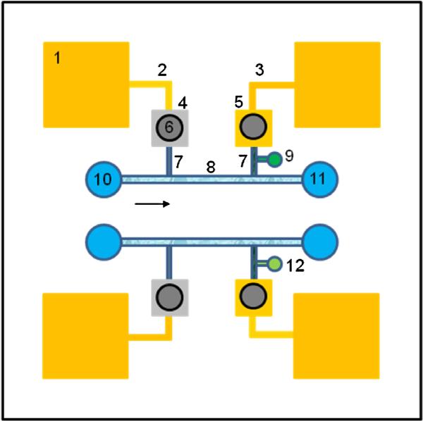
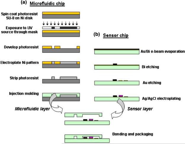
For making the potentiometric lab chip sensor, as shown in Figure 1, a microfluidic chip and a microsensor chip with planar microelectrodes was fabricated and then bonded by the fusion bonding method. For a microfluidic chip, a cyclic olefin copolymer (COC, Topas 5013, Ticona, Summit, NJ, USA) plastic chip patterned with microfluidic channels was prepared by an injection molding technique using an electroplated nickel mold [15]. More specifically, SU-8 2075 photoresist (Microchem Corp., Newton, MA, USA) was spin-coated on a 3-inch diameter nickel (Ni) disk to achieve a 100 μm thickness, followed by a pre-bake process. After the photoresist layer was exposed to a UV source (365 nm UV), it was baked again for cross-linking for about five hour. After developing, Ni electroplating was performed in a Ni plating bath, using a two-electrode system with a Ni anode and the patterned Ni disk cathode. Finally, a Ni mold with a 100 μm-thick plating Ni microstructure was obtained after removal of the residual SU-8. The microfluidic chip was then replicated from this mold in a COC substrate by a high-throughput injection molding machine (BOY 22A, BOY Machines Inc., Exton, PA, USA).
Fig. 1.
Conceptual illustration of self-assembly nBP hetro columns on a lab chip for the dual pH and nitrate measurements (1. Contact pad; 2. Reference electrode; 3. Working electrode; 4. Ag; 5. Au; 6. 3M KCl solution; 7. Self-assembly PS nBP column; 8. Self-assembly silica nBP column; 9. pH ionophore solution; 10. Influent; 11. Effluent; 12. Nitrate ionophore)
In order to hold the LIX membrane and to contain the internal KCl solution, nanobeads packing technique was applied to the predetermined microfluidic channel. For a Ag/AgCl reference microelectrode, the patterned COC chip substrate was pretreated with O2 plasma for 2 min to give high hydrophilicity to the microchannel surface [15]. The aqueous colloidal silica solution was heated to 65 °C in a beaker with gentle stirring (80 rpm) to prevent slow precipitation of the aggregated silica particles. Pretreated open microchannels allowed the aqueous colloidal silica solution to drive to the end of the channels by capillary action. Once the colloidal silica particles reached the end of a microchannel, spontaneous three-dimensional packing of the silica beads started from the end of the microchannel due to the slow evaporation of solvent. Subsequently, the self-assembled nanobead packing process continued toward the end of the empty microchannel at the bottom. For an ion-selective membrane, plasma-treated open microchannel was dipped into the PS colloidal solutions under the same conditions to hydrophobic PS nBP columns. The packed microfluidic chip was washed very gently and cautiously with sufficient deionized water to remove extra nanobeads at the dipped area, and was then dried completely at room temperature. The fabrication of the entire lab chip including the self-assembly nanobead packing technology and microfabrication steps can be done within a day.
The sensor chip was also made by microfabrication technology. A gold (Au) layer of 100 nm thickness was deposited on the 3-inch blank COC wafer using an e-beam metal evaporator (Temescal FC1800, BOC Edwards Temescal, Livermore, CA, USA). After Au deposition, Shipley 1818 photoresist (MicroChem Corp., Newton, MA, USA) was spin-coated at a spreading speed of 500 rpm for 10 seconds and a spinning speed of 3000 rpm for 30 seconds. The wafer was then placed in the 60 °C oven for 30 minutes for pre-baking. After pre-baking, the thickness of the Shipley 1818 layer was estimated to be 2 μm. UV exposure of the photoresist was performed for 10 seconds by directly contacting it to a Cr mask, which contained the designed electrode pattern. The exposed wafer was then immersed into a developing solution, which consisted of one part of Shipley 351 solution (MicroChem Corp., Newton, MA, USA) and five parts of DI water. By slowly stirring the developing solution, the exposed photoresist started to dissolve into the solution. In order to obtain the designed electrode pattern, unprotected Au should be removed from the wafer surface. The electrode was etched by Au etchant (TFA) to form the designed electrode structure. The TFA was made by adding 10 g I2 and 40 g KI into 400 mL of deionized water. For the liquid-liquid junction reference microelectrode, as the last step, the silver (Ag) layer was deposited on the Au seed layer.
After drilling holes for fluidic interconnection at inlets and outlets using a 0.8 mm-diameter micro drill bit, the microfluidic chip was bonded with the sensor chip using the fusion bonding method to make the final ion-selective lab chip sensor. The patterned COC substrate was made of a resin having a high glass transition temperature (Tg = 134 °C). After packing with silica or PS nanoparticles, the packed substrate was covered with a plain COC plate having low Tg (Tg = 78 °C) and sealed using a homemade hot embossing machine [15]. To avoid the destruction of the nanoparticles packing by the pressure applied during press-bonding, the temperature of the chip in the hot embossing machine was maintained at 85 °C for 20 min without pressing and the cover plate was allowed to soften. The softened cover plate was squeezed from the top with the weight of the hot plate of the embossing machine for 30 min in order to bond it to the packed substrate. Then it was cooled down to room temperature without removing the weight.
2.3. Heavy metal lab chip sensor
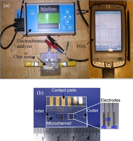
The miniaturized heavy metal lab chip sensor, as summarized in Figure 2, was made by standard microfabrication processes. The detailed microfabrication of heavy metal lab chip sensor is given elsewhere [16]. A PalmSens (Palm Instruments BV, BZ, Houten, The Netherlands) commercial portable electrochemical analyzer interfaced with a personal digital assistant (PDA) and PalmScan software was used to characterize the lab chip sensors using cyclic voltammetry (CV) and SWASV. All electrodes were electrically connected to the PalmSens commercial portable electrochemical analyzer by gold spring-loaded pins (Mill-Max Mfg. Corp., Oyster Bay, NY, USA). Generally the presence of dissolved oxygen in solution degrades the performance of cyclic voltammetric measurements, but most of the Bi-coated electrodes reported on in the literature are only negligibly affected by dissolved oxygen [17, 18]. Accordingly, our SWASV experiments were carried out without purging with pure N2 gas.
Fig. 2.
Schematic procedure of microfabrication processes for heavy metal lab chip with (a) microfluidic channel and (b) microelectrodes.
3. Results and discussion
3.1. Characterization of ion-selective lab chip sensor
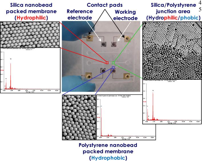
The fabrication of small size electrodes remains a prolific topic of electrochemical research. The reason is that miniaturized on-chip electrochemical sensors with planar microelectrodes would lead to numerous benefits such as greatly reducing the sensor cost due to mass production, precise control of dimensions, higher processing speed, excellent uniformity, reproducibility, making the entire sensing system portable, and very easy to use. It was also found that very small electrode dimensions are least sensitive to stirring effects in the solution [19]. The reason is that the concentration gradient exists only near the surface of the electrode; this is very useful for microfluidic chip measurements, where no stirring is possible. A novel approach here is to utilize a self-assembly Polystyrene (PS) nanobeads with hydrophobic surfaces to build the liquid ion exchange column [20] connected to a hydrophilic silica nanobeads-packed column, which is considered as one of the most difficult tasks in the development of ion-selective microelectrodes [21]. PS nanoparticles have become widely used materials since the particles are commercially available in a wide range of sizes with narrow size distribution [22]. Figure 3 shows a microphotograph of the fabricated dual ion-selective sensor chip and environmental scanning electron microscopy image of the nanobead-packed columns. In order to insure the self-assembled nanobead hetero assembly, energy dispersive spectrometry was performed over the nanobead-packed hetero assembly area as shown in Figure 3. Silicon, oxygen and carbon peaks were uniformly shown at the junction area. This clearly confirmed a heterogeneous nanobead-packed column was successfully constructed on a chip. Furthermore, excellent rate control deposition by the e-beam evaporator makes high deposition uniformity possible on any substrate and with low contamination, so that a homogeneous surface film electrode is possible, providing better performance.
Fig. 3.
Photograph of the dual ion-selective lab chip and the ESEM images with EDS data of the self-assembly nBP columns
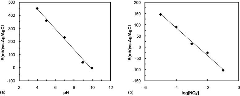
To assess the electrochemical detection performance of the ion-selective sensor chip, potentiometric responses were measured. As shown in Figure 4(a), the measured results in the variation of pH show good sensitivity with the slope of −77.031 (mV·pH−1) and good linear response within the pH range of 4–10. Figure 4(b) shows the potentiometric response of the nitrate ion-selective sensor chip was linear with a Nernstian slope of −61.369 (mV·decade−1) within the NO3 − concentration range of 10−5 to 10−1. The response times of the pH and nitrate sensors were less than 5 and 7 seconds, respectively.
Fig. 4.
Potentiometric responses of the (a) pH and (b) nitrate ion-selective lab chip.
3.2. Characterization of heavy metal lab chip sensor
It is well known that film-based electrodes exhibit good properties, provide a larger surface-to-volume ratio, offer great scope for different cell configurations, and are mechanically more stable [23]. Due to their advantages such as reproducibility of the mercury surface, the excellent negative potential range for the reduction of various heavy metal ions, faster response time, and high sensitivity [24], mercury-film electrodes (MFE), prepared by coating a suitable substrate with a thin film of metallic mercury, have recently been widely used [25, 26]. Nevertheless, because of mercury’s toxicity, expensive disposal costs are required to limit release to the environment and human exposure. On the other hand, bismuth (Bi) has the advantages of very low toxicity as opposed to mercury, and superior electrochemical properties, such as high hydrogen overpotential, relatively large applicable negative potential window (similar negative potential limit and slightly lower positive limit than that of mercury), and insensitivity to dissolved oxygen [14, 18, 27-30]. As an alternative to mercury, bismuth, a more environmentally-friendly material [28], is being considered as a working electrode, as shown in Figure 5.
Fig. 5.
Measurement system with fabricated lab chip: (a) Experiment setup for measurement of (b) cadmium, and (b) picture of the disposable heavy metal chip sensor combined with the microelectrode and microchannels.
Although an electrochemical measurement system can be designed as either a two- or three-cell system, in previous work it was reported that the three-electrode configuration in voltammetry offers more accurate measurements of the current which flows through the working electrode [31, 32]. Under this configuration, there is no danger of polarizing the Ag/AgCl reference electrode by passing the cell current (the sum of Faradic and charging current) through it, so that the reference electrode can provide stable potential under various solution compositions. Moreover, it was reported that, when the electrode size becomes smaller, the small surface area of the microelectrode could help minimize inherent background currents always present in SWASV, while yielding only small stripping currents which are vulnerable to electrical noise [33]. All electrodes used had a length of 3 mm, and a width of 0.5 mm, and a spacing of 500 μm. To carry the Faradic current generated from the results of redox reactions at the working electrode surface, the surface area of the counter electrode is equal to that of the Bi working electrode. In commercial reference electrodes, the Ag/AgCl electrode is dipped into a 1M KCl solution to keep a constant potential; in this case, though, a solid-state reference electrode was electrodeposited with a thin polymer layer containing chloride ions. The coating surface of the reference electrode is ideally reversible and nonpolarizable.
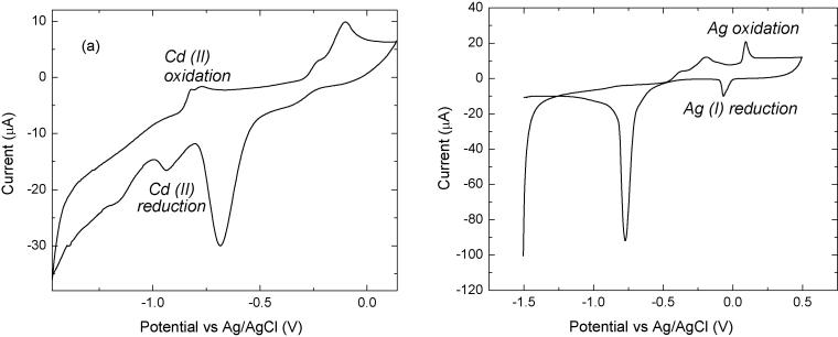
Since it is well known that the sensitivity of SWASV is significantly related to the deposition potential and time, CV was performed to find the reduction and oxidation potential of the target heavy metals using this lab chip sensor. As shown in Figure 6(a), reversible peaks of cadmium can be found at around −0.8 V and −0.9 V in the voltammograms. Thus, a potential more negative than −1.0 V is sufficient as the preconcentration potential for Cd(II) measurement. At a rather negative deposition potential of −1.2V, however, the negligible noisy current flowing through the electrode was measurable, which is due presumably to hydrogen evolution. Accordingly, a −1.2 V (versus integrated Ag/AgCl pseudo reference electrode) deposition potential was found to be the most appropriate value since replicate additions gave reproducible peak current values and the symmetry of Cd(II) peaks were confirmed at each given condition. In a few CV scans, unexpected peaks were found at potentials more positive than the Bi electrode oxidation peak, as shown in Figure 6(b). These peaks correspond to oxidation and reduction of the free Ag ions in the solution, which are generated from the disassociated Ag ions from the reference electrode due to the unsatisfied Ag/AgCl electroplating. Because the Ag/AgCl electroplating process was performed manually, it is also the major source for any chip-to-chip variation. However, since most voltammetry measurements for heavy metals are scanned at a potential range which is far more negative than the Ag standard potential, these undesired Ag peaks do not cause a significant effect on the sensing performance.
Fig. 6.
Cyclic voltammogram from the heavy metal sensor with Bi electrode in acetate buffer with 0.1 M KCl (pH=4.65) and 50 μg Cd(II) mL−1.
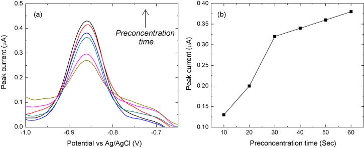
When −1.2 V was applied to start the anodic scan and the end potential was set to −0.5 V, the measured stripping currents for a 1 Cd(II) μg·mL−1 solution for several preconcentration times were as seen in Figure 7. As expected, the current peak height increased with increasing preconcentration time up to 60 sec. From these results, it was found that the output peak current is proportional to the preconcentration time. The peak current change versus the Bi electrode thickness change was also studied when measuring Cd(II) by SWASV. The thickness of the microfabricated Bi electrode can be precisely controlled by the e-beam evaporation, and it was obtained that the thicker Bi electrode generates higher output current signals in SWASV. There are two possible reasons to explain the current signal changes. One is the change in whole surface area of the electrodes. The thicker Bi electrode has a larger side area and thus increases the whole surface area of the electrode. The surface roughness of the thicker Bi film is larger and thus leads to an increase in the whole surface area. The other is the saturation of the concentrated target heavy metals inside the Bi electrode during the preconcentration step. As the target heavy metals have to penetrate into the Bi electrode body to form the low-temperature alloy with the Bi during the preconcentration step, the thinner Bi electrode may not have enough volume to form the alloy with all the concentrated heavy metals, which means the preconcentration is limited by the thickness of the Bi electrode. When the electrode thickness is large enough, all the concentrated heavy metals during the preconcentration step could penetrate into the electrode and form the alloy with Bi. The formation of the alloy is now limited by the mass of the concentrated heavy metals, and the corresponding curve becomes gradually saturated. Although thicker Bi electrode film generates higher output signal, other limitations such as the material cost and the film adhesion suggest that the electrode film thickness cannot be too large. In most of the experiments, the thickness of the microfabricated Bi electrode was 100 nm.
Fig. 7.
(a) SWASV scans at different preconcentration times while measuring 0.3 μg Cd(II) mL−1 in acetate buffer with 0.1 M KCl (pH=4.65), and (b) calibration curve.
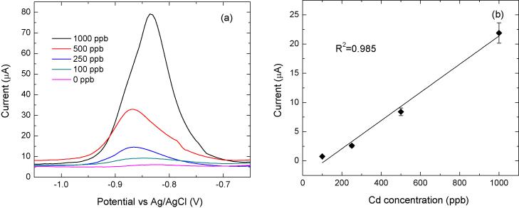
Figure 8(a) is the result of SWASV voltammograms for successive changes of Cd(II) concentrations (0-1000 μg·L−1) achieved by adding cadmium ions to DI water containing 0.1M acetate buffer and 0.1M KCl. After deposition of the Cd(II) onto the Bi working electrode at a negative potential of −1.2 V for 90 sec, the Bi microelectrode was anodically scanned over the potential range from −1.2 V to −0.5 V to strip the Cd(II) concentrated on the surface of the Bi microelectrode. As is well known, at the suitable oxidation potential of each type of metal, a rapidly increasing current peak is measured as the metal is oxidized back into solution. As a result, the height of the current peak in the stripping step is linearly proportional to the analyte concentration in solution. As shown in Figure 8(b), the Bi electrode shows a peak potential of −0.88 V, and for increased concentrations of Cd(II), the peak stripping current increased linearly (R2 = 0.985). The sensitivity is 24 nA·ppb−1. The limit of lowest detection (LOD) value of cadmium was measured to be 9.3 μg·L−1 (S·N−1 = 3). The LOD was defined as the lowest concentration of Cd(II) that is within the linear range of the calibration curve for the Cd(II) serially diluted standard solution. Up to 9.3 Cd(II) μg·L−1, it was found to be linear while at lower levels, the plot of Cd(II) concentration vs. current signal showed a deviation from linearity.
Fig. 8.
Measured Cd(II): (a) Plots are SWASV measurements of Cd(II) in acetate buffer (pH 4.65) with 0.1 M KCl (pH = 4.65), and (b) calibration curve. Conditions of SWASV for Cd(II) at Bi chip sensor are as follows; −1.2V deposition potential (Edep); 90 sec deposition time; 5mV voltage step (Estep); 25 mV amplitude (Esw); 100 Hz frequency (f); and −1.2 V to −0.5 V scan range.
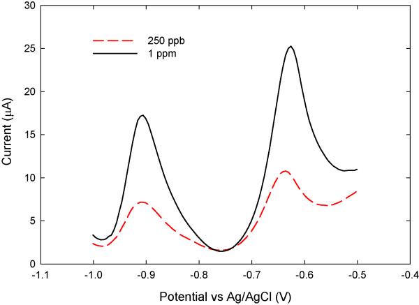
The potential interference of other heavy metal ions in the determination of cadmium by addition of Pb(II) to buffer solution was investigated under optimum conditions for measurement of Cd(II). As shown in Figure 9, Bi and the two heavy metals tested (Cd and Pb) can form an alloy that can be anodically stripped in the stripping step, resulting in well defined peaks for the two heavy metals. The potentials corresponding to the peak currents occur at − 0.85 V for Cd(II) and −0.58 for Pb(II). Due to the potential drift of the unsaturated Ag/AgCl reference electrode, there are small variations, but these values are close to their standard potentials. Also, although a small decreasing trend in anodic current was observed with the solution containing Pb(II), the disposable Bi film chip sensor does not appear to be affected by any underpotential stripping voltammetry caused by the formation of multi-component Bi alloys with numerous heavy metals [13, 24]. Accordingly, Pb(II) will probably not significantly interfere with the determination of Cd(II) in typical samples of interest.
Fig. 9.
SWASV measurements for the binary mixture of Cd(II) and Pb(II) in 0.1 M KCl acetate buffer (pH=4.65). Conditions as in Fig. 8.
4. Conclusions
As human become increasingly relied upon groundwater resources for drinking water supplies, the contamination of groundwater is an important problem; if groundwater becomes polluted, it is no longer safe to drink. However, as a result of many human activities, nitrate and heavy metals are omnipresent in soil and groundwater. Their ecotoxicological properties have been widely known for a long time. So, there is a clear need for reliable, efficient and cost-effective monitoring methods for nitrate and heavy metals that may adversely affect human health. Typical environmental sampling methods to ensure the preservation of in-situ conditions are time consuming and costly. On the other hand, the advantages of a miniaturized lab chip sensor in comparison to the conventional analytical methods mentioned above include the significantly reduced analyte consumption. In this work, an on-chip dual pH and nitrate ion-selective sensor chip has been realized using self-assembly nanobead-packed hetero columns, which provides an easy sample loading with hydrophilic silica nanobead-packed column and an ion-selective sensor with hydrophobic PS nanobeads, respectively. The nanobead-packed hetero columns provide a new electrochemical sensing platform with a high sensitivity and excellent ion selectivity with easy sampling for environmental monitoring. Furthermore, the bismuth coated film electrode is a good candidate for development of a disposable chip sensor due to the attractive electrochemical properties and environmental friendliness of the material. Accordingly, quite reliable on-site measurement of nitrate and Cd(II) penetrating into the environment is possible, which is useful for restricting environmental damage. Miniaturized environmental sensors are thus well suited for sensing, monitoring and detection of a diverse range of nitrate and heavy metals, and it can be expected that their importance will grow, especially in environmental, industrial and clinical medical diagnostics areas. To better achieve automated on-site analysis for monitoring the actual changes of pollutants, our ongoing research has focused on the integration of micro-pumps, micro-valves, and data acquisition and signal processing circuitry. The greatest potential for application of the module might be at the many Superfund and other hazardous waste sites that contain significant quantities of toxic or hazardous organics and inorganics. Further, when lower sensitivities may be acceptable for purposes of sample screening or site surveys, the module established with a relatively simple and portable setup could be applied to on site assays, because it is relatively inexpensive and can produce a large number of screening results in a short time. In our next study, therefore, we will concentrate our effort on the application of the module to these sites to monitor a variety of mixed contaminants in contaminated water.
Acknowledgements
This research was supported by a grant from the National Institute of Environmental Health Sciences (NIEHS), under the Superfund Basic Research Program (SBRP) Individual Research Projects (R01) (1R01ES015446-01) and in part by an grant from Plant Technology Advancement Program funded by Ministry of Construction & Transportation of the Korean government.
Footnotes
Publisher's Disclaimer: This is a PDF file of an unedited manuscript that has been accepted for publication. As a service to our customers we are providing this early version of the manuscript. The manuscript will undergo copyediting, typesetting, and review of the resulting proof before it is published in its final citable form. Please note that during the production process errors may be discovered which could affect the content, and all legal disclaimers that apply to the journal pertain.
References
- [1].Moore JE. Geojournal. 1983;7:453–458. [Google Scholar]
- [2].Dragon K. Water Resour Manag. 2008;22:343–355. [Google Scholar]
- [3].Sharma RK, Agrawal M. J Environ Biol. 2005;26:301–313. [PubMed] [Google Scholar]
- [4].Liu L, Lu GH. J Hydrol Eng. 2008;13:371–377. [Google Scholar]
- [5].Ju XT, Kou CL, Zhang FS, Christie P. Environ Pollut. 2006;143:117–125. doi: 10.1016/j.envpol.2005.11.005. [DOI] [PubMed] [Google Scholar]
- [6].Oenema O, Boers PCM, van Eerdt MM, Fraters B, van der Meer HG, Roest CWJ, Schroder JJ, Willems WJ. Environ Pollut. 1998;102:471–478. [Google Scholar]
- [7].Lin YF, Jing SR, Wang TW, Lee DY. Environ Pollut. 2002;119:413–420. doi: 10.1016/s0269-7491(01)00299-8. [DOI] [PubMed] [Google Scholar]
- [8].Singleton MJ, Esser BK, Moran JE, Hudson GB, Mcnab WW, Harter T. Environmental Science & Technology. 2007;41:759–765. doi: 10.1021/es061253g. [DOI] [PubMed] [Google Scholar]
- [9].Pandey PK, Verma Y, Choubey S, Pandey M, Chandrasekhar K. Bioresource Technology. 2008;99:4420–4427. doi: 10.1016/j.biortech.2007.08.026. [DOI] [PubMed] [Google Scholar]
- [10].ATSDR U.S. Department of Health and Human Services, Public Health Service; Atlanta, GA: Toxicological Profile for Cadmium. 1999
- [11].Fewtrell L. Environ Health Persp. 2004;112:1371–1374. doi: 10.1289/ehp.7216. [DOI] [PMC free article] [PubMed] [Google Scholar]
- [12].Bhattacharyya J, Read D, Amos S, Dooley S, Killham K, Paton GI. Environ Pollut. 2005;134:485–492. doi: 10.1016/j.envpol.2004.09.002. [DOI] [PubMed] [Google Scholar]
- [13].Wang J. Electroanalysis. 2005;17:1341–1346. [Google Scholar]
- [14].Baldrianova L, Svancara I, Vlcek M, Economou A, Sotiropoulos S. Electrochimica Acta. 2006;52:481–490. [Google Scholar]
- [15].Park J, Lee D, Kim W, Horiike S, Nishimoto T, Lee SH, Ahn CH. Anal. Chem. 2007;79:3214–3219. doi: 10.1021/ac061714g. [DOI] [PubMed] [Google Scholar]
- [16].Zou ZW, Jang A, MacKnight E, Wu PM, Do J, Bishop PL, Ahn CH. Sensors and Actuators B-Chemical. 2008;134:18–24. [Google Scholar]
- [17].Pauliukaite R, Hocevar SB, Ogorevc B, Wang J. Electroanalysis. 2004;16:719–723. [Google Scholar]
- [18].Wang J, Lu JM, Hocevar SB, Farias PAM, Ogorevc B. Anal Chem. 2000;72:3218–3222. doi: 10.1021/ac000108x. [DOI] [PubMed] [Google Scholar]
- [19].Pizeta I, Billon G, Fischer JC, Wartel M. Electroanalysis. 2003;15:1389–1396. [Google Scholar]
- [20].Bakker E, Buhlmann P, Pretsch E. Electroanalysis. 1999;11:915–933. [Google Scholar]
- [21].Johnson RD, Gaualas VG, Daunert S, Bachas LG. Anal Chim Acta. 2008;613:20–30. doi: 10.1016/j.aca.2008.02.041. [DOI] [PubMed] [Google Scholar]
- [22].Himmelhaus M, Takei H. Physical Chemistry Chemical Physics. 2002;4:496–506. [Google Scholar]
- [23].Economou A, Fielden PR. Analyst. 2003;128:205–212. [PubMed] [Google Scholar]
- [24].Kachoosangi RT, Banks CE, Ji XB, Compton RG. Anal Sci. 2007;23:283–289. doi: 10.2116/analsci.23.283. [DOI] [PubMed] [Google Scholar]
- [25].Tamer U, Oymak T, Ertas N. Electroanalysis. 2007;19:2565–2570. [Google Scholar]
- [26].Strbiik V, Plesch G, Chromik S, Kleja P, Kostic I, Benacka S. Supercond Sci Tech. 2002;15:1295–1299. [Google Scholar]
- [27].Gouveia-Caridade C, Pauliukaite R, Brett CMA. Electroanalysis. 2006;18:854–861. [Google Scholar]
- [28].Hocevar SB, Wang J, Deo RP, Ogorevc B. Electroanalysis. 2002;14:112–115. [Google Scholar]
- [29].Arribas AS, Bermejo E, Chicharro M, Zapardiel A. Electroanalysis. 2006;18:2331–2336. [Google Scholar]
- [30].Hocevar SB, Svancara I, Vytras K, Ogorevc B. Electrochimica Acta. 2005;51:706–710. [Google Scholar]
- [31].Yun KS, Kim HJ, Joo S, Kwak J, Yoon E. Jpn J Appl Phys 1. 2000;39:7159–7163. [Google Scholar]
- [32].Gao P, Jin XB, Wang DH, Hu XH, Chen GZ. J Electroanal Chem. 2005;579:321–328. [Google Scholar]
- [33].Chinowsky TM, Saban SB, Yee SS. Sensor Actuat B-Chem. 1996;35:37–43. [Google Scholar]


