Abstract
Visualization of atomic-scale structural motion by ultrafast electron diffraction and microscopy requires electron packets of shortest duration and highest coherence. We report on the generation and application of single-electron pulses for this purpose. Photoelectric emission from metal surfaces is studied with tunable ultraviolet pulses in the femtosecond regime. The bandwidth, efficiency, coherence, and electron pulse duration are investigated in dependence on excitation wavelength, intensity, and laser bandwidth. At photon energies close to the cathode’s work function, the electron pulse duration shortens significantly and approaches a threshold that is determined by interplay of the optical pulse width and the acceleration field. An optimized choice of laser wavelength and bandwidth results in sub-100-fs electron pulses. We demonstrate single-electron diffraction from polycrystalline diamond films and reveal the favorable influences of matched photon energies on the coherence volume of single-electron wave packets. We discuss the consequences of our findings for the physics of the photoelectric effect and for applications of single-electron pulses in ultrafast 4D imaging of structural dynamics.
Investigation of structural dynamics in condensed matter and molecules by four-dimensional imaging calls for resolution of Angstrom-scale distances with femtosecond timing. These resolutions are provided by ultrafast electron diffraction and microscopy techniques, which are based on pump–probe arrangements with a femtosecond laser for excitation and with ultrashort electron packets for measuring sequences of atomic-scale structures during changes (1). Recently reported studies include such of reaction pathways during phase transformations (2), chemical reactions (3), laser ablation (4), molecular alignment (5), changes at interfaces (6), heating and melting processes (7–9), cantilever motion (10), or evanescent fields around nanostructures (11), among many others (12). Possibilities to access the attosecond regime of charge density motion are also discussed (13), taking into account the generation of pulses (14–16) and the quantum dynamics of the scattering process (17).
These (and many more) achievements are made possible by the use of ultrashort electron packets at multi-kiloelectron-volt energies for time-resolved diffraction and imaging. Such packets can be generated by photoelectric emission from metal films illuminated with femtosecond lasers, followed by acceleration in static or radio-frequency electric fields. In multielectron packets, space-charge effects dominate the temporal structure and energy distribution; hence electron density has to be traded off against resolution (18, 19). In contrast, space charge is absent in packets containing only one single electron at a time (12). In this regime, the longitudinal and transverse emittance, and hence the pulse duration, bandwidth, and coherence, are determined by the spatiotemporal statistics of the photoelectric effect.
Some theoretical models consider the femtosecond regime of photoemission (20–22), but experimental investigations have concentrated on excitation with continuous light or picosecond pulses (23–27), or on special semiconductor materials (28). Femtosecond pulses at fixed wavelengths of 266, 400, and 800 nm were recently used on metals to study the differences between single- and multiphoton excitation (29). Here, we report an investigation of photoelectric emission with tunable femtosecond pulses from well above to below the work function. This study serves three purposes: First, the reported data reveal some femtosecond aspects of photoelectric emission in view of recent theoretical efforts (20–22). Second, we provide a recipe for generating sub-100-fs electron pulses by choosing optimized laser parameters for cathode excitation. Third, we demonstrate single-electron diffraction with these pulses and show that the coherence is sufficient for ultrafast atomic-scale imaging of complex materials.
Results
Duration of Single-Electron Pulses.
Microscopy and diffraction in the single-electron regime require accumulation of many single electrons for each pump–probe delay. The temporal resolution is therefore limited, besides optical and geometrical contributions (30), by the average timing jitter of single electrons. We therefore define the duration of single-electron packets by the temporal envelope of many distinguishable single-electron emissions with respect to a recurring time zero, which is given by the laser repetition rate (see also ref. 13 and figure 1 therein).
Single-electron generation by photoelectric emission is depicted in Fig. 1. A femtosecond laser pulse hits a thin metal layer (red) that is coated on the backside of a transparent window. Free electrons (black arrows) are generated by photoelectric emission, and a static electric field Eacc accelerates them toward and through an anode mesh (dotted line). At properly adjusted laser pulse energy, the electron packets contain, with highest probability, single electrons.
Fig. 1.
Temporal broadening in femtosecond photoelectric emission of single electrons. A laser pulse (violet) impinges on a metal cathode (red). Photoelectrons (black arrows) are generated with statistical distributions of directions and velocities. The electron pulses (blue) are temporally broadened as a result of the different trajectories of individual electrons.
From imperfect surfaces, such as the metal films used here and elsewhere, photoelectrons are generated with statistical distributions of transversal and longitudinal velocities (black arrows), because momentum transfer from photons to electrons is indirect (31, 32). In the single-electron regime, these distributions determine the longitudinal and transverse emittance, and consequently the pulse duration and divergence. Electrons with different initial speed arrive earlier or later at the anode, and the pulse shape (blue) therefore develops a temporal broadening during propagation. This is the critical effect that limits the temporal resolution of ultrafast pump–probe experiments in the absence of space charge (14, 30).
At the anode, the pulse broadening τacc is related to the spread Δvl of longitudinal velocities by
 |
[1] |
where m is the electron mass, e is the elementary charge, and Eacc is the acceleration field. Additional contributions in the region after the anode can be neglected, because the average speed at several kiloelectron volts becomes much larger than Δvl.
A common approach to minimize the electron pulse duration is to increase Eacc (2, 33, 34); this shortens the time until the electrons have reached full speed. We investigate here another approach, which is based on using tunable laser excitation at photon energies very close to the work function, in order to reduce the available excess energy and to constrain the distributions of vl and vt. This should result in lower emittance, lower energy bandwidth, and, consequently, shorter pulses. In what follows we describe the experimental arrangement, the results, and their implications for the physics of femtosecond photoemission and for ultrafast atomic-scale imaging.
Ultraviolet Laser Pulses at Tunable Photon Energy.
The work functions of metals are of the order of several electron volts. The study of femtosecond photoemission close to and also well above these thresholds therefore calls for femtosecond pulses with tunable wavelength in the UV. Fig. 2 depicts our apparatus for generating such pulses. The laser source (red) is a long-cavity Kerr-lens-mode-locked Ti:sapphire oscillator (35) operating at 5.1-MHz repetition rate and delivering 50-fs, 500-nJ pulses at a center wavelength of 800 nm. Twenty-five percent of the pulse energy is split off and focused into an yttrium/aluminum garnet (YAG) crystal for broadband continuum generation (36); the remaining 75% is available for sample excitation in case of pump–probe studies. The visible part of the continuum is focused into a β-barium-borate crystal (BBO) of 100-μm thickness for second harmonic generation (SHG). The BBO is thicker as to support the entire spectral width, and the SHG output can therefore be tuned between 240 and 350 nm by tilting the BBO crystal by ± 10°. Two special dielectric mirrors reflect only the ultraviolet contributions toward the photocathode, which consists of a 40-nm thick gold layer coated on a fused silica substrate (3 nm of chromium in-between for improving adhesion).
Fig. 2.
Generation of tunable UV femtosecond pulses. Laser pulses at 800 nm (red) are focused into a 4-mm thick YAG crystal for white light generation (WLG). The remaining 800-nm light is filtered and the continuum (green) is frequency-doubled in a BBO crystal. Two dichroic mirrors are used to reflect only the ultraviolet wavelengths. The lenses L1 - L5 have focal lengths of 50, 30, 50, 75, and 250 mm, respectively.
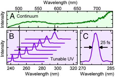
Some results are shown in Fig. 3. The continuum (Fig. 3A) covers all of the visible range and UV pulses are generated in the range of 240–300 nm (Fig. 3B). The spectra support pulse durations of about 25 fs in this range (Fig. 3C). The energy per UV pulse was measured to be on the order of 1 pJ, which corresponds to about 105–106 photons on the backside of the photocathode. The quantum efficiency (electrons per photon) of metal photocathodes is reported to be in the range of 10-5–10-7 (25, 27). In order to avoid multiple electron emission, we attenuated the UV beam in some of the experiments by moving the SHG crystal out of focus. Inside the vacuum chamber, the electrons were accelerated through an anode mesh, and the beam was recorded on a phosphor screen with a CCD camera.
Fig. 3.
Tunable UV pulses. (A) Visible part of the continuum spectrum (green). (B) Spectra of UV pulses (violet) for varying phase matching angles of the BBO crystal. (C) Details of one of the UV spectra, showing a Fourier limit of about 25 fs.
Pulse compression was not applied at the time of the presented experiments, and the UV pulses are therefore chirped. From the dispersion of all components, we estimate the pulse duration as 150–200 fs in our tuning range. Such chirp is not significant for the following investigations of velocity spreads in the single-electron regime, because no direct temporal measurement is applied. For pump–probe studies, however, the UV pulses must be compressed, e.g., with chirped multilayer mirrors (37, 38).
Measurement of Transverse Velocity Spreads.
The physics of photoelectric emission can be described with three essential steps (20, 31): First, a photon is absorbed and excites an electron within the cathode material. Second, electron–electron and other interactions with the material may occur during propagation toward the surface. Third, those electrons with still enough energy can escape the crystal potential and are ejected into free space. For metal cathodes with imperfect surfaces, the emission exhibits a fairly isotropic angular distribution into a half sphere. Thermal effects, refraction from the inside to the outside of the crystal potential, and surface roughness all tend to reduce possible anisotropic contributions.
The transverse velocity spread of photoelectrons can be determined by measurements of the electron beam diameter (29). The trajectory of an electron with a transverse velocity vt (see Fig. 1) consists of a parabolic path as result of the acceleration voltage Uacc in the cathode–anode region (Lacc) and a linear propagation afterward in the field-free region (Ldrift). The longitudinal velocity component vl is negligible here, because the forward velocity induced by acceleration is higher by many orders of magnitude. Also, the radius of the emitting area, R0, which is determined by the optical focus, can be neglected, as shown below. As a result, the point of incidence on the screen, R, is proportionally related to the transverse velocity vt of single photoelectrons. A distribution of transverse velocities Δvt then results in a distribution on the screen, of which the radius ΔR is given by
 |
[2] |
The beam profile averaged over many single-electron events therefore displays the transverse velocity distribution of photoelectrons under the respective excitation conditions.
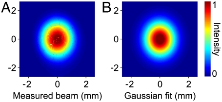
Fig. 4A shows a typical measured beam profile, which comprises ∼108 single-electron events. An electron energy of 24 keV and an acceleration field of 1 kV/mm were used. The rather low field strength, which is only 10% of the value we use for pump–probe studies, minimizes the influence of the Schottky effect in changing the work function. We calculated that the local temperature increase caused by absorption of one UV pulse is less than 0.1 K, and less than 1 K on average. Impulsive heating and thermionic emission are therefore negligible, and the reported results are from direct photoelectric emission only.
Fig. 4.
Comparison of measured (A) and fitted (B) electron beam profiles.
Through our optical tuning range, the beam profiles on the screen at a distance of about 300 mm have diameters in the millimeter range. As expected for an isotropic emission, almost Gaussian shapes (see Fig. 4A) are observed at all wavelengths. This excludes a significant change of the spatial emission characteristics with changing photon energy. The spot widths are determined by two-dimensional fitting (Fig. 4B). When tuning the photon energy from above to close to the work function, a significant narrowing is observed.
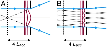
Concluding from the beam radius ΔR to the velocity spread Δvt requires the elimination of several possible systematic influences, which we briefly discuss. First, we exclude the presence of space charge by recording the beam diameter at constant photon energy in dependence of the UV laser power. A reduction by a factor of 100 did not change the beam diameter, as expected. Second, we consider the inhomogeneous penetration of electric fields into the anode’s aperture, which forms a negative lens. The effective focal length of 4Lacc is approximately independent of the aperture size (15). Fig. 5A depicts the lens effect for an anode with a millimeter-sized hole (black), which is usually applied in our diffraction experiments, and for the case of a dense mesh, which was used for these experiments (Fig. 5B). The defocusing effect (dotted lines) has a similar focal length in both cases, but the mesh widens the overall beam (blue) much less as a result of the many small holes. For Lacc ≈ 25 mm, and a mesh opening of about 80 μm, the beam radius on the screen increases by less than 130 μm, which is negligible as compared to the much larger beams resulting from electron statistics. A third contribution to the measured beam diameter may come from the optical focus size on the cathode. From optical modeling we derive a spot radius of < 25 μm in the range of 240–300 nm; this is negligible.
Fig. 5.
Influence of field penetration (magenta) for different types of acceleration elements. (A) Anode with a hole; (B) anode with a mesh. The mesh induces only an insignificant divergence (see text).
In order to further support the above conclusions, we measured the beam diameter as a function of the acceleration voltage. When scanning Uacc for a constant photon energy, the beam radius on the screen changes according to Eq. 2 with a characteristic inverse square root law; any deviations thereof would indicate geometric contributions that are independent of Uacc. A fit of Eq. 2, but allowing for a systematic contribution R0 to the beam radius, results in a value of R0 < 150 μm. This is an experimental upper limit for the combined contributions of detector resolution, mesh defocusing, optical spot size, and other effects. In relation to the millimeter-sized electron beam diameters, this contribution is insignificant.
Photoemission with Tunable Excitation.
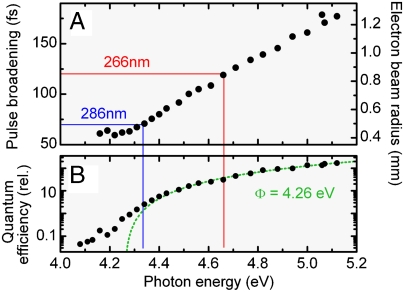
Considering these supporting measurements, we can now evaluate the photoemission characteristics as a function of the photon energy. The results are shown in Fig. 6. Fig. 6B, Lower, shows the relative electron yield (quantum efficiency, electrons per photon) on a logarithmic scale. Toward lower photon energies, the quantum efficiency of the photoemission process decreases sharply, which is expected because less of the electrons initially excited inside the cathode material have enough energy to escape the crystal potential. In order to determine the effective work function of our material, we use the data above 4.4 eV and apply a quadratic dependence (20) (green). The effective work function for our gold cathode is Φ = 4.26 ± 0.05 eV, corresponding to a cutoff wavelength of 291 nm. This value is very robust against the particular choice of fitting ranges (> 4.3, > 4.4, or > 4.5 eV) and corresponds well to previously reported values for amorphous gold layers (25).
Fig. 6.
Photoelectron statistics and quantum efficiency for tunable excitation. (A) A significant shrinking of the beam radius is observed toward lower excitation energies. The left scale provides the temporal broadening of electron pulses assuming an acceleration field of 10 kV/mm (see text). The red and blue lines denote conventional and optimized excitation wavelengths. (B) Quantum efficiency (electrons per photon, relative) in dependence of the photon energy (dots).
Excitation at photon energies below the work function shows significantly more electrons than expected from the Fermi statistics at room temperature. This results from the large optical bandwidth of our femtosecond UV pulses, which have some spectral components quite far off the central wavelength (see the characteristic sinc2-shaped spectrum with side maxima, Fig. 3C). The optical bandwidth is effectively truncated and only the part below the cutoff wavelength contributes to photoemission. The rest of the laser spectrum is lost to carrier excitations that do not lead to photoemission. An experimental evidence for this behavior is the approximately exponential decrease of the electron yield below the work function, following the shape of the optical spectrum.
Fig. 6A shows the beam radius. Toward lower photon energies, the beam is narrowing by a factor of three over our tuning range, due to a decreasing excess energy of the photoelectrons. We note that the minimum beam radius of about 0.4 mm at the cutoff wavelength (291 nm) is not limited by systematic contributions or detector resolution. Consequently, even at photon energies matching the work function, there is a significant residual uncertainty of the photoelectron velocity distribution. This important observation is discussed below.
In order to infer the longitudinal expansion, i.e., temporal broadening of the electron pulse, from our measurement of transverse velocity components Δvt (see Eq. 2), the longitudinal velocity spread Δvl must be derived (see Eq. 1). To this end, we assume an isotropic emission of the cathode with equal emission probabilities into the half sphere. This is justified by the rather rough surface and the tilted facets of our gold films, which were coated on amorphous silica substrates. With these assumptions we obtain
| [3] |
Note that this relation can depend on the particular distribution of absolute values for the isotropic velocity vectors, but such dependence is numerically found to change Eq. 3 by less than ± 20% for realistic distributions. By obtaining Δvt from the beam radius, we can then calculate the electron pulse broadening τacc as a function of excitation photon energy (see left scale in Fig. 6A). These results are derived from the measured transverse spread (right scale in Fig. 6A) under the assumption of Eacc = 10 kV/mm, a static field close to the vacuum breakdown.
When tuning the excitation wavelength from the usual excitation at 266 nm (red lines) to, for example, 286 nm (blue lines), the electron pulse broadening is reduced to about 70 fs. This marks a significant improvement over conventional sources of electron pulses, where temporal broadening was reported in the 150- to 300-fs regime (14, 18, 29, 33). In spite of the lower quantum efficiency at 286 nm, single or a few electrons per pulse can still be generated with our optical UV source.
The electron broadening times inferred from our measurements of velocity spreads may somewhat depend on the assumptions made, but a relative pulse shortening trend at excitation close to the work function is evident from our data. Temporal pulse characterization with few-femtosecond resolution will be an essential task for the future (39). We note that the electron pulse durations reported in ref. 33 for two-photon excitation at 500 nm can be extrapolated to the regime of no space charge and correspond reasonably to the pulse durations we calculate for single-photon excitation at 250 nm. This agreement corroborates our methodology for assessing the time scale depicted in Fig. 6.
Optimum Laser Bandwidth at Threshold.
The final electron pulse duration τelectron is a convolution of the optical pulse duration τlaser with the temporal electron broadening τacc:
 |
[4] |
We note that photoelectric emission itself is almost instantaneous in metals (40), because the effective emission layer is constrained to a thickness of a few nanometers as a result of the short electron–electron scattering length. Close to the work function, the residual energy spread of the photoelectrons, and thereby their broadening, is dictated by the excitation energy bandwidth of the laser. This implies that there is an optimum excitation pulse duration/bandwidth for achieving the shortest electron pulses.
In order to find this optimum, we relate the measured transverse velocity spread to an effective energy bandwidth ΔE of the photoelectrons (see Materials and Methods):
 |
[5] |
The temporal broadening τacc of the accelerated photoelectron pulse is then given by
 |
[6] |
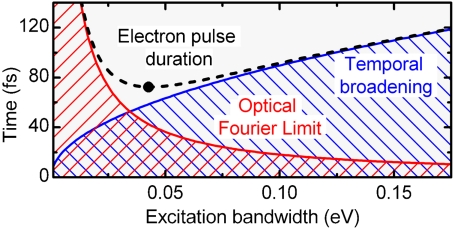
This relation is plotted in Fig. 7, blue trace. The more bandwidth, the longer the electron pulses. On the other hand, the duration of an optical pulse (Gaussian shape) with an energy bandwidth ΔE can have only a minimum Fourier-limited duration of
 |
[7] |
Fig. 7.
Limitations for achievable electron pulse durations derived from uncertainty considerations. Red: Fourier limit of Gaussian laser pulses. Blue: temporal electron broadening, assuming acceleration at 10 kV/mm. Dashed line: final electron pulse duration. Dot: optimum conditions; no shorter pulses can be generated (see text).
This relation is plotted in Fig. 7, red trace. The shorter the optical pulse, the larger its bandwidth. The convolution of both traces according to Eq. 4 yields the resulting electron pulse duration (dashed line) in dependence of the excitation bandwidth. The minimum of this trace (dot) denotes the optimum optical excitation bandwidth required for generating the shortest single-electron pulses at the output of a static accelerator. For a static field of Eacc = 10 kV/mm (limited by vacuum breakdown), the shortest possible electron pulse duration is about 70 fs (dot). The laser pulses required for this are centered just above the work function and have a duration of about 40 fs.
For different acceleration fields, the dependence of the optimum laser pulse duration τopt is calculated by inserting Eqs. 6 and 7 into Eq. 4 and finding the minimum:
 |
[8] |
This relation gives a recipe for synthesizing laser pulses of optimum duration for a given static field. For example, τopt ≈ 40 fs for Eacc = 10 kV/mm and τopt ≈ 60 fs for Eacc = 6 kV/mm.
In the experiment, we generated UV pulses of different bandwidth by changing the phase matching bandwidth of the BBO crystal used for SHG. By using BBO crystals of 25-, 100-, 200-, and 300-μm thickness, the spectral widths Δλ of the UV pulses were adjusted in the range of 2–10 nm, corresponding to optical Fourier limits of 10–60 fs. At a central wavelength of 266 nm, which is quite far from the work function, we observed no change of the electron beam when changing the bandwidth. Photoelectrons generated far above the work function have energy distributions ranging all the way from zero to the photon energy, and the laser bandwidth is therefore an insignificant contribution. In contrast, at the cutoff wavelength of 291 nm, we measured a narrowing of the electron beam by about 10% through the range of Δλ = 2–10 nm. This trend, in combination with the independence at 266 nm, shows that the laser bandwidth indeed requires optimization at excitation energies close to the work function, in order to generate the shortest electron packets.
Coherence of Single-Electron Beams.
Ultrafast diffraction is an interference process, and electrons are scattered individually from the sample’s atoms as quantum wave packets (17, 18). On the detector, each electron interferes with itself and generates an event with highest probability at the positions of diffraction features and unlikely in-between. Accumulated diffraction patterns with single-electron packets are therefore similar to such obtained with multielectron pulses, if the total number of electrons is the same.
The ability of electrons to spatially resolve atomic distances and their changes depends critically on the scales of coherence within the packets. Only such scatterers that lie within the coherence volume of the electron packets can contribute to the contrast of a diffraction pattern. The minimum transversal and longitudinal coherence lengths Lt and Ll of an electron beam are given by Lt ≈ ℏ/(meΔvt) and Ll ≈ ℏv0/(2ΔE) (18, 41, 42); v0 is the mean longitudinal velocity of the accelerated packet. Assuming that our beams are described by these limits, the reported improvements of velocity spread and energy bandwidth at photon energies close to the work function should, besides improving temporal resolution, also enhance the coherence and interference contrast of single-electron diffraction patterns.
In order to investigate this relation, we studied the sharpness of diffraction features in dependence of the photocathode’s excitation conditions. The same optical scheme as described above was applied, but a magnetic lens was applied about 5 cm behind the anode mesh. Without a condenser or pinhole, the beam was almost collimated and had diameters of about 350 μm at the sample and at the detector (this time at a distance of about 80 cm).
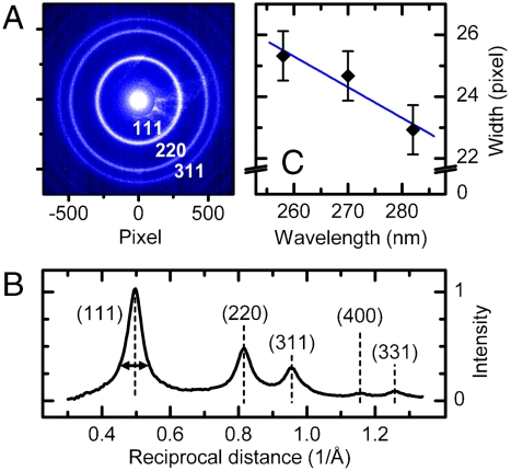
Fig. 8A shows an experimental diffraction pattern of a freestanding polycrystalline diamond film of 50-nm thickness. The ring structure is the result of Bragg diffraction from randomly oriented crystallites within the film. Diamond was selected for this study, because many Bragg reflections are forbidden and the observed diffraction rings are therefore well separated. The shown image is an accumulation of about 109 single-electron events (about 10-min integration); this demonstrates the ability of each individual electron to interfere with itself, as outlined above. Fig. 8B shows the radial intensity distribution and the Miller indices of diamond’s Bragg reflections; some smooth background contributions were subtracted for clarity.
Fig. 8.
Single-electron diffraction and effects of wave-packet coherence. (A) Diffraction pattern of a polycrystalline diamond foil. (B) Radial intensity distribution. (C) Width of the (111) diffraction ring in dependence of the photocathode excitation wavelength.
A limited coherence of the electron packets broadens the rings, because only a limited number of unit cells in the crystallites can contribute to diffraction. At multi-kiloelectron-volt energies, the broadening depends almost only on the transversal coherence length, and the longitudinal coherence is almost irrelevant as a consequence of the small scattering angles (41). The width of crystalline diffraction features is therefore a measure of the transversal coherence length Lt. In the experiment, the width is additionally broadened by the detector resolution and by the beam diameter on the screen. We therefore used the direct beam’s profile to deconvolute the measured ring widths, in order to selectively evaluate the broadening contribution originating from the limited coherence in our single-electron packets.
Fig. 8C shows the results for the (111) diffraction ring in dependence of the excitation laser wavelength. A narrowing is observed for excitation closer to the work function. This tendency shows that the transversal coherence of single electrons increases for lower excess energies. We note that inelastic loss, multiple scattering, and the unknown distribution of crystallite sizes in the diamond film may also contribute significantly to broadening the diffraction rings. Such influences are independent of the cathode’s excitation mechanisms and add a constant to the ring width at all wavelengths. The reported trend is therefore a lower limit, and the actual coherence of the electron packets may increase more than measured here.
Two observations of this study are most important for us: First, the coherence of single-electron pulses is sufficient to image rather complex unit cells and molecules. From the ring width in Fig. 8, we evaluate a transversal coherence of about 2.5 nm or better. By considering the measured Δvt and the about threefold magnification of the source’s image at the sample by the magnetic lens, we obtain Lt ≈ 3 nm, which matches reasonably. Our single-electron packets are therefore found appropriate for studying rather large atomic distances without having to reduce the electron current by a pinhole or condenser. Second, the coherence width is improving at excitation closer to the work function. This supports our statistical picture of photoelectric emission and the connection between velocity spread and coherence. Tunable excitation is a method for decreasing the packet duration and increasing the coherence volume at the same time.
Discussion
The reported results reveal the significant role of the excitation photon energy for the bandwidth, coherence, and duration of femtosecond single-electron pulses. Tunable UV excitation close to the work function, optimization of laser bandwidth, and avoidance of space charge by single-electron emission are combined to generate electron pulses shorter than 100 fs. This marks the breach of an important barrier for ultrafast atomic-scale imaging, in view of ultrafast processes such as coherent vibrations or reaction pathways on energy landscapes. The reported diffraction patterns show that, at megahertz repetition rates, ultrafast single-electron diffraction at sub-100-fs resolution is practically possible.
We also perceive some value of our results for other research fields. First, the measured dependencies are significant observations for advancing theoretical models of photoelectric emission to include the femtosecond scale. Emittance and quantum efficiency have opposing dependencies on excitation wavelength; this confirms some recent theoretical predictions with relevance to electron accelerators (21). The interplay of laser parameters and surface morphology defines the initial phase space of photoemission. Second, the provided data and relations shall be useful for energy-filtered diffraction and microscopy (43, 44), femtosecond needle sources (45, 46), propagation of elliptical packets (47), and for electron pulse compression with time-dependent fields (2, 14, 15, 17). The outlined measurement approach is a practical way to investigate and optimize the energetic, temporal, and spatial characteristics of femtosecond electron packets for these and other applications. Third, the reported optical source of widely tunable femtosecond UV pulses has potential for general application, for example, for ultrafast pump–probe experiments, two-dimensional spectroscopy, or material processing. The scheme’s simplicity and stability have already made it a standard approach in our laboratory for various purposes.
Most important for our aim of dynamical atomic- and subatomic imaging with ultimate resolutions is the successful demonstration of single-electron diffraction with packets of, assuming optical chirp compensation, sub-100-fs duration. These achievements will allow us to study the fastest and most primary processes of atomic rearrangements with 4D electron diffraction.
Materials and Methods
Here we provide the details for deriving Δvt from ΔE (Eq. 5). The momentum distributions of photons and photoelectrons are not directly related, because the photoemission process is statistical and involves scattering, many-body processes, and refraction from rough surfaces (31, 32, 48). We model the electron energy by a Gaussian distribution (29) with a bandwidth ΔE (width at half maximum):
 |
[9] |
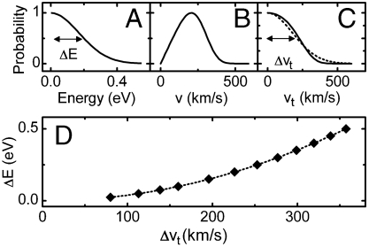
An example of such distribution with ΔE = 0.2 eV is plotted in Fig. 9A. For the distribution of the absolute velocities v within the initial photoelectron cloud we obtain
 |
[10] |
Fig. 9.
Relation of photoelectron energy bandwidth and velocity spread. (A) Gaussian distribution of photoelectrons with a width ΔE. (B) Absolute velocities. (C) Distribution of transversal velocity components (solid line). The shape is approximately Gaussian (dashed line) and corresponds to Gaussian electron beams on the screen. (D) Relation of the energy bandwidth and the transversal velocity spread (see text).
The result is plotted in Fig. 9B; note that the width of  does not directly correspond to the width ΔE. Assuming an isotropic emission, we can derive the distribution of the transversal velocity components vt:
 |
[11] |
The evaluation of this distribution requires numerical integration. The result is shown in Fig. 9C for the example of ΔE = 0.2 eV. Note that the resulting curve is close to Gaussian and the use of Gaussian fits for the experimental beam profiles is therefore justified. The width of  is plotted in Fig. 9D in relation to the energy bandwidth ΔE. The apparent quadratic dependency can be fitted and approximately be described by
  ; this is Eq. 5. An error of about 5% is accepted here in order to replace the numerical fitting constant by the more convenient
  , which facilitates the subsequent calculations. The influence of a possible nonisotropic emission (49) was also considered in the same way. Some constants are different in such cases, but the general dependencies, orders of magnitude, and the evaluation of relative trends for pulse durations are not affected.
Acknowledgments.
This work was supported by the Rudolf-Kaiser-Stiftung, the Munich-Centre for Advanced Photonics, and the European Research Council. F.O.K. is supported by the International Max Planck Research School of Advanced Photon Science.
Footnotes
The authors declare no conflict of interest.
This article is a PNAS Direct Submission.
References
- 1.Shorokhov D, Zewail AH. New light on molecular and materials complexity: 4D electron imaging. J Am Chem Soc. 2009;131:17998–18015. doi: 10.1021/ja907432p. [DOI] [PubMed] [Google Scholar]
- 2.Baum P, Yang DS, Zewail AH. 4D visualization of transitional structures in phase transformations by electron diffraction. Science. 2007;318:788–792. doi: 10.1126/science.1147724. [DOI] [PubMed] [Google Scholar]
- 3.Ihee H, et al. Direct imaging of transient molecular structures with ultrafast diffraction. Science. 2001;291:458–462. doi: 10.1126/science.291.5503.458. [DOI] [PubMed] [Google Scholar]
- 4.Carbone F, Baum P, Rudolf P, Zewail AH. Structural preablation dynamics of graphite observed by ultrafast electron crystallography. Phys Rev Lett. 2008;100:035501. doi: 10.1103/PhysRevLett.100.035501. [DOI] [PubMed] [Google Scholar]
- 5.Reckenthaeler P, et al. Time-resolved electron diffraction from selectively aligned molecules. Phys Rev Lett. 2009;102:213001. doi: 10.1103/PhysRevLett.102.213001. [DOI] [PubMed] [Google Scholar]
- 6.Yang DS, Zewail AH. Ordered water structure at hydrophobic graphite interfaces observed by 4D, ultrafast electron crystallography. Proc Natl Acad Sci USA. 2009;106:4122–4126. doi: 10.1073/pnas.0812409106. [DOI] [PMC free article] [PubMed] [Google Scholar]
- 7.Ernstorfer R, et al. The formation of warm dense matter: Experimental evidence for electronic bond hardening in gold. Science. 2009;323:1033–1037. doi: 10.1126/science.1162697. [DOI] [PubMed] [Google Scholar]
- 8.Raman RK, et al. Electronically driven fragmentation of silver nanocrystals revealed by ultrafast electron crystallography. Phys Rev Lett. 2010;104:123401. doi: 10.1103/PhysRevLett.104.123401. [DOI] [PubMed] [Google Scholar]
- 9.Wang X, et al. Electronic Grüneisen parameter and thermal expansion in ferromagnetic transition metal. Appl Phys Lett. 2008;92:121918. [Google Scholar]
- 10.Flannigan DJ, Samartzis PC, Yurtsever A, Zewail AH. Nanomechanical motions of cantilevers: Direct imaging in real space and time with 4D electron microscopy. Nano Lett. 2009;9:875–881. doi: 10.1021/nl803770e. [DOI] [PubMed] [Google Scholar]
- 11.Barwick B, Flannigan DJ, Zewail AH. Photon-induced near-field electron microscopy. Nature. 2009;462:902–906. doi: 10.1038/nature08662. [DOI] [PubMed] [Google Scholar]
- 12.Zewail AH. Four-dimensional electron microscopy. Science. 2010;328:187–193. doi: 10.1126/science.1166135. [DOI] [PubMed] [Google Scholar]
- 13.Baum P, Zewail AH. 4D attosecond imaging with free electrons: Diffraction methods and potential applications. Chem Phys. 2009;366:2–8. [Google Scholar]
- 14.Fill E, Veisz L, Apolonski A, Krausz F. Sub-fs electron pulses for ultrafast electron diffraction. New J Phys. 2006;8:272. [Google Scholar]
- 15.Veisz L, et al. Hybrid dc-ac electron gun for fs-electron pulse generation. New J Phys. 2007;9:451. [Google Scholar]
- 16.Baum P, Zewail AH. Attosecond electron pulses for 4D diffraction and microscopy. Proc Natl Acad Sci USA. 2007;104:18409–18414. doi: 10.1073/pnas.0709019104. [DOI] [PMC free article] [PubMed] [Google Scholar]
- 17.Baum P, Manz J, Schild A. Quantum model simulations of attosecond electron diffraction. Sci China Ser G. 2010;53:987–1004. [Google Scholar]
- 18.Gahlmann A, Park ST, Zewail AH. Ultrashort electron pulses for diffraction, crystallography and microscopy: Theoretical and experimental resolutions. Phys Chem Chem Phys. 2008;10:2894–2909. doi: 10.1039/b802136h. [DOI] [PubMed] [Google Scholar]
- 19.Siwick BJ, Dwyer JR, Jordan RE, Miller RJD. Ultrafast electron optics: Propagation dynamics of femtosecond electron packets. J Appl Phys. 2002;92:1643–1648. [Google Scholar]
- 20.Dowell DH, Schmerge JF. Quantum efficiency and thermal emittance of metal photocathodes. Phys Rev ST Accel Beams. 2009;12:074201. [Google Scholar]
- 21.Jensen KL, Moody NA, Feldman DW, Montgomery EJ, O’Shea PG. Photoemission from metals and cesiated surfaces. J Appl Phys. 2007;102:074902. [Google Scholar]
- 22.Wu L, Ang LK. Nonequilibrium model of ultrafast laser-induced electron photofield emission from a dc-biased metallic surface. Phys Rev B. 2008;78:224112. [Google Scholar]
- 23.Hauri CP, et al. Intrinsic emittance reduction of an electron beam from metal photocathodes. Phys Rev Lett. 2010;104:234802. doi: 10.1103/PhysRevLett.104.234802. [DOI] [PubMed] [Google Scholar]
- 24.Dowell DH, King FK, Kirby RE, Schmerge JF, Smedley JM. In situ cleaning of metal cathodes using a hydrogen ion beam. Phys Rev ST Accel Beams. 2006;9:063502. [Google Scholar]
- 25.Jiang X, Berglund CN, Bell AE, Mackie WA. Photoemission from gold thin films for application in multiphotocathode arrays for electron beam lithography. J Vac Sci Technol B. 1998;16:3374–3379. [Google Scholar]
- 26.Srinivasan-Rao T, Fischer J, Tsang T. Photoemission studies on metals using picosecond ultraviolet laser pulses. J Appl Phys. 1991;69:3291–3296. [Google Scholar]
- 27.Krolikowski WF, Spicer WE. Photoemission studies of the noble metals. II. Gold. Phys Rev B. 1970;1:478–487. [Google Scholar]
- 28.Bazarov IV, et al. Thermal emittance and response time measurements of negative electron affinity photocathodes. J Appl Phys. 2008;103:054901. [Google Scholar]
- 29.Wytrykus D, et al. Ultrashort pulse electron gun with a MHz repetition rate. Appl Phys B. 2009;96:309–314. [Google Scholar]
- 30.Baum P, Zewail AH. Breaking resolution limits in ultrafast electron diffraction and microscopy. Proc Natl Acad Sci USA. 2006;103:16105–16110. doi: 10.1073/pnas.0607451103. [DOI] [PMC free article] [PubMed] [Google Scholar]
- 31.Spicer WE. Optical transitions in which crystal momentum is not conserved. Phys Rev Lett. 1963;11:243–245. [Google Scholar]
- 32.Spicer WE. Possible non-one-electron effects in the fundamental optical excitation spectra of certain crystalline solids and their effect on photoemission. Phys Rev. 1967;154:385–394. [Google Scholar]
- 33.Hebeisen CT, et al. Grating enhanced ponderomotive scattering for visualization and full characterization of femtosecond electron pulses. Opt Express. 2008;16:3334–3341. doi: 10.1364/oe.16.003334. [DOI] [PubMed] [Google Scholar]
- 34.Musumeci P, et al. High quality single shot diffraction patterns using ultrashort megaelectron volt electron beams from a radio frequency photoinjector. Rev Sci Instrum. 2010;81:013306. doi: 10.1063/1.3292683. [DOI] [PubMed] [Google Scholar]
- 35.Naumov S, et al. Approaching the microjoule frontier with femtosecond laser oscillators. New J Phys. 2005;7:216. [Google Scholar]
- 36.Bradler M, Baum P, Riedle E. Femtosecond continuum generation in bulk laser host materials with sub-μJ pump pulses. Appl Phys B. 2009;97:561–574. [Google Scholar]
- 37.Baum P, Breuer M, Riedle E, Steinmeyer G. Brewster-angled chirped mirrors for broadband pulse compression without dispersion oscillations. Opt Lett. 2006;31:2220–2222. doi: 10.1364/ol.31.002220. [DOI] [PubMed] [Google Scholar]
- 38.Pervak V, Ahmad I, Trubetskov MK, Tikhonravov AV, Krausz F. Double-angle multilayer mirrors with smooth dispersion characteristics. Opt Express. 2009;17:7943–7951. doi: 10.1364/oe.17.007943. [DOI] [PubMed] [Google Scholar]
- 39.Reckenthaeler P, et al. Proposed method for measuring the duration of electron pulses by attosecond streaking. Phys Rev A. 2008;77:042902. [Google Scholar]
- 40.Cavalieri AL, et al. Attosecond spectroscopy in condensed matter. Nature. 2007;449:1029–1032. doi: 10.1038/nature06229. [DOI] [PubMed] [Google Scholar]
- 41.Michalik AM, Sherman EY, Sipe JE. Theory of ultrafast electron diffraction: The role of the electron bunch properties. J Appl Phys. 2008;104:054905. [Google Scholar]
- 42.van Oudheusden T, et al. Electron source concept for single-shot sub-100 fs electron diffraction in the 100 keV range. J Appl Phys. 2007;102:093501. [Google Scholar]
- 43.Baum P, Zewail A. Femtosecond diffraction with chirped electron pulses. Chem Phys Lett. 2008;462:14–17. [Google Scholar]
- 44.Carbone F, Kwon OH, Zewail AH. Dynamics of chemical bonding mapped by energy-resolved 4D electron microscopy. Science. 2009;325:181–184. doi: 10.1126/science.1175005. [DOI] [PubMed] [Google Scholar]
- 45.Hommelhoff P, et al. Extreme localization of electrons in space and time. Ultramicroscopy. 2009;109:423–429. doi: 10.1016/j.ultramic.2008.10.021. [DOI] [PubMed] [Google Scholar]
- 46.Hilbert SA, Neukirch A, Uiterwaal CJGJ, Batelaan H. Exploring temporal and rate limits of laser-induced electron emission. J Phys B. 2009;42:141001. [Google Scholar]
- 47.van der Geer SB, et al. Longitudinal phase-space manipulation of ellipsoidal electron bunches in realistic fields. Phys Rev ST Accel Beams. 2006;9:044203. [Google Scholar]
- 48.Jensen KL, et al. Application of a general electron emission equation to surface nonuniformity and current density variation. J Vac Sci Technol B. 2008;26:831–837. [Google Scholar]
- 49.Pei Z, Berglund CN. Angular distribution of photoemission from gold thin films. Jpn J Appl Phys. 2002;41:L52–L54. [Google Scholar]


