Abstract
We present the Molecular Beam Epitaxy fabrication of complex GaAs/AlGaAs nanostructures by Droplet Epitaxy, characterized by the presence of concentric multiple rings. We propose an innovative experimental procedure that allows the fabrication of individual portions of the structure, controlling their diameter by only changing the substrate temperature. The obtained nanocrystals show a significant anisotropy between [110] and [1–10] crystallographic directions, which can be ascribed to different activation energies for the Ga atoms migration processes.
Keywords: GaAs/AlGaAs, Molecular beam epitaxy, Droplet epitaxy, Quantum rings
Introduction
In recent times, Droplet Epitaxy (DE) [1,2] has extensively been used for the fabrication of III–V semiconductor quantum nanostructures that show a good rotational symmetry. Indeed with this MBE-based technique, many different quantum systems with cylindrical symmetry can be grown, ranging from quantum rings (QRs) [3,4], to concentric multiple quantum rings (CMQRs) [5], to coupled rings/disks (CRDs) [6]. The interest in fabricating such structures is both fundamental, for the investigation of quantum interference phenomena [7,8] and practical, in the fields of optoelectronics [9] and quantum information technology [10]. In GaAs DE, the fabrication of the compound semiconductor is basically achieved in two steps: first, Ga molecular beam is supplied on the substrate in absence of As, for the formation of nanometre-size droplets and then, an As flux is used to transform the droplets into GaAs. Depending on the conditions of the crystallization step, many different shapes of the GaAs nanocrystals can be obtained. In particular, caused by the surface migration of Ga atoms from the originally formed droplet during the As molecular beam supply, a lateral growth of GaAs will be observed, which gives rise to the formation of outer rings or disks. By exploiting this lateral growth, here we propose a fabrication method for the formation of GaAs concentric multiple rings, based on sequential short-time (few tenth of seconds) As molecular beam supplies at different substrate temperatures. Compared to the standard DE, the innovation of our growth protocol consists in supplying only a small amount of As atoms to achieve a partial crystallization of the available Ga, which is stored in the droplets; after changing the substrate temperature, the procedure is repeated.
Experimental Details
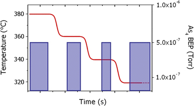
The growth experiments were performed on epi-ready GaAs (001) wafers in a standard GEN II MBE system, equipped with a Reflection High Energy Electron Diffraction (RHEED) system, for the in situ monitoring of the growth. For a good control of the As flux, a valved cell was used, which provided As4 molecules. Initially, a GaAs buffer layer and an Al0.3Ga0.7As barrier layer were grown at around 580°C, after the oxide desorption. The substrate temperature was then decreased to 400°C, and the Arsenic partial pressure in the chamber reduced below 1 × 10⁻⁹ Torr order. At this point equivalent, 30 MLs of Ga were supplied to form Ga droplets with a deposition rate of 0.02 ML/s. Four crystallization steps were then performed, by using the same As flux of 5 × 10⁻⁷ Torr at different temperatures: at 380°C for 90 s, at 360°C for 60 s, at 340°C for 45 s and finally at 320°C for 10 min in order to ensure the complete crystallization. Figure 1 schematically shows the experimental procedure used in this experiment. It is worth mentioning that in this case the substrate temperature sequence starts from the highest value (380°C), while in our recent fabrication method for CMQRs [5], we used a reverse sequence, starting from the lowest temperature.
Figure 1.

Scheme of the experimental procedure followed in our experiment. Substrate temperature (red line) and arsenic supplies (blue rectangles) are plotted as a function of time
Just after the growth, the sample was cooled at room temperature and the surface morphology was investigated by means of Atomic Force Microscopy (AFM).
Results and Discussion
After the procedure of Ga molecular beam supply, numerous nearly hemispherical Gallium droplets were formed, with an average diameter of around 160 nm and a density of around 1 × 108 cm−2. The size distribution of the Ga droplets is estimated to be around 10%. After the crystallization procedure, well-defined GaAs multiple ring structures appeared. It is worth noticing that inner ring diameter is nearly equal to that of the original Ga droplet and that the density of the GaAs structures is equal to that of the original droplets, confirming that all Ga droplets transformed into GaAs multiple rings at the end of the procedure.
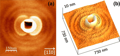
In Fig. 2, we show the AFM images of a single concentric multiple rings structure obtained after the above mentioned experimental procedure. Five concentric nanometre-size GaAs rings are clearly formed at the end of the procedure and even if the rings generally show a good rotational symmetry, some degree of anisotropy is surely present and more emphasized for the inner rings. This anisotropy might arise from the different surface migration length of Ga atoms along [1–10] and [110]. The rings diameter along [1–10] direction are 150, 350, 430, 550 and 690 nm, while along [110] are 135, 230, 330, 450 and 610 nm, respectively. Inner rings heights are 7 and 3 nm while around 1 nm for the three outer rings.
Figure 2.

Bi-dimensional (a) and three-dimensional (b) AFM images of a single GaAs concentric multiple rings structure obtained in our experiment
As already described in Ref. [6], in concentric multiple rings structures, the inner ring has a different origin compared to the outer ones. Indeed, the inner ring is formed just after the Ga droplets formation, caused by a partial dissolution of As coming from the substrate or from the background inside the liquid gallium. This was confirmed by fabricating a sample where no As was intentionally supplied after the formation of Ga droplets and by subsequent selective chemical etching in order to remove only the metallic gallium, without damaging the GaAs structure. In this sample, a tiny GaAs ring was clearly found at the droplets edge. Therefore, we can conclude that the inner ring present at the centre of the final structure is the result of the accretion of the tiny ring, marking the original droplets perimeter. On the contrary, every outer ring was found to be formed as a result of each As supply, caused by the interplay between the adsorption of arsenic atoms on the substrate surface and the simultaneous migration of Ga atoms, which depart from the original droplets. Being the surface diffusion of Ga atoms a thermally activated process, depending exponentially on the substrate temperature, larger diameter for the outer rings will correspond to higher temperatures. Therefore, in our experimental procedure, the outer rings are the first to be formed, caused by the larger diffusion length of gallium atoms at 380°C.
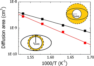
In order to give a quantitative discussion of the degree of anisotropy in the GaAs nanostructure, we plotted the diffusion area Dτ covered by the Ga atoms migration from the original droplet during As adsorption as a function of temperature, where D is the surface diffusion coefficient of Ga atoms and τ the time interval between arrival and adsorption of As atoms, that we can consider independent from the temperature, as discussed in Ref. [5]. To calculate the diffusion area for the two perpendicular crystallographic directions, we assumed a perfectly circular area with a radius given by each ring radius along [110] and [1–10] directions (r[110] and r[1–10] in the insets of Fig. 3). The difference between the obtained area and the inner ring area will give the desired diffusion area (yellow regions in the insets of Fig. 3), since the inner ring region is considered as the initial position of the Ga atoms before the As supply. The results are shown in Fig. 3 for both [110] (red squares) and [1–10] (black squares) directions, and the exponential dependence of Dτ on the temperature is confirmed in both cases. By the Arrhenius plot, the values of 1.28 and 0.85 eV for the activation energy for the Ga migration along [110] and [1–10], respectively, were obtained. We stress that these values are obtained by studying the surface migration of Ga in the case of the formation of our complex GaAs nanostructure constituted by concentric multiple rings. Since with our experimental procedure, the first structure to be formed is the outer one and the other rings are formed as a result of the Ga migration on a non perfectly flat GaAs (001) surface. In fact, the surface of the outer ring has a sub-nanometre surface roughness. Although it is not clear the detailed mechanism, the roughness of the actual surface over which gallium atoms can migrate might in general affect their diffusion length. Therefore, our experimental findings cannot be used to obtain the universal values for the activation energy of Ga atoms diffusion on GaAs (001) substrate. However, by means of these data, we can finely tune the diameter of each ring only by controlling the substrate temperature during the As supply. Operatively, this gives and important degree of freedom in the design of nanometre-size complex GaAs nanostructures. Since the electronic properties descend from the size and the shape of our materials, a good control over the dimension of the nanostructure is of the outmost relevance. Apart from the interest in the fundamentals of the crystal growth, these multiple rings systems can be used to investigate Aharonov–Bohm effect or serve as templates for the growth of ordered arrays of InAs quantum dots on GaAs. Each ring perimeter might be a preferential site for the nucleation of quantum dots, giving rise to circularly ordered arrays, as was already found in Ref. [11].
Figure 3.

Arrhenius plot of the diffusion area covered by Ga atoms during their migration from the Ga droplets as a function of the reverse temperature. In the insets: scheme of the procedure to calculate the diffusion area (yellow zone delimitated by the dashed line) for both [1–10] (top panel) and [110] (bottom panel). Solid lines represent the inner ring and an outer ring with a marked anisotropy
Conclusion
We have shown the fabrication method and the morphological analysis of GaAs concentric multiple rings structures grown in by DE. A five ring structure was created by exploiting the lateral growth of GaAs around the originally formed Ga droplets. Controlling the substrate temperature during the arsenic supply for the crystallization, it is possible to govern the diffusion length of Ga atoms and therefore each ring diameter. The nanostructures showed an anisotropy along [110] and [1–10] directions, and two different values of the activation energy for the diffusion of gallium atoms along these directions were obtained.
Misc
An erratum to this article can be found at http://dx.doi.org/10.1007/s11671-010-9816-6
Open Access
This article is distributed under the terms of the Creative Commons Attribution Noncommercial License which permits any noncommercial use, distribution, and reproduction in any medium, provided the original author(s) and source are credited.
References
- Koguchi N, Takahashi S, Chikyow T. J. Cryst. Growth. 1991. p. 688. COI number [1:CAS:528:DyaK3MXkvVamsro%3D]; Bibcode number [1991JCrGr.111..688K] [DOI]
- Koguchi N, Ishige K. Jpn. 1993. p. 2052. COI number [1:CAS:528:DyaK3sXks1Sjsb0%3D]; Bibcode number [1993JaJAP..32.2052K] [DOI]
- Watanabe K, Koguchi N, Gotoh Y. Jpn. 2000. p. L79. COI number [1:CAS:528:DC%2BD3cXhtlSqt7w%3D]; Bibcode number [2000JaJAP..39...79W] [DOI]
- Mano T, Koguchi N. J. Cryst. Growth. 2005. p. 108. COI number [1:CAS:528:DC%2BD2MXjsVelsro%3D]; Bibcode number [2005JCrGr.278..108M] [DOI]
- Somaschini C, Bietti S, Koguchi N, Sanguinetti S. Nano Lett. 2009. p. 3419. COI number [1:CAS:528:DC%2BD1MXhtFGlsLjE]; Bibcode number [2009NanoL...9.3419S] [DOI] [PubMed]
- Somaschini C, Bietti S, Sanguinetti S, Koguchi N, Fedorov A. Nanotechnology. 2010. p. 125601. COI number [1:STN:280:DC%2BC3c7lvVahuw%3D%3D]; Bibcode number [2010Nanot..21l5601S] [DOI] [PubMed]
- Aharonov Y, Bohm D. Phys. 1959. p. 485. Bibcode number [1959PhRv..115..485A] [DOI]
- Kleemans NAJM, Bominaar-Silkens IMA, Fomin VM, Gladilin VN, Granados D, Taboada AG, Garcia JM, Offermans P, Zeitler U, Christianen PCM, Maan JC, Devreese JT, Koenraad PM. Phys. 2007. p. 146808. COI number [1:STN:280:DC%2BD2sngslGisg%3D%3D]; Bibcode number [2007PhRvL..99n6808K] [DOI] [PubMed]
- Klimov VI, Mikhailovsky AA, Xu S, Malko A, Hollingsworth JA, Leatherdale CA, Eisler HJ, Bawendi MG. Science. 2000. p. 314. COI number [1:CAS:528:DC%2BD3cXnsVGisL0%3D]; Bibcode number [2000Sci...290..314K] [DOI] [PubMed]
- Imamoglu A, Awschalom DD, Burkard G, DiVincenzo DP, Loss D, Sherwin M, Small A. Phys. 1999. p. 4204. COI number [1:CAS:528:DyaK1MXnsVejtbo%3D]; Bibcode number [1999PhRvL..83.4204I] [DOI]
- Strom NW, Wang ZhM, Lee JH, AbuWaar ZY, Mazur YI, Salamo GJ. Nanoscale Res. 2007. p. 112. COI number [1:CAS:528:DC%2BD2sXktVart7k%3D]; Bibcode number [2007NRL.....2..112S] [DOI]


