Abstract
In this paper, we study the variation of the thickness of patterned microchannel features in photoresist (PR) by two-step photolithography. The final PR thickness is determined by the thickness and width of the predefined PR pattern in the first-step lithography and the thickness of the spin-coated PR film in the second-step lithography. Thickness variation is demonstrated to be an important consideration within the critical pattern width that the capillary pressure is still dominant for forming the PR film thickness. With this mechanism of two-step photolithography, we demonstrate its ability to form multilevel channel features and its use to fabricate a cross-flow filter with two different pore sizes as a microfluidic application.
INTRODUCTION
Photolithography is a process routinely used in fabrication of microdevices such as microfluidic devices, microelectronic circuits, and microelectromechanical systems by selectively removing parts of a thin photoresist (PR) film. The early microfluidic devices were fabricated in silicon, quartz, or glass through laborious processes such as chemical etching, reactive ion etching, and thermal bonding. The recent introduction of poly(dimethylsiloxane) (PDMS) for replica molding has revolutionized microfluidics by enabling simplified, faster prototyping with lower production cost and transferring multilevel, complex microfluidic patterns directly into the elastomer through replica molding.1, 2 Particularly, slant grooves or obstacles fabricated on a linear microchannel have been used for efficient mixing of solutions by using chaotic flows3, 4 and self-sorting of microbeads and mammalian cells by hydrophoresis.5, 6 A cross-flow filtration has been also implemented in microchannels with multiple heights, thereby achieving blood plasma separation and white blood cell enrichment.7, 8
There are several ways to fabricate master molds for multilevel microchannels, for instance, gray-scale photolithography,9 selective overexposure of a PR film to ultraviolet (UV) light,10 and microtunable elastomeric molds.11 Chen and co-workers9 described that the use of microfluidic photomasks that microchannels filled with a light-absorbing dye can produce microfluidic features of multiple heights by altering their opacity according to the dye concentration. Nock and Blaikie12 developed a similar gray-scale lithography technique with subwavelength patterned photomasks that were fabricated by electron beam lithography and reactive ion etching. Toepke and Kenis10 showed that selective overexposure of a PR film to UV light can pattern it with features of different heights by using a photomask with masking lines of different widths. Hoffman et al.11 developed tunable elastomeric molds consisting of a thin PDMS membrane with sealed cavities that can be pressurized and form microfluidic features of different heights. Although these methods have been successfully demonstrated in a single lithography step, they have some disadvantages such as requirement of costly photomasks or difficulty about wafer-level batch production.
Multistep lithography is one of the simplest ways to fabricate microfluidic features of different heights. Although there is an alignment issue for the fabrication process, it is a routine work that a wafer will go through the lithographic cycle up to several tens of times in fabrication of integrated microelectronic circuits. Many researchers have been studied for formation of a thin liquid film over uneven topography in the aspect of rheology and dynamics of the film formation on microelectronic circuits.13, 14, 15, 16 Herein we provide the detailed understanding of two-step photolithography for microfluidic applications and its use to fabricate multilevel microchannels and a cross-flow filter with two different pore sizes as a microfluidic application.
MATERIALS AND METHOD
Two-step lithography
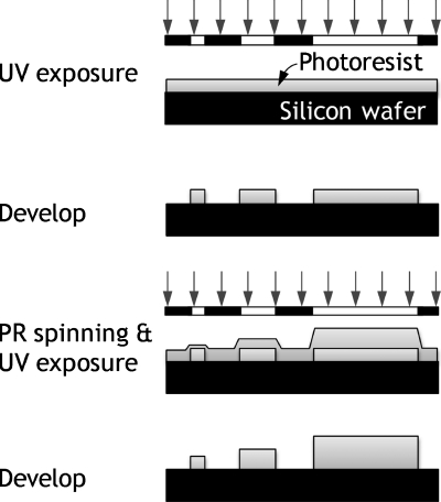
The PR mold for multilevel microchannels was defined on a silicon wafer using two-step photolithography (Fig. 1). The first spin-coating of an UV-curable PR (SU8-2005 or SU8-2010, MicroChem Corp., MA) defined linear features that have different widths ranging from 20 to 600 μm with 200 μm spacing. In the second-step lithography, the PR (SU8-2010 or SU8-2025, MicroChem Corp.) was spin-coated on the previously patterned PR mold and then exposed to UV light through the second photomask that was aligned with respect to the previously developed SU8 patterns. We measured the height of the fabricated microfluidic features using a surface profiler (Alpha-Step 500, KLA-Tencor Corp., CA). For replica molding, the PDMS mixture of PDMS and its curing agent (the ratio of 10:1) was poured on the PR mold and cured for 3 h in a convection oven at 65 °C for complete cross-linking. To seal the microchannels, we bonded a PDMS layer and a glass slide to each other after brief exposure of oxygen plasma for 30 s.
Figure 1.
Schematic drawing of two-step lithography process to fabricate multilevel microchannels.
Sample preparation
Fluorescent polystyrene beads with a diameter of 2 μm (Polysciences, Warrington, PA) and nondyed polystyrene beads with a diameter of 6 μm (Polysciences) and 15 μm (Molecular Probes, Eugene, OR) were used to demonstrate the usefulness of the fabricated multilevel microchannel by filtering the beads. The beads were prepared in 2% Pluronic F68 solution (Sigma-Aldrich, St. Louis, MO) with an average concentration of1.3×103, 3.4×10², and50 particles∕μl, respectively.
Experimental setup
The microchannels were imaged with an inverted microscope (TS100, Nikon Co., Japan) equipped with a charge-coupled device (DS-2 MBWc, Nikon Co.). A syringe pump (Pump 11 Pico Plus, Harvard Apparatus, MA) was used to produce a 1 μl∕min flow through the microchannels.
RESULTS AND DISCUSSION
Figure 1 shows a schematic of the two-step lithography process used to pattern the PR with microfluidic features of different heights. During the spin costing of PR over a flat substrate (e.g., the first-step lithography), the centrifugal force that drives PR flow is balanced with the viscous force that resists PR flow, thereby forming a uniform film. During the spin-coating over an uneven substrate (e.g., the second-step lithography), the capillary force begins to act on a PR film and will tend to drive the fluid into the substrate, thus reducing the curvature of the film surface over predefined PR patterns and lowering the film thickness. The capillary pressure Pcap generated by the capillary force is proportional to the interfacial tension γ and inversely proportional to the radius of curvature of the air-film interface R (Fig. 2). Whenhf⪢h−hs, w⪢hf, and assuming that the film surface over the predefined PR pattern is in semispherical shape, the capillary pressure is given by13
| (1) |
where hf and w are the height and width of the defined PR pattern in the first-step lithography, respectively, hsis the thickness of the spin-coated PR film on the wafer surface in the second-step lithography, and h is the thickness of the PR film deposited right on the predefined PR pattern. The capillary pressure gradient ∇Pcap acting over the PR pattern is estimated by dividing pcap byw∕2,
| (2) |
The capillary pressure acting on a PR film over a predefined PR pattern increases in a cubic-power manner as the pattern width decreases, thereby lowering the film thickness. Therefore, the two-step lithography process allows to control the height of the final PR patterns by making small adjustments in the width of PR patterns defined for the first-step lithography.
Figure 2.
Schematic of the PR film profile over a rectangular PR pattern when the centrifugal and capillary forces are balanced.
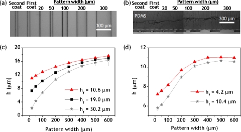
We demonstrated the ability to fabricate multilevel microfluidic features in a single mold by making small adjustments in the width of PR pattern defined in the first-step lithography using two-step lithography process. A 30.2-μm -thick layer of SU8 was deposited and patterned on a silicon wafer to create a master with features of varying widths that eventually create varying heights. The SU8 patterns were formed with a series of linear lines ranging from 20 to 600 μm in widths separated by 200 μm spacing. A 20.1-μm -thick layer of SU8 was deposited again on the master and then exposed to UV light through the second photomask that was aligned with respect to the previously developed SU8 patterns. Figures 3a, 3b show PDMS replicas made from the photoresist master in top view and cross-sectional view, respectively. The change in replica feature height relative to PR pattern width results from the intensity of capillary pressure acting on the two sides of uneven topography as mentioned before. The feature heights of PR masters and corresponding coating thicknesses we measured are provided in Figs. 3c, 3d. The capillary pressure acting on a PR film over a predefined PR pattern increases in a cubic-power manner as the pattern width decreases, and linearly increases as the thickness of the PR pattern increases. Since the capillary pressure works for lowering the film thickness, the final feature height of PR masters is determined by the pattern width and the coating thickness in the first-step lithography. This dependence of the capillary pressure on topography allows to control the height of the final PR patterns by making small adjustments in the width of PR pattern defined in the first-step lithography.
Figure 3.
Thickness variation of patterned microchannel features fabricated by two-step photolithography. (a) Optical top-view image of multilevel microchannels molded in PDMS. The first and second coats refer to the first and second PR coating layers, respectively. The layer thicknesses were hf=30.2 μm andhs=20.1 μm. (b) Optical cross-sectional image of the microchannels. (c) Measurements of h vs pattern width. The second layer thickness hs for all cases was fixed at 20.1 μm on average, while the first layer thickness varied from 10.6 to30.2 μm. (d) Measurements of h vs pattern width. The second layer thickness hs for all cases was fixed at 10.8 μm on average, while the first layer thickness varied from 4.2 to10.4 μm.
The capillary force acting on a PR film over a predefined PR pattern decays as the pattern width increases and is finally overwhelmed by the centrifugal force. The critical pattern width wc that the capillary pressure is still dominant for forming the PR film thickness can be calculated by balancing with the centrifugal pressure. The centrifugal pressure gradient ∇Pcent generated from the centrifugal force is given by
| (3) |
where ρ is the density of the PR, ωis the angular velocity, and r is the radial position. The critical pattern width that the centrifugal pressure gradient is equal to the capillary pressure gradient is given by13
| (4) |
Assumingγ, hf, ρ, ω, and r of 40.4 dyn∕cm, 20 μm, 1 g∕cm3, 210 rad∕s (2000 rpm), and 3 cm, respectively, we obtain a value of approximately 210 μm forwc. Thus, the height of the PR masters is rapidly varied in the width range from 20 to 210 μm within the critical pattern width.
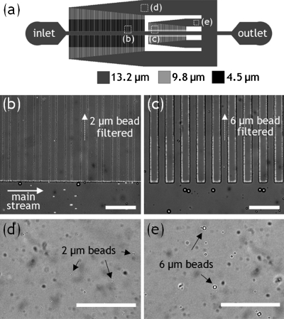
In order to demonstrate the utility of the method for fabrication of multilevel microchannels, we fabricated a cross-flow filter with three different heights (Fig. 4). The SU8 patterns of the side-channels for sorting 2 μm beads were formed in a thickness of 4.5 μm with a series of linear lines of 20 μm in width. A 9.8-μm -thick layer of SU8 was deposited again and formed the side-channels of 20 μm in width for sorting 6 μm beads. The combination of the depositions finally forms the main channel in a thickness of≈13.2 μm. A bead mixture containing 2, 6, and 15 μm beads was injected into the filter at a flow rate of1 μl∕min. With this filter, we can successfully perform the cross-flow filtration by sorting 2, 6, and 15 μm beads, as shown in Figs. 4b, 4c. The 2 μm beads smaller than the 4.5-μm -high side-channels passed through the side-channels, while 4 and 15 μm beads were all retained in the main channel [Fig. 4d]. The 6 μm beads smaller than the 9.8-μm -high side-channels, although still mixed with 2 μm beads, passed through the side-channels, while 15 μm beads were all retained in the main channel [Fig. 4e]. The separation selectivity of the 6 μm beads is affected by the majority of 2 μm beads that are still retained in the main channel. The separation selectivity of the 6 μm beads could be further enhanced by employing a perfusion flow to push all the 2 μm beads into the 4.5-μm -high side-channels.8 Although we demonstrated a simple cross-flow filter with two different pore sizes, its side-channel thickness can be further varied by the aforementioned mechanism of two-step photolithography, thereby improving the separation capability of the cross-flow filter. In this case, the side-channel thickness can be rapidly varied in the width range from 20 to 130 μm within the critical pattern width of130 μm. In addition, this fabrication method can be exploited in other microfluidic applications that require multilevel microchannels such as cell trapping,17 micromixer,3, 4 and cell separation.5, 6, 7, 8
Figure 4.
Microfluidic cross-flow filter fabricated by two-step photolithography. (a) Schematic of a cross-flow microfluidic filter with three different channel heights of 4.5, 9.8, and13.2 μm. (b) 2 μm beads entering 4.5-μm -high side-channels from the main channel, sorted from 6 and 15 μm beads. A fluorescence image of 2 μm beads was superimposed on a bright field image. (c) 2 and 6 μm beads entering 9.8-μm -high side-channels from the main channel, sorted from 15 μm beads. (d) 2 μm beads after passing through the 4.5-μm -high side-channels. (e) 2 and 6 μm beads after passing through 9.8-μm -high side-channels. All scale bars are100 μm.
CONCLUSION
This paper provides the detailed mechanism of two-step photolithography for microfluidic applications and shows how to use the mechanism for fabrication of multilevel microchannels. The final PR thickness in two-step lithography is determined by the thickness and width of the defined PR pattern in the first-step lithography and the thickness of the spin-coated PR film in the second-step lithography. The critical pattern width wc provides a simple means to assess the thickness control range. This simple mechanism allows fabrication of multilevel channels applicable to microfluidic applications such as cell trapping, micromixer, and cell separation.
ACKNOWLEDGMENTS
This research was supported by the National Research Laboratory (NRL) Program (Grant No. R0A-2008-000-20109-0), the Nano∕Bio Science and Technology Program (Grant No. 2008-00771), and the Converging Research Center Program (Grant No. 2009-0093663) through the National Research Foundation of Korea funded by the Ministry of Education, Science and Technology (MEST).
References
- Duffy D. C., McDonald J. C., Schueller O. J. A., and Whitesides G. M., Anal. Chem. 70, 4974 (1998). 10.1021/ac980656z [DOI] [PubMed] [Google Scholar]
- Friend J. and Yeo L., Biomicrofluidics 4, 026502 (2010). 10.1063/1.3259624 [DOI] [PMC free article] [PubMed] [Google Scholar]
- Stroock A. D., Dertinger S. K. W., Ajdari A., Mezić I., Stone H. A., and Whitesides G. M., Science 295, 647 (2002). 10.1126/science.1066238 [DOI] [PubMed] [Google Scholar]
- Du Y., Zhang Z., Yim C., Lin M., and Cao X., Biomicrofluidics 4, 024105 (2010). 10.1063/1.3427240 [DOI] [PMC free article] [PubMed] [Google Scholar]
- Choi S. and Park J. -K., Lab Chip 9, 1962 (2009). 10.1039/b820364d [DOI] [PubMed] [Google Scholar]
- Choi S., Song S., Choi C., and Park J. -K., Anal. Chem. 81, 1964 (2009). 10.1021/ac8024575 [DOI] [PubMed] [Google Scholar]
- VanDelinder V. and Groisman A., Anal. Chem. 78, 3765 (2006). 10.1021/ac060042r [DOI] [PubMed] [Google Scholar]
- VanDelinder V. and Groisman A., Anal. Chem. 79, 2023 (2007). 10.1021/ac061659b [DOI] [PubMed] [Google Scholar]
- Chen C., Hirdes D., and Folch A., Proc. Natl. Acad. Sci. U.S.A. 100, 1499 (2003). 10.1073/pnas.0435755100 [DOI] [PMC free article] [PubMed] [Google Scholar]
- Toepke M. W. and Kenis J. A., J. Am. Chem. Soc. 127, 7674 (2005). 10.1021/ja050660+ [DOI] [PubMed] [Google Scholar]
- Hoffman J. M., Shao J., Hsu C. -H., and Folch A., Adv. Mater. (Weinheim, Ger.) 16, 2201 (2004). 10.1002/adma.200400441 [DOI] [Google Scholar]
- Nock V. and Blaikie R. J., Microelectron. Eng. 85, 1077 (2008). 10.1016/j.mee.2008.01.088 [DOI] [Google Scholar]
- Stillwagon L. E., Larson R. G., and Taylor G. N., J. Electrochem. Soc. 134, 2030 (1987). 10.1149/1.2100813 [DOI] [Google Scholar]
- Kalliadasis S., Bielarz C., and Homsy G. M., Phys. Fluids 12, 1889 (2000). 10.1063/1.870438 [DOI] [Google Scholar]
- Peurrung L. M. and Graves D. B., J. Electrochem. Soc. 138, 2115 (1991). 10.1149/1.2085935 [DOI] [Google Scholar]
- Mazouchi A. and Homsy G. M., Phys. Fluids 13, 2751 (2001). 10.1063/1.1401812 [DOI] [Google Scholar]
- Di Carlo D., Aghdam N., and Lee L. P., Anal. Chem. 78, 4925 (2006). 10.1021/ac060541s [DOI] [PubMed] [Google Scholar]


