Abstract
We demonstrate lensfree on-chip sensing within a microfluidic channel using plasmonic nanoapertures that are illuminated by a partially coherent quasimonochromatic source. In this approach, lensfree diffraction patterns of metallic nanoapertures located at the bottom of a microfluidic channel are recorded using an optoelectronic sensor-array. These lensfree diffraction patterns can then be rapidly processed, using phase recovery techniques, to back propagate the optical fields to an arbitrary depth, creating digitally focused complex transmission patterns. Cross correlation of these patterns enables lensfree on-chip sensing of the local refractive index surrounding the near-field of the plasmonic nanoapertures. Based on this principle, we experimentally demonstrate lensfree sensing of refractive index changes as small as ∼2×10⁻³. This on-chip sensing approach could be quite useful for development of label-free microarray technologies by multiplexing thousands of plasmonic structures on the same microfluidic chip, which can significantly increase the throughput of sensing.
Metallic apertures support surface plasmon waves that are localized to the near-field of the aperture structure. Physical properties of these plasmonic waves, by their nature, are rather sensitive to the local refractive index of the medium surrounding the aperture region. As the size of the metallic aperture goes subwavelength, direct transmission of light through the aperture becomes extremely inefficient and the transmission behavior of these apertures starts to be dominated by plasmonic effects, exhibiting strong sensitivity to the refractive index of the surrounding medium as well as to the wavelength, polarization, and the angle of the illumination light.1, 2 Nanoscale features of these metallic apertures also help coupling of free space radiation into surface plasmon waves, which can then also couple out to propagating transmission waves, enabling far-field sensing of the near-field effects occurring at the aperture region. These unique properties of plasmonic nanostructures have already been utilized to create various optical sensor architectures.3, 4, 5, 6, 7, 8
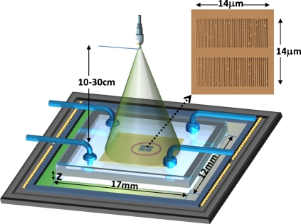
To provide a complementary effort, here we introduce an alternative technique to use metallic nanoapertures as optical sensing elements on a chip. In our approach, different than the prior art, lensfree diffraction patterns of plasmonic nanoaperture arrays located on a microfluidic chip are utilized for sensing. For this purpose, we use spatially incoherent quasimonochromatic illumination, which picks up partial spatial coherence during its propagation that is sufficiently large to coherently illuminate each nanostructured aperture region (e.g., 14×14 μm2, see Fig. 1). Under this illumination condition, the coherent diffraction pattern of each nanoaperture region can be sampled using an optoelectronic sensor array such as a complementary metal-oxide-semiconductor (CMOS) chip. This lensfree pattern can then be digitally processed to rapidly retrieve the missing phase of the optical diffraction, enabling back-propagation of the fields to an arbitrary depth below the nano-aperture plane.9, 10 If the plasmonic apertures are designed appropriately, these lensfree diffraction patterns reconfigure their transmission behavior in response to the local refractive index surrounding the near-field of the apertures. Therefore by performing cross correlation among these reconstructed diffraction patterns, lensfree on-chip sensing of minute local refractive index changes would be feasible.
Figure 1.
Lensfree on-chip sensing setup. A plasmonic nanoaperture array, as shown in the SEM image on the top right corner, is illuminated with a quasimonochromatic source (e.g., 550 nm center wavelength with ∼20 nm bandwidth) located ∼10–30 cm away from its surface. The lensfree transmission pattern of this plasmonic structure is sampled by a CMOS chip placed at z∼1 mm away from the aperture plane. The yellow surface indicates the detector active area (∼6×4 mm2). The plasmonic nanoaperture array shown above is composed of uniformly spaced slits each with a length of ∼6 μm where the slit width varied (from left to right) between ∼80 and ∼200 nm in discrete steps of ∼20 nm. The physical gap between two neighboring slits is kept constant at ∼200 nm.
A major advantage of this lensfree on-chip sensing platform over existing approaches is that it has significantly increased throughput since the entire active area of the optoelectronic detector (e.g., a CMOS chip) can now be utilized with unit magnification (see Fig. 1). This makes it feasible to multiplex literally thousands of plasmonic aperture arrays on a standard CMOS chip with an active detector area of, e.g., >20–100 mm2, which could especially create important opportunities for designing label-free DNA or protein micro-arrays. Furthermore, lensfree on-chip architecture of this platform also makes it rather compact and light-weight which are important features for practical implementations of the same platform for point-of-care and field use, aiming, e.g., various global health challenges including water quality screening and diagnosis of infectious diseases. It is particularly important to note the compatibility of this on-chip plasmonic sensing approach with the recently demonstrated lensfree telemedicine microscopes10, 11 such that a complete solution (involving both lensfree microscopy and on-chip sensing) can be put together within the same field-portable telemedicine unit. This could potentially create better opportunities for health-care delivery in resource poor settings.
To implement the above discussed lensfree on-chip sensing architecture, we chose to work with a plasmonic aperture array design12 that is composed of varying widths of rectangular subwavelength apertures∕slits spanning an area of ∼14×14 μm2 as illustrated in Fig. 1. A similar nanoaperture array has been previously utilized to design planar lenses by exploiting the linear relationship between the width of the subwavelength slit and the phase of the transmitted optical field.12 In our on-chip sensing implementation, however, the function of this array of subwavelength slits with varying widths was to introduce different diffraction patterns as a function of the local refractive index. This plasmonic structure (see Fig. 1) was fabricated using focused ion-beam milling (NOVA 600) on borosilicate cover slips (150 μm thick) that were coated with ∼200 nm gold layer using electron beam metal deposition (CHA Mark40, UCLA Nanolab). The prepared chip was then used as the bottom substrate of a custom designed microfluidic device as illustrated in Fig. 1. The liquid samples having different refractive indices were flushed into the microfluidic chamber to interact with the near-field of the nanoapertures by means of an automated syringe pump. Lensfree diffraction patterns corresponding to each refractive index value were continuously captured on a chip at a frame rate of ∼2–3 fps using a CMOS image sensor while the liquid was flowing through the microfluidic channel (see Fig. 1). The illumination was achieved using a monochromator at 550 nm with a spectral bandwidth of ∼20 nm, which indicates that a standard light-emitting diode could also be used in terms of both spatial and temporal coherence properties. We have also used an inexpensive plastic polarizer in front of the illumination source to create a linear polarization that is orthogonal to the slit direction. This ensured that the transmitted fields from the plasmonic nanoapertures contained only a single polarization component, which is important for phase recovery steps, as will be outlined later on. This was also confirmed through finite-difference time-domain (FDTD) simulations.
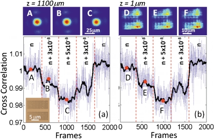
To experimentally validate the sensitivity of this lensfree platform, we used salt-water with well-controlled concentrations such that the exact value of the liquid refractive index could be extracted from a look-up table.13 Figures 2a, 2b, 2c top-left images illustrate the lensfree diffraction patterns of our nanoaperture array (sampled at z=1100 μm as shown in Fig. 1) for three different refractive index values, n=1.333 [corresponding to de-ionized (DI) water], n+3×10⁻³, and n+5×10⁻³, respectively. To better quantify the numerical differences among these lensfree diffraction patterns and relate them to refractive index changes (Δn) within the microchannel, we calculated 2D cross correlation coefficients between the first lensfree pattern (corresponding to DI water) and the rest of the acquired diffraction images. Figure 2a left-bottom plot illustrates the results of this cross correlation calculations with a dotted blue curve for ∼2000 consecutive lensfree diffraction patterns, which were captured while the refractive index within the microchannel was changed according to the following discrete steps: (1)n=1.333,(2)n+3×10⁻³,(3)n+5×10⁻³, (4)n+3×10⁻³, (5)n=1.333.
Figure 2.
Cross correlation coefficients are calculated between the first lensfree transmission pattern and the subsequent patterns for (a) the detector plane (z=1100 μm) and (b) z=1 μm reconstruction plane, as illustrated with the blue dotted lines. The same plots also show the running averages of these cross correlation coefficients over ∼50 frames as shown with the black solid lines in (a) and (b). The intensities of the lensfree transmission patterns used in (a) and (b) are normalized to the instantaneous illumination intensity, which is also detected using the same CMOS chip through a large aperture. The initial refractive index of these sensing experiments (n) is 1.333 corresponding to DI water. Top row: (a)–(c) illustrate the raw lensfree diffraction patterns of the nanoaperture array at three different refractive indices within the microfluidic channel (n, n+3×10⁻³, and n+5×10⁻³, respectively), where all the lensfree transmission patterns extend over a width of >50 μm. Top row (d)–(f) illustrate the reconstructed transmission patterns of the same nanoaperture array at z=∼1 μm plane, right underneath the aperture region.
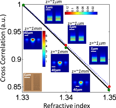
The solid black curve in the same Fig. 2a also illustrates a running average of the cross correlation coefficients for a window size of ∼50 frames. As illustrated in these results, by recording the lensfree diffraction patterns of this plasmonic aperture array on a compact chip we can faithfully track refractive changes as small as Δn=2×10⁻³. To further validate our results, we have also performed FDTD simulations of the same plasmonic structure, the results of which are summarized in Fig. 3. According to these FDTD simulations, the far-field lensfree diffraction patterns of our nanoaperture array closely match our experimental results presented in Figs. 2a, 2b, 2c. Furthermore, the same FDTD results also indicate that, as desired, the response of the 2D cross correlation coefficient of these lensfree diffraction patterns is linear over a large refractive index range spanning 1.33–1.35.
Figure 3.
Based on FDTD simulation results, the cross correlation coefficients among lensfree transmission patterns of the same nanoaperture array shown in Figs. 12 are calculated as a function of the refractive index within the microchannel. These calculations were performed for both z=∼1 mm (solid line) and z=∼1 μm (dashed line) planes. False color insets depict the 2D transmission patterns for three different refractive index values (1.33, 1.34, and 1.35, respectively), where the upper (lower) ones are calculated at z=∼1 μm (z=∼1 mm).
While these experimental and FDTD simulation results both demonstrate the useful sensitivity of the proposed lensfree on-chip sensing scheme, there is still room for further improvement that can be implemented by utilizing more advanced digital processing of these diffraction patterns. In particular, due to its lensfree operation, the sampled transmission patterns of the plasmonic aperture array spread over a large area on the sensor chip. While this has no negative consequences for a low number of spots on the same chip, it would create significant limitations as one aims to increase the density and hence the throughput of sensing. In other words, as more and more independent plasmonic spots are placed on the same chip (e.g., toward a label-free DNA or protein microarray design), their lensfree diffraction patterns will overlap with each other at the detector, which would degrade the sensitivity of the lensfree sensing platform.
To mitigate this challenge and increase the density of the sensing spots on the same microfluidic chip, we have used an iterative phase recovery technique9, 10, 11 to reconstruct the complex wave corresponding to the transmission pattern of each nanoaperture array. In this numerical approach, we treat the detected lensless pattern as the intensity of a complex optical wave whose phase was lost during the image acquisition. To recover this lost phase, we start with an arbitrary phase distribution at the detector plane and back propagate this complex wave to the plasmonic aperture plane.10 Since the physical boundaries of the aperture region (e.g., ∼14×14 μm2 in Fig. 1) is known a priori, we can enforce this size information as a spatial filter for the complex fields at the aperture plane and forward propagate the filtered fields back to the detector plane, where the optical phase will now change to a 2D function. By replacing the intensity at the detector plane with the measured one, and keeping the updated phase distribution, we can start the next iteration to better estimate the phase of the diffracted field after each cycle. This iterative approach rapidly converges to a unique solution after typically 10–15 iterations which take <1 s using a standard graphics processing unit.10
To illustrate its performance, in Figs. 2d, 2e, 2f we demonstrate the iterative reconstruction results of the field intensity at the plasmonic aperture plane using the raw lensfree diffraction patterns shown in Figs. 2a, 2b, 2c. If we now calculate the 2D cross correlation coefficients among these reconstructed patterns, we can get an updated sensing curve as illustrated in Fig. 2b, bottom-right plot. Once again, similar to Fig. 2a, we can faithfully track refractive changes as small as Δn=2×10⁻³, this time using the reconstructed optical intensity patterns at the aperture plane. The major advantage of this phase recovery based approach is that it would enable multiplexing more densely packed plasmonic spots such that the overall throughout of on-chip sensing can be significantly increased without affecting the sensitivity of the platform. We have also conducted FDTD simulations to calculate the field patterns close to the aperture plane, the results of which are summarized in Fig. 3, nicely matching to our experimental results shown in Fig. 2.
It is rather important to emphasize that the above discussed iterative phase recovery approach works even if the diffraction patterns of neighboring plasmonic spots overlap at the detector plane, see e.g., Figs. 2d, 2e, 2f, where the transmission patterns of the top and bottom aperture arrays are resolved from each other, which normally were entirely overlapping at the detector plane as shown in Figs. 2a, 2b, 2c. In addition to this, as the sensing field of view increases to cover the entire detector active area (e.g., >20 mm2), the requirements for spatial and temporal coherence of illumination would not change, which is quite important for scaling this platform to extreme throughputs without changing the illumination conditions. In this sense, the operation principles of this phase recovery approach is quite similar (although not identical) to recently demonstrated partially coherent lensfree holographic telemedicine microscopes,10, 11 where the lensfree cell holograms over a large field of view cannot coherently interfere with each other due to the limited spatial coherence diameter at the detector plane. The exact value of the spatial coherence diameter in our lensfree platform can be precisely be tuned by controlling the aperture size of the source or by controlling the propagation distance between the source and the plasmonic aperture planes.
We should finally note that fabrication imperfections of the plasmonic nanostructures in our design do not constitute a fundamental challenge in our lensfree on-chip sensing approach, since we are effectively measuring the cross correlation variations of the lensfree diffraction patterns of the plasmonic apertures as function of the local refractive index. This differential correlation measurement makes our scheme robust to potential fabrication imperfections, which is especially important for wide field of view implementations of this platform for increased throughput in sensing.
Acknowledgments
A. Ozcan acknowledges the support of NSF (CAREER Award on BioPhotonics Program), (ONR) Young Investigator Award and the NIH Director’s New Innovator Award No. DP2OD00642 .
References
- Genet C. and Ebbesen T. W., Nature (London) 445, 39 (2007). 10.1038/nature05350 [DOI] [PubMed] [Google Scholar]
- García-Vidal F. J., Martín-Moreno L., Moreno E., Kumar L. K. S., and Gordon R., Phys. Rev. B 74, 153411 (2006). 10.1103/PhysRevB.74.153411 [DOI] [Google Scholar]
- Cooper M. A., Nat. Rev. Drug Discovery 1, 515 (2002). 10.1038/nrd838 [DOI] [PubMed] [Google Scholar]
- Stewart M. E., Anderton C. R., Thompson L. B., Maria J., Gray S. K., Rogers J. A., and Nuzzo R. G., Chem. Rev. 108, 494 (2008). 10.1021/cr068126n [DOI] [PubMed] [Google Scholar]
- Sannomiya T., Balmer T. E., Hafner C., Heuberger M., and Vörös J., Rev. Sci. Instrum. 81, 053102 (2010). 10.1063/1.3405912 [DOI] [PubMed] [Google Scholar]
- Lee K. L., Lee C. W., Wang W. S., and Wei P. K., J. Biomed. Opt. 12, 044023 (2007). 10.1117/1.2772296 [DOI] [PubMed] [Google Scholar]
- Canpean V. and Astilean S., Lab Chip 9, 3574 (2009). 10.1039/b914235e [DOI] [PubMed] [Google Scholar]
- Liedberg B., Nylander C., and Lunström I., Sens. Actuators 4, 299 (1983). 10.1016/0250-6874(83)85036-7 [DOI] [Google Scholar]
- Oh C., Isikman S. O., Khademhosseinieh B., and Ozcan A., Opt. Express 18, 4717 (2010). 10.1364/OE.18.004717 [DOI] [PMC free article] [PubMed] [Google Scholar]
- Mudanyali O., Tseng D., Oh C., Isikman S. O., Sencan I., Bishara W., Oztoprak C., Seo S., Khademhosseinieh B., and Ozcan A., Lab Chip 10, 1417 (2010). 10.1039/c000453g [DOI] [PMC free article] [PubMed] [Google Scholar]
- Tseng D., Mudanyali O., Oztoprak C., Isikman S. O., Sencan I., Yaglidere O., and Ozcan A., Lab Chip 10, 1787 (2010). 10.1039/c003477k [DOI] [PMC free article] [PubMed] [Google Scholar]
- Verslegers L., Catrysse P. B., Yu Z., White J. S., Barnard E. S., Brongersma M. L., and Fan S., Nano Lett. 9, 235 (2009). 10.1021/nl802830y [DOI] [PubMed] [Google Scholar]
- Lide D. R., Handbook of Chemistry and Physics (CRC-LCC, Bacon Raton, FL, 2004). [Google Scholar]


