Abstract
We present a monolithic, solidly-mounted CMOS-FBAR oscillator array for mass sensing applications. Thin-film bulk acoustic resonators (FBAR) are an effective platform for sensitive biological and chemical detection, where their high operating frequencies make them many times more sensitive than a quartz crystal microbalance. By monolithic integration with CMOS drive circuitry, we aim to overcome the spatial limitations of externally-coupled resonators to build dense sensor arrays without specialized fabrication techniques. The sensors in this work are constructed in a 6 × 4 array atop a 0.18μm CMOS active substrate, and mass sensitivity comparable to off-chip FBAR sensors is demonstrated.
Keywords: FBAR, mass sensor, bioelectronics, CMOS
INTRODUCTION
Ultra-high-precision mass sensing is an important emerging detection method for biomolecular and chemical detection. Detecting molecules by mass requires no chemical or fluorescent labeling, allowing for simplified detection protocols and for sensing in systems adversely affected by labeling. Mass sensing is best performed by monitoring the resonant frequency of a lightweight, high-Q mechanical resonator that is in contact with the material to be measured. An increase in mass at the resonator surface causes an overall decrease in the resonant frequency of the loaded system, and this frequency can be measured and used to determine the mass addition [1].
The high resonant frequencies achievable in thin-film bulk acoustic resonators (FBARs) allow for sensitivities >1000× those of other resonant structures such as quartz crystal microbalances (QCM)[1]. FBAR resonators have also found use in microwave circuit applications, where sharp resonances at high frequency make them ideal for use in filters and oscillators [2,3]. These structures are typically interfaced with active CMOS components through wire-bonding [2,3] or flip-chip [4] connection approaches, which prevent more than one or two resonators from being integrated with a single chip. Others have implemented membrane BAW structures directly on CMOS for microwave applications [5].
In this work, we present the first monolithic solidly-mounted CMOS-FBAR oscillator array for mass sensing applications. In contrast to externally coupled FBAR structures, this approach allows for implementation of an integrated array of sensors built directly above its drive and readout circuitry. An array of mass sensors, each functionalized for capturing a specific protein, DNA, or gas molecule will allow simultaneous, multiplexed, high-sensitivity measurement of multiple targets on a single sensor chip.
FBAR MASS SENSOR
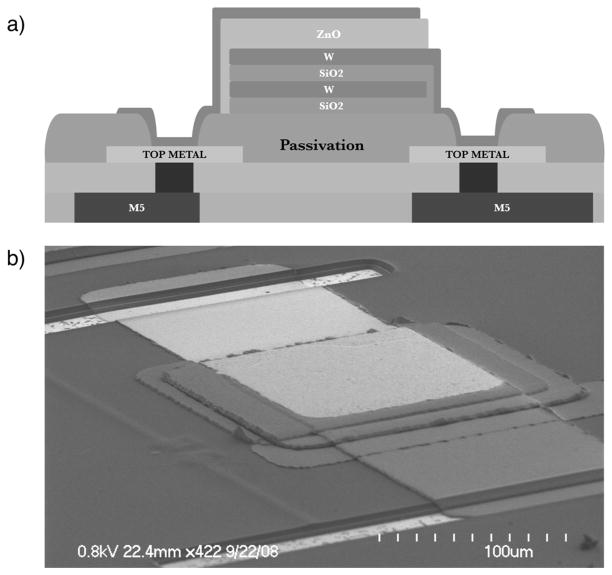
The solidly-mounted FBAR sensor comprises a piezoelectric zinc oxide resonator atop a mechanically isolating acoustic mirror [6]. The mirror functions as a mechanical analog to the optical Bragg stack, as acoustic waves are reflected back into the resonator through quarter-wavelength layers and constructive interference. This structure allows for simple fabrication, as depicted schematically in Figure 1a. The sensor is built up via sequential deposition and patterning of each layer and requires no undercutting or sacrificial layer integration processes. This can be accomplished on a passive substrate, or, as is shown in Figure 1b, monolithically atop an active CMOS substrate.
Figure 1.
The solidly mounted FBAR comprises an acoustic c zinc oxide layer on a CMOS mirror (W/SiO2) and a piezoelectri integrated circuit substrate, shown both (a) schematically and (b) realized and imaged via SEM micrograph.
FBAR-CMOS OSCILLATOR
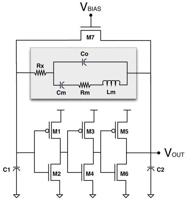
The FBAR resonator can be connected to an inverting CMOS amplifier to form an integrated FBAR-CMOS oscillator. The oscillator circuit in this implementation follows a standard Pierce oscillator topology, shown in Figure 2. The inverting amplifier is implemented as three in-line CMOS inverters formed by M1-M6, which ensures sufficient gain to overcome the FBAR material losses to sustain oscillation. M7 serves to bias M1-M6, and its gate voltage can be externally controlled to balance biasing strength with oscillator loading; this accommodates inherent variations in FBAR design and fabrication. C1 and C2 are formed by MIM capacitors set to equal values to promote oscillator startup. The FBAR, whose equivalent Butterworth-Van Dyke circuit model is depicted in the grey box, serves as a high-Q resonant tank for the oscillator [6].
Figure 2.
A single sensor of the global 6×4 FBAR-CMOS array architecture displays the Pierce oscillator topology. The FBAR equivalent circuit model is shown in the grey box, with Cm, Rm, and Lm corresponding to the motional components and Co, Rx corresponding to the intrinsic electrical properties of the zinc oxide structure.
CMOS POST-FABRICATION
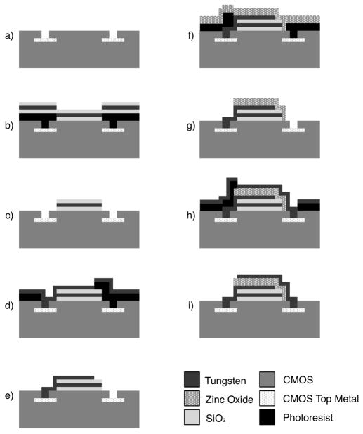
FBARs are built atop the CMOS microchip using the process flow illustrated in Figure 3. We first construct the acoustic mirror by RF sputtering alternating layers of silicon dioxide (750nm) and tungsten (650nm) onto a patterned CMOS substrate, which has been fabricated using a commercial 0.18μm foundry CMOS process. The top tungsten mirror layer also serves as the bottom electrode of the FBAR, and this layer also connects to the top metal layer of the CMOS substrate through an opening in the passivation layer. The zinc oxide layer (1450nm) is RF sputtered, and its crystallographic orientation (<002>) is confirmed through a sharp 34.4° peak in the 2θ X-ray diffraction pattern. Finally, a top tungsten contact (200nm) is patterned and connects through CMOS top metal to the underlying oscillator circuitry.
Figure 3.
CMOS post-fabrication of FBAR sensors is shown schematically: a bare CMOS die showing access to top metal through cuts in passivation (a) is subject to patterning, deposition, and lift-off of tungsten/silicon-dioxide acoustic mirror (b,c), tungsten FBAR bottom contact (d,e), piezoelectric zinc oxide (f,g), and tungsten FBAR top contact (h,i).
INTEGRATED SENSOR ARRAY
FBAR structures are built atop individual CMOS dice in a regular 6 × 4 array as shown in the die photo of Figure 4, and control circuitry and sensor test sites are also outlined. The test sites provide for standalone testing of active FBAR-CMOS oscillators and of a passive FBAR resonator. Each array oscillator occupies 0.13 mm2, and array density is limited primarily by the area of the FBAR sensors rather than by the area of the underlying circuits. As tested, each resonator comprises a 100μm × 100μm square structure, as defined by the overlap of top and bottom tungsten contacts. Optimization of the FBAR size will lead to smaller FBAR footprints and a higher array density in future implementations.
Figure 4.
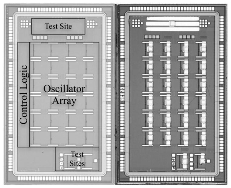
Left die photo shows CMOS as returned from foundry. Boxes indicate layout of underlying CMOS architecture. Right die photo shows chip after fabrication of FBAR structures, including the passive test structure along the top edge.
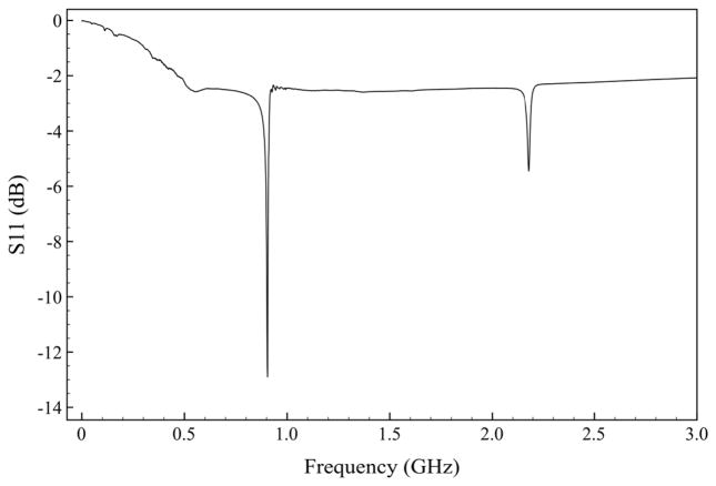
Figure 5 shows the S-parameter characterization of a single FBAR on a glass substrate and blanketed acoustic mirror, demonstrating resonances at fo = 905 MHz and 2.18 GHz, which we attribute to shear and longitudinal resonant modes, respectively, of the device. The acoustic velocities of these modes share a near-identical ratio. The resonant Q, defined here as fo/Δf for FWHM, is 113 for the 905MHz resonance and 129 for the 2.18 GHz resonance. Higher Qs should be achievable with better tuning of the acoustic mirror. The completed structures on CMOS oscillate at a frequency corresponding to the lower-frequency resonance.
Figure 5.
The return loss of an individual FBAR on glass (without de-embedding) shows a high-Q resonant peak at 905 MHz and a second resonant mode at 2.18 GHz. These correspond to the shear and longitudinal resonant modes, respectively, with quality factors of 113 and 129.
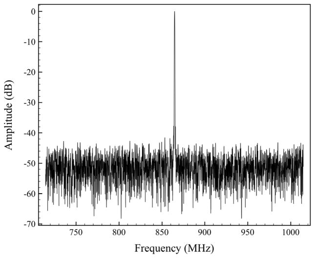
The spectrum at the output of one on-chip FBAR-CMOS oscillator is shown in Figure 6 with a peak at 864.5 MHz. Oscillators across the CMOS array demonstrate a spread of ~10MHz in resonant frequency due to variations in zinc oxide thickness; this variation in no way hinders differential mass measurements, where oscillation frequency is measured both before and after mass addition.
Figure 6.
Output spectrum from monolithic FBAR-CMOS oscillator shows a very sharp resonance at 864.5 MHz.
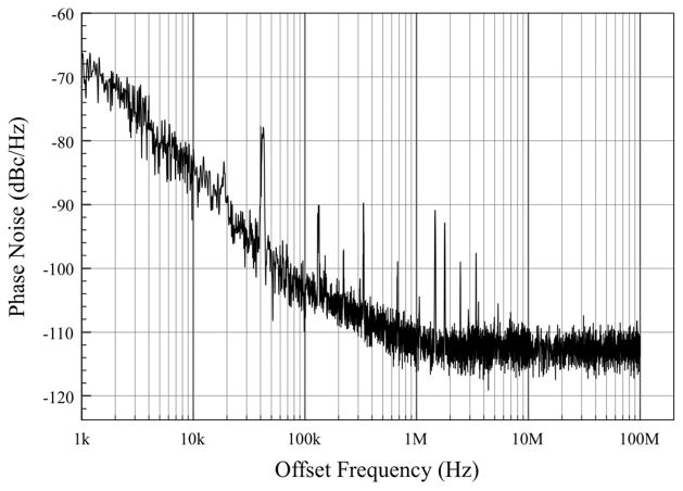
The phase noise performance of an FBAR-CMOS oscillator is shown in Figure 7, demonstrating a measured noise of −83dBc/Hz at an offset of 10kHz and −104dBc/Hz at an offset of 100kHz, both measured from a carrier signal set at the fundamental frequency of oscillation. The relative slope regions of the phase noise plot indicate a Q for the oscillator of 218 in accordance with Leeson’s phase noise relationship [7]. Because the sensor is used as input to a frequency counter, measurement integration can combat the effects of phase noise on measurement resolution.
Figure 7.
The phase noise measurement of an array oscillator shows −83dBc/Hz at an offset of 10kHz and −104dBc/Hz at an offset of 100kHz.
MASS-SENSING
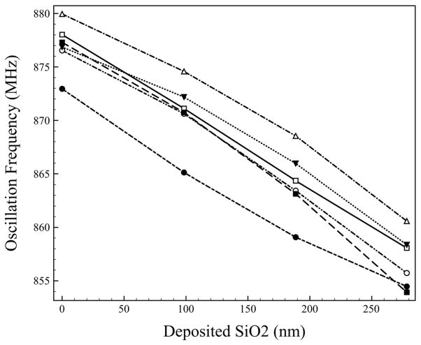
Mass detection is demonstrated in Figure 8 with six different oscillators across the CMOS array. The fundamental oscillation frequency is measured first as a baseline, after which successive layers of patterned silicon dioxide are RF sputtered onto the FBAR top surfaces; frequency measurements are taken after each addition. All oscillators that completed the mass series are shown, while those not depicted failed either before or during the testing process (i.e. did not sustain measurable oscillation). The frequency sensitivity of an FBAR to mass additions is given by the Sauerbrey equation as Δƒ = −(fo2 Δm / NAρ [8] (where ƒo is the operating frequency, Δm is the mass addition, N is the sensitivity constant, A is the active area, and ρ is the density), which predicts a linear change in frequency for small additions of uniform-thickness mass. From Figure 8, we calculate an average mass sensitivity of 3.05×10⁻¹² g/Hz cm2, which is well above the sensitivity of a typical QCM (6×10⁻⁹ g/Hz cm2) [8] and comparable to previous off-chip FBAR sensors [1].
Figure 8.
The mass loading sensitivity is demonstrated on different oscillators in the array; for each oscillator, the resonance decreases linearly with the mass of the deposited silicon dioxide. This data corresponds to a mass sensitivity of 3.3×10¹¹ Hz/ (g cm−2).
CONCLUSION
We have presented a method of monolithic integration of solidly-mounted FBAR structures on an active CMOS substrate. The high operating frequency of FBAR structures is naturally complemented by modern CMOS circuitry. Our integration method allows for a one-chip implementation of a dense array of FBAR-CMOS oscillators without requiring specialized fabrication techniques or non-standard CMOS fabrication processes. The oscillators presented here perform as mass sensors with sensitivity comparable to off-chip FBAR sensors and far in excess of the more traditional quartz crystal microbalance.
This work comprises an array of 24 mass sensors, and the underlying methodology is scalable to allow for denser sensor arrays and higher operating frequencies. The array format lends itself naturally to sensitive, multiplexed chemical and biological detection, and the mass-based sensing mechanism will allow for true label-free analysis.
Acknowledgments
This work was supported in part by the National Institute of Environmental Health Sciences under Grant U01ES016074. The content is solely the responsibility of the authors and does not necessarily represent the official views of the National Institute of Environmental Health Sciences or the National Institutes of Health. This work was also supported in part by the Semiconductor Research Corporation (SRC) Center for Circuit and Systems Solutions (C2S2).
References
- 1.Gabl R, et al. “Novel integrated FBAR sensors: a universal technology platform for bio- and gas-detection,” Sensors. Proc. of IEEE; 22–24 Oct. 2003.2003. pp. 1184–1188. [Google Scholar]
- 2.Otis BP, et al. A 300-μW 1.9-GHz CMOS oscillator utilizing micromachined resonators. IEEE JSSC. 2003 Jul;38(7):1271–1274. [Google Scholar]
- 3.Chee YH, et al. A Sub-100μW 1.9-GHz CMOS Oscillator Using FBAR Resonator. IEEE RFIC Symp. 2005:123–126. [Google Scholar]
- 4.Augustyniak M, et al. An Integrated Gravimetric FBAR Circuit for Operation in Liquids Using a Flip-Chip Extended 0.13μm CMOS Technology. ISSCC Dig Tech Papers. 2007 Feb;:392–393. 610. [Google Scholar]
- 5.Dubois M, et al. Integration of High-Q BAW resonators and filters above IC. ISSCC Dig Tech Papers. 2005 Feb;:392–393. [Google Scholar]
- 6.Aberg, et al. A low noise 0.9 GHz FBAR clock. Analog Integ Circ Sig Proc. 2007;50:29–37. [Google Scholar]
- 7.Leeson DB. A Simple Model of Feedback Oscillator Noise Spectrum. Proc IEEE. 1966 Feb;54:329–330. [Google Scholar]
- 8.Muratsugu M, et al. Quartz crystal microbalance for the detection of microgram quantities of human serum albumin. Anal Chem. 1993 Oct 15;65(20):2933–7. doi: 10.1021/ac00068a036. [DOI] [PubMed] [Google Scholar]


