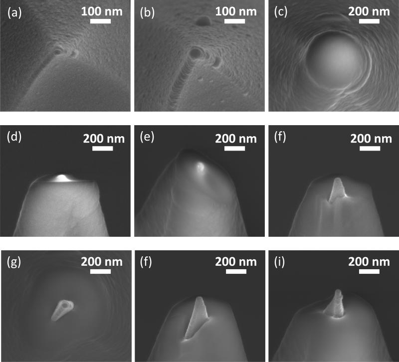
Figure 5.
(a) – (c) SEM images at each deposition step; (a) bare, (b) 5 W biased Cr, and (c) SiO2 deposited tip. The Cr and SiO2 deposition times were 7 and 2 min, which corresponded to 12.2 nm and 255 nm, respectively. (d) – (f) SEM images during different stages of the FEBIE process. (g) – (i) SEM images for the final etched tip; (g) top, (h) 45° tilt, and (i) 90° rotation view.

