Abstract
Electronic self-decoupling of an organic chromophore from a metal substrate is achieved using a naphtalenediimide cyclophane to spatially separate one chromophore unit of the cyclophane from the substrate. Observations of vibronic excitations in scanning tunneling spectra demonstrate the success of this approach. These excitations contribute a significant part of the tunneling current and give rise to clear structure in scanning tunneling microscope images. We suggest that this approach may be extended to implement molecular functions at metal surfaces.
Keywords: electron transport, functional molecules at surfaces, scanning tunneling microscopy, vibronic states
Predictions are difficult, especially about the future. We hope that this truism will be valid for the future of surface science, too. Nevertheless, it appears to be safe to predict that functional molecules at surfaces will be one of the foci of surface science over the next decade. The opportunities in this field are virtually unlimited and range from technological issues such as controlling interface effects in organic devices to adventurous endeavors such as building molecular machines at surfaces. Although these topics are most challenging, the present state of the experimental and theoretical methods of surface science is good reason for optimism that significant scientific progress will be made in this field.
This article focuses on the electronic coupling between molecules and a metal substrate. At the interface, charge transfer and hybridization affect the levels of an adsorbed molecule, which may significantly modify its properties. To recover and use the intrinsic molecular properties, which may be taylored over a wide range, a degree of decoupling from the metallic surface may be desirable. Effective molecular decoupling has been achieved using multilayers of molecules (1) or ultrathin insulating layers (2–5). An alternative approach is to chemically modify a molecule using spacer groups in order to lift a particular subunit from the substrate. With this aim, for instance, bulky groups have been used to preserve switching capability of an azobenzene derivative (6–11). Previously, this approach was used to obtain an electrical insulation of a model molecular wire (12). However, these molecules turned out to be too flexible and thus deformed upon adsorption at metal substrates (13).
Here we use designed cyclophanes to achieve decoupling of one chromophore from a metal surface. These cyclophanes consist of two rigidly separated parallel π-systems from which only one adsorbs to the surface, whereas the second one is expected to remain separated from the metal. Thus, cyclophanes represent a class of molecules that are particularly interesting for investigating columnar π-stacking and through-space or through-bond electronic conductance (14–16). A naphthalenediimide (NDI) cyclophane (Fig. 1) was chosen as a model compound for the present study. It is demonstrated that this organic molecule, with its height of a few angstroms on a metallic substrate, provides sufficient electronic decoupling of the top chromophore to enable detection of vibronic modes in scanning tunneling spectroscopy. These modes give rise to large signals that can be visualized with submolecular resolution in real space.
Fig. 1.
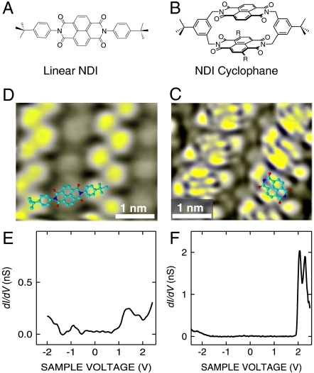
Structural formula of (A) the linear model compound comprising a single NDI chromophore and (B) the NDI cyclophane: R = H, unsubstituted symmetric NDI cyclophane; R = StBu, tert-butyl-thiol substituted NDI cyclophane. Constant-current STM images of (C) asymmetric NDI cyclophanes (I = 50 pA, V = 1.7 V), and (D) the linear NDI model compound (I = 100 pA, V = 1.4 V). Differential conductance (dI/dV) spectrum acquired over (E) a linear NDI and (F) the asymmetric NDI cyclophane. Differential conductance (dI/dV) spectra acquired over the unsubstituted symmetric NDI cyclophane are reported in Supporting Information.
A linear NDI (Fig. 1A) and two NDI cyclophanes (Fig. 1B), an unsubstituted symmetric NDI cyclophane and a tert-butyl-thiol substituted NDI cyclophane, also referred to as asymmetric NDI cyclophane, have been used in the present experiment. The synthesis of various NDI cyclophanes and first scanning tunneling microscope (STM) investigations of unsubstituted symmetric NDI cyclophane on a Au(111) surface have been reported elsewhere (17, 18). The asymmetric NDI cyclophane arranges into large islands composed of periodic parallel rows. Its STM image (Fig. 1C) resembles the appearance of the upper NDI chromophore as can be seen from the superimposed molecular structure. In many experimental runs, linear NDI model compounds deposited on the same surface (Fig. 1D) never showed a similarly detailed resolution of their single chromophore. This observation is consistent with the expectation that the three-dimensional geometry of the cyclophane reduces broadening of the imaged molecular levels. Similarly, the differential conductance spectrum of the linear NDI molecule reported in Fig. 1E shows broad and weak structures at positive and negative voltages, whereas the dI/dV spectrum acquired over the NDI cyclophane (Fig. 1F) shows a clear-cut structure at positive voltages and the onset of a broader feature at the negative voltages. The dI/dV spectrum displays a wide gap of ≈3.3 V, which is comparable to the optical band gap of the unsubstituted NDI chromophore in absorption spectroscopy (≈3.3 eV) (18). Moreover, this gap is substantially larger than the optical gap of tert-butyl-thiol substituited NDI (≈2.3 eV). We thus infer that the cyclophane is oriented with the tert-butyl-thiol substituted NDI at the substrate and the unsubstituted NDI on top, which is also likely because the presence of the thio-ether moieties should favor the adsorption of the substitued NDI on the gold surface. These observations are consistent with the observed similarity of the present STM images with earlier data (17) and with the comparable zero conductance gap and multiple structure of the affinity level in the differential conductance spectra reported in Fig. S1, from unsubstituted symmetric NDI cyclophanes.
We note that a small apparent height difference of ≈0.05 nm between the central lobes of the NDI cyclophane is observed. Geometry optimizations of simplified models for the unattached cyclophane molecule yield two energetically similar conformations with the voluminous tert-butyl groups situated in syn and anti positions relative to the main molecular axis, called C and S shape below. Although the NDI planes enclose an angle of ≈36° in the C conformer, the two chromophore planes are arranged coplanar to each other in the S conformer. The observed height difference and the shape of the individual molecules displayed in Fig. 1C may indicate that the adsorbed cyclophanes adopt a C conformation.
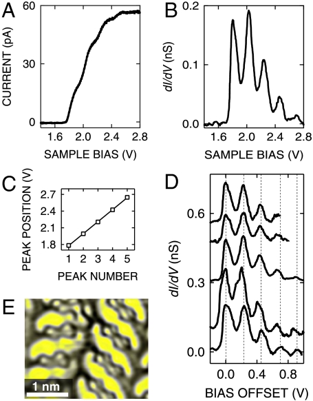
Below we focus on the molecular resonances observed at positive voltage. Fig. 2 A and B displays typical current–voltage characteristics and corresponding differential conductances from this voltage range. The step-like increase of the current corresponds to a series of equidistant peaks of dI/dV. From a linear fit of the peak energies (Fig. 2C) an average spacing of 215 meV is determined. Such spectra acquired over different molecules and at different initial feedback parameters exhibit the same sequence of peaks (Fig. 2D). Additionally, the STM image of the NDI cyclophane displays a remarkably bright S-shaped region between adjacent molecules in the same voltage range (Fig. 2E).
Fig. 2.
(A) I-V characteristics acquired over the NDI cyclophane and (B) corresponding dI/dV spectrum. STM feedback was opened at V = 2.8 V, I = 50 pA. (C) Positions of vibronic peaks versus peak number from the spectrum shown in B. A linear fit was used to evaluate an average peak distance of 215 ± 5 mV. (D) Multiple peaks as in A recorded from different molecules. The data are vertically offset for clarity and shown as a function of the sample bias offset from the position of the lowest-energy peak. Dashed lines indicate the peak spacing in the bottom spectrum. Similar spacings are found in the other spectra from different molecules. STM feedback was opened at I = 50 pA; V = 3 V (first two spectra from bottom), V = 2.8 V (third spectrum), V = 2.6 V (last two spectra from the bottom). The same dataset is reported in the Supporting Information without voltage offset, with the corresponding constant-current STM image. (E) Constant-current STM image of NDI cyclophanes acquired at V = 2.2 V, which corresponds to the most intense vibronic feature in the spectrum shown in B.
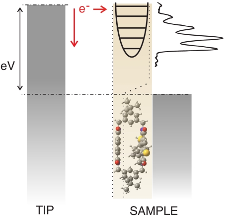
The combination of STM images and spectroscopy suggests a partial decoupling of the top chromophore of the NDI cyclophane. At high positive bias, an electron may resonantly tunnel from the STM tip to an affinity level of the upper NDI chromophore (Fig. 3). Because of the rigid cyclophane structure, coupling with the metal is reduced and tunneling electrons may efficiently couple to vibrational levels of the transiently charged chromophore. We note that an alternative interpretation of the multiple peaks in terms of equidistant molecular orbitals is not expected according to density functional theory (DFT) calculations of free NDI cyclophane molecules (19). An analysis of the near infrared vibrational modes of NDI reveals that an intense vibrational band, which is related to the stretching mode of the C═O bond, has a vibrational energy of ≈205 meV. This value is close to the measured peak spacing of 215 meV. Such vibrational modes are expected to give rise to particularly intense signals in tunneling spectroscopy as they involve a large change of the molecular electric dipole moment upon excitation.
Fig. 3.
Schematic diagram of resonant tunneling to vibronic states at positive sample bias. When the Fermi level of the tip matches a vibronic state a new tunneling channel becomes available, which leads to a peak in dI/dV spectra.
Vibrationally mediated inelastic tunneling usually leads to rather weak variations of the total tunneling current (20). In a number of previous studies, molecules were deposited on ultrathin oxide layers to increase the lifetime of an excited molecular state and somewhat larger signals were obtained. In these cases, coupling to vibronic states of a charged molecule led to equidistant substructures superimposed on intense electronic features (4, 21–23). In the present data from cyclophanes the vibronic structure is particularly clear and intense. It actually dominates the image contrast in conventional constant-current imaging, which may imply extended excited-state lifetimes (24, 25).
The STM image in Fig. 2E was recorded at a sample bias, which corresponds to the most intense maximum of the vibronic structure. Usually, more sophisticated imaging modes such as mapping of d2I/dV2 (20) or photon emission intensities (26) have to be used to visualize the spatial distribution of small inelastic tunneling channels. In contrast, in the present case of cyclophane molecules, vibronic features dominate the contrast in conventional constant-current images, which highlights the extraordinary size of the observed effects. Closer inspection reveals that the vibronic signal is strongest in S-shaped regions between adjacent molecules. This position is the area of the carbon–oxygen double bonds (C═O) of top NDI according to the structure proposed in Fig. 1B.
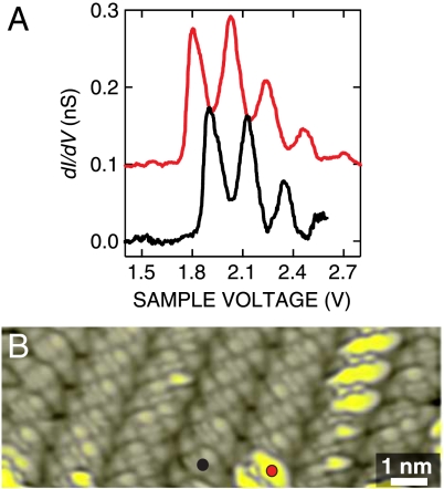
In repeated spectroscopic measurements from NDI cyclophanes, we observed that the onset of the vibronic progression varies to some extent. The examples shown in Fig. 4A demonstrate that shifts of ≈100 meV may occur. An STM image recorded at voltages near the onset (Fig. 4B) visualizes this variability. The variation of the onset from molecule to molecule may be attributed to small differences of the molecular configurations and positions on the Au(111) substrate as well as intermolecular interaction within the layer (27); see also Fig. S2.
Fig. 4.
(A) Differential conductance spectra dI/dV versus sample voltage V. STM feedback was opened at I = 50 pA, V = 2.6 V (black) and V = 2.8 V (red, offset by 0.1 nS for clarity), respectively. (B) Constant-current STM image of the NDI cyclophanes. Tunneling parameters: I = 50 pA, V = 1.8 V.
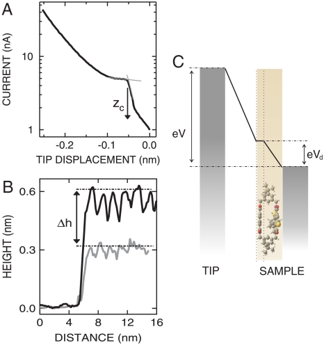
To tune the tunneling rates through the molecular junction, it would be desirable to decrease the tip–molecule distance. The range over which tunneling was observed, however, is surprisingly small, and a contact between the tip and the upper NDI chromophore is formed upon approach of the STM tip toward the molecule. Fig. 5A shows the evolution of the current versus tip displacement, starting from an initial position z0, which is defined by the tunneling parameters used before opening the STM feedback. In Fig. 5A, an exponential current variation, which is typical of tunneling, is observed over a small range of ≈0.05 nm. Next, a rapid rise of the current occurs, which signals the transition to a single molecule contact (28, 29). At contact, further approach of the tip initially has little impact on the current. Up to this point, the current–displacement data are similar to earlier results (30). However, a renewed rise occurs beyond tip displacements of -0.12 nm. Although it will be interesting to analyze in detail this behavior in future work—we hint that it might be linked to the mechanics of the single molecule contact—we now focus on evaluating the distance between the STM tip and the upper NDI chromophore. From the intersection of linear fits to the transition and contact regions, a contact distance zc may be defined (Fig. 5A). We find zc ≈ 0.06 nm. This small extension of the vacuum gap between the tip and the molecule was observed at a sample bias V = 1 V, i.e., within the conductance gap (cf. Fig. 1F). The tip–sample distance increases substantially when resonant tunneling to vibronic states becomes feasible. This is evident from Fig. 5B, which displays the apparent heights of a cyclophane island at V = 1 V and V = 3 V. When the voltage applied to the sample is changed from V = 3 V to V = 1 V, thus approaching the tip, a drastic change of the height, Δh ≈ 0.4 nm, is observed.
Fig. 5.
(A) Semilogarithmic plot of current versus tip displacement acquired over an unsubstituted symmetric NDI cyclophane. Gray thin lines are linear fits to the transition and contact regions. Their intersection is used to define a contact distance zc. Zero displacement (z0) is determined by the parameters (V = 1 V, I = 1 nA) used before opening the STM feedback loop. The contact distance zc is found to be approximately 0.052 ± 0.012 nm, for the conductance curves acquired with an initial setpoint of V = 1 V. (B) Constant-current height profiles acquired of a cyclophane island at I = 50 pA, V = 3 V (black) and I = 1 nA, V = 1 V (gray). (C) Model of the voltage drop across the vacuum gap and the cyclophane. The upper NDI of the cyclophane is lifted from the surface due to the rigid spacers in the cyclophane double structure.
An example of the tip displacement as function of the voltage in a similar voltage range is reported in Fig. S3. Consequently, the overall extension of the vacuum gap, z, can be approximated as the sum Δh + zc.
The above data on the junction geometry show that the vertical extension of the molecule d ≈ 0.5 nm is comparable to size of the vacuum gap at high voltage (V ≈ 3 V). This may result in a variation of the electrostatic potential over the molecule, which in turn would have to be considered in analyzing the spectroscopic features. Indeed, in studies of electron transport through single molecule contacts, the molecular levels are often assumed to float between the Fermi levels of the tip and the sample. In STM, however, molecular levels are usually assumed to be fixed relative to the Fermi level of the sample.
For an estimate of the voltage drop over the cyclophane, we model the junction by a plate capacitor that is partially filled by a dielectric (Fig. 5C). This leads to a voltage drop Vd = (ϵmz/d + 1)-1V, where ϵm is the dielectric constant of the molecule and z is the tip–molecule distance. The molecular height, d ≈ 0.5 nm, is taken from the optimized geometry of the cyclophane (19). ϵm ≈ 28 may be estimated from the molecular polarizability extracted from DFT calculations. Thus, the voltage drop over the molecule can be considered dependent from the vacuum gap extension, z. At tip–molecule distances corresponding to the initial setpoint used in the dI/dV spectra reported in Fig. 2, and owing to the large dielectric constant, a small voltage drop Vd ≈ 0.04 V is obtained, which has little influence on the energy spacing or the onset of the vibronic progression in the reported spectra. The situation is different when voltages within conductance gap are applied. In those cases, due to the extremely small tip–molecule distance, larger voltage drops (≈25% of the applied voltage at V = 1 V) over the molecule are expected, which may influence the apparent onset of the affinity level in the conductance spectra.
Although the above considerations are certainly rather simplistic, they indicate that some voltage drop may occur over the cyclophane, similar to the case of planar molecules on insulating ultrathin films (4, 22). The deviation between the experimentally determined vibrational energy and the DFT result may partially be attributed to this effect.
In summary, a rigid NDI cyclophane was designed to achieve a degree of electronic decoupling of an organic chromophore from a metal substrate. The molecular structure serves to spatially separate one of its two π-electron systems from the substrate. The success of this approach is verified from observations of vibronic excitations in scanning tunneling spectra. Surprisingly, these excitations cause a significant part of the tunneling current and give rise to intense structure in STM images, which therefore reflect the probability of exciting vibrational modes at C═O bonds. We suggest that this approach may be extended to a range of molecules and that it may prove useful in implementing molecular functions, which are familiar from solutions, at metal surfaces.
Material and Methods
The experiments were performed in a homebuilt ultrahigh vacuum scanning tunneling microscope (STM), operated at 5 K. Chemically etched W tips and Au(111) surface were prepared by Ar+ sputtering and subsequent annealing. The molecules, linear NDI and NDI cyclophanes, were deposited from a heated tantalum crucible onto the Au(111) surface kept at room temperature.
For the contact experiments, the status of the tip was checked by indenting into the clean Au(111) surface until the conductance curves showed the expected transition from tunneling to contact regime at a value of 1G0, indicative of a single-atom contact on noble metals (31). To check their reproducibility, more than 150 conductance curves were acquired over the molecules, at different initial position. Geometry optimizations were performed on a density functional level (B3LYP/6-31G*) (32) using Gaussian03 (33).
Supplementary Material
Acknowledgments.
The authors thank T. Gopakumar for helpful discussion. This work was supported by Deutsche Forschungsgemeinschaft via SFB 677, the Innovationsfonds Schleswig-Holstein, the Swiss National Center of Competence in Research “Nanoscale Science,” and the Swiss National Science Foundation.
Footnotes
The authors declare no conflict of interest.
This article is a PNAS Direct Submission.
This article contains supporting information online at www.pnas.org/lookup/suppl/doi:10.1073/pnas.1006661107/-/DCSupplemental.
References
- 1.Dong ZC, et al. Generation of molecular hot electroluminescence by resonant nanocavity plasmons. Nat Photonics. 2010;4:50–54. [Google Scholar]
- 2.Repp J, et al. Molecules on insulating films: Scanning-tunneling microscopy imaging of individual molecular orbitals. Phys Rev Lett. 2005;94:026803. doi: 10.1103/PhysRevLett.94.026803. [DOI] [PubMed] [Google Scholar]
- 3.Ćavar E, et al. Fluorescence and phosphorescence from individual C60 molecules excited by local electron tunneling. Phys Rev Lett. 2004;95:196102. doi: 10.1103/PhysRevLett.95.196102. [DOI] [PubMed] [Google Scholar]
- 4.Qiu XH, Nazin GV, Ho W. Vibronic states in single molecule electron transport. Phys Rev Lett. 2004;92:206102. doi: 10.1103/PhysRevLett.92.206102. [DOI] [PubMed] [Google Scholar]
- 5.Qiu XH, Nazin GV, Ho W. Vibrationally resolved fluorescence excited with submolecular precision. Science. 2003;299:542–546. doi: 10.1126/science.1078675. [DOI] [PubMed] [Google Scholar]
- 6.Alemani M, et al. Electric field-induced isomerization of azobenzene by STM. J Am Chem Soc. 2006;128:14446–14447. doi: 10.1021/ja065449s. [DOI] [PubMed] [Google Scholar]
- 7.Comstock MJ, et al. Reversible photomechanical switching of individual engineered molecules at a metallic surface. Phys Rev Lett. 2007;99:038301. doi: 10.1103/PhysRevLett.99.038301. [DOI] [PubMed] [Google Scholar]
- 8.Kumar AS, et al. Reversible photo-switching of single azobenzene molecules in controlled nanoscale environments. Nano Lett. 2008;8:1644–1648. doi: 10.1021/nl080323+. [DOI] [PubMed] [Google Scholar]
- 9.Piot L, et al. Growth of long, highly stable, and densely packed worm-like nanocolumns of hexa-peri-hexabenzocoronenes via chemisorption on Au(111) J Am Chem Soc. 2008;131:1378–1379. doi: 10.1021/ja808752b. [DOI] [PubMed] [Google Scholar]
- 10.Wolf M, Tegeder P. Reversible molecular switching at a metal surface: A case study of tetra-tert-butyl-azobenzene on Au(111) Surf Sci. 2009;603:1506–1517. [Google Scholar]
- 11.McNellis ER, et al. Azobenzene versus 3,3′,5,5′-tetra-tert-butyl-azobenzene (TBA) at Au(111): Characterizing the role of spacer groups. 2010. arXiv:1002.0687v1. [DOI] [PubMed]
- 12.Moresco F, et al. Contacting a single molecular wire by STM manipulation. Appl Phys A. 2005;80:913–920. [Google Scholar]
- 13.Kuntze J, et al. Conformations of a molecular wire adsorbed on a metal surface. Phys Rev B. 2002;65:233405. [Google Scholar]
- 14.Watson MD, et al. A hexa-peri-hexabenzocoronene cyclophane: An addition to the toolbox for molecular electronics. J Am Chem Soc. 2004;126:1402–1407. doi: 10.1021/ja037520p. [DOI] [PubMed] [Google Scholar]
- 15.Bléger D, et al. Periodic positioning of multilayered [2.2]paracyclophane-based nanopillars. Angew Chem. 2008;120:8540–8543. doi: 10.1002/anie.200801335. [DOI] [PubMed] [Google Scholar]
- 16.Lin HC, Jin BY. Three-dimensional through-space/through-bond delocalization in cyclophane systems: A molecule-in-molecule approach. J Phys Chem A. 2008;112:2948–2954. doi: 10.1021/jp0763127. [DOI] [PubMed] [Google Scholar]
- 17.Gabutti S, et al. A rigid sublimable naphthalenediimide cyclophane as model compound for UHV STM experiments. Chem Commun. 2008;20:2370–2372. doi: 10.1039/b719796a. [DOI] [PubMed] [Google Scholar]
- 18.Gabutti S, et al. Planar chiral asymmetric naphthalenediimide cyclophanes: Synthesis, characterization and tunable FRET properties. Org Biomol Chem. 2009;7:3222–3229. doi: 10.1039/b905945h. [DOI] [PubMed] [Google Scholar]
- 19.Knutzen M. Kiel, Germany: Universität Kiel; 2007. Electronic structure of functionalized organic molecules adsorbed on Au(111) Diploma thesis. [Google Scholar]
- 20.Stipe BC, Rezaei MA, Ho W. Single-molecule vibrational spectroscopy and microscopy. Science. 1998;280:1732–1735. doi: 10.1126/science.280.5370.1732. [DOI] [PubMed] [Google Scholar]
- 21.Nazin GV, Wu SW, Ho W. Tunneling rates in electron transport through double-barrier molecular junctions in a scanning tunneling microscope. Proc Natl Acad Sci USA. 2005;102:8832–8837. doi: 10.1073/pnas.0501171102. [DOI] [PMC free article] [PubMed] [Google Scholar]
- 22.Ogawa N, Mikaelian G, Ho W. Spatial variations in submolecular vibronic spectroscopy on a thin insulating film. Phys Rev Lett. 2007;98:166103. doi: 10.1103/PhysRevLett.98.166103. [DOI] [PubMed] [Google Scholar]
- 23.Pradhan NA, Liu N, Ho W. Vibronic spectroscopy of single C60 molecules and monolayers with the STM. J Phys Chem B. 2005;109:8513–8518. doi: 10.1021/jp045289b. [DOI] [PubMed] [Google Scholar]
- 24.Braig S, Flensberg K. Vibrational sidebands and dissipative tunneling in molecular transistors. Phys Rev B. 2003;68:205324. [Google Scholar]
- 25.Galperin M, Nitzan A, Ratner MA. Resonant inelastic tunneling in molecular junctions. Phys Rev B. 2006;73:045314. [Google Scholar]
- 26.Schull G, Becker M, Berndt R. Imaging confined electrons with plasmonic light. Phys Rev Lett. 2008;101:136801. doi: 10.1103/PhysRevLett.101.136801. [DOI] [PubMed] [Google Scholar]
- 27.Kröger J, et al. Molecular orbital shift of perylenetetracarboxylic-dianhydride on gold. Chem Phys Lett. 2007;438:249–253. [Google Scholar]
- 28.Chen F, et al. Measurement of single-molecule conductance. Annu Rev Phys Chem. 2007;58:535–564. doi: 10.1146/annurev.physchem.58.032806.104523. [DOI] [PubMed] [Google Scholar]
- 29.Berndt R, Kröger J, Néel N, Schull G. Controlled single atom and single molecule contacts. Phys Chem Chem Phys. 2010;12:1022–1032. doi: 10.1039/b908672m. [DOI] [PubMed] [Google Scholar]
- 30.Wang YF, et al. Atomic-scale control of electron transport through single molecules. Phys Rev Lett. 2010;104:176802. doi: 10.1103/PhysRevLett.104.176802. [DOI] [PubMed] [Google Scholar]
- 31.Kröger J, Néel N, Limot L. Contact to single atoms and molecules with the tip of a scanning tunnelling microscope. J Phys Condens Matter. 2008;20:223001. [Google Scholar]
- 32.Becke AD. Density-functional thermochemistry. III. The role of exact exchange. J Chem Phys. 1993;98:5648–5652. [Google Scholar]
- 33.Frisch MJ, et al. Wallingford, CT: Gaussian Inc.; 2004. Gaussian 03, Revision C02. [Google Scholar]
Associated Data
This section collects any data citations, data availability statements, or supplementary materials included in this article.


