Abstract
We fabricated ZnS nanocrystals decorated single-walled carbon nanotube (SWNT) based chemiresistive sensor for DNA. Since the charge transfer in the hybrid nanostructures is considered to be responsible for many of their unique properties, the role of ZnS nanocrystals toward its performance in DNA sensor was delineated. It was found that the free carboxyl groups surrounding the ZnS nanocrystals allowed large loading of single strand DNA (ssDNA) probe that provided an ease of hybridization with target complementary c-ssDNA resulting in large electron transfer to SWNT. Thus it provided a significant improvement in sensitivity toward c-ssDNA as compared to bare SWNT based DNA sensor.
Recent advances have resulted in the large-scale preparation of relatively monodisperse quantum dots (QDs). Compared with existing labels, nanoparticles in general and QD in particular are more stable and cheaper. These QDs are widely used in photocatalysis,1 luminescence,2, 3 and bioconjugate.4, 5 Recent advances in nanomaterials have generated a class of markers and probes by conjugating semiconductor QDs with biomolecules that have affinities for binding with selected biological structures. Recently, the carboxyl group functionalized ZnS QDs have been utilized as a reagentless amperometric uric acid biosensor.6 Its ability to promote the direct electron transfer between the biomolecules and electrode surfaces was also explored.7
Field-effect transistors (FETs) based on semiconductor CNTs have attracted much interest due to their superior properties such as high conductance, high mobility, and chemical inertness, compared to ones based on conventional semiconductor materials. A great deal of effort was placed on using single-walled carbon nanotubes for electrochemical sensor design. Nowadays, a great deal of research efforts has been devoted to alter the physical properties of CNTs by surface modification with organic, inorganic, and biological species.8, 9 Among them, linking semiconductor nanocrystals to CNTs has emerged as an active field.10, 11 The superiority of this system lies in the fact that the combination of the properties of two functional nanoscale materials can be used to achieve a wider range of applications. With the development of electrochemical DNA sensors, it is necessary to search for efficient surface-immobilization techniques to enhance immobilization amount and ultimate detection capacity of sequence specific DNA. A detection method of DNA hybridization based on labeling with QD tracers has been developed with electrochemical-stripping measurements of the nanoparticles.12, 13 Kong et al.14 have proposed a mechanism for the interaction of SWNTs and DNA using first principle electronic structure calculations. Functionalizing CNTs with ZnS nanocrystals cannot only combine the advantages of ZnS (n-type semiconductor) and single-walled carbon nanotube (SWNT) (p-type semiconductor) but also may result in fresh properties, which have potential applications in nanoscale electronic devices.
In this work, the electrical and DNA sensing properties of ZnS nanocrystals functionalized SWNTs were systematically investigated to develop a better understanding of the sensing mechanism by the measurement of I−V and FET transfer characteristics.
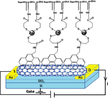
Oligonucleotide NH2-ssDNA (5′amino-GAGCGGCGCAACATTTCAGGTCGA-3′) and its complementary c-ssDNA (5′TCGACCTGAAATGTTGCGCCGCTC-3′) and noncomplimentary nc-ssDNA (5′CAGCGGCGCAACATTTCAGGTCGA-3′) were purchased from MWG Biotech Pvt. Ltd. Bangalore, India. The SWNTs (SWNT-COOH, 80%–90% purity; bundle diameter: 4–5 nm) were purchased from Carbon Solution, Inc. (Riverside, CA). The SWNTs (0.01 mg ml−1) were suspended in N,N-dimethylformamide (DMF) and were ultrasonically dispersed by centrifugation at 31000×g for 90 min. The dispersed SWNTs were aligned across a pair of the 3 μm apart microfabricated gold electrodes by ac dielectrophoresis by applying 0.36 VRMS at 4 MHz frequency until a desired resistance was achieved, followed by annealing at 300 °C for 1 h in a reducing environment (i.e., 5% H2 in N2).15 The aligned SWNTs were incubated in a 6 mM solution of 1-pyrenemethylamine hydrochloride (PyMe-N H2) in DMF, for 2 h, at room temperature, washed extensively with DMF and dried under N2. The whole assembly was then treated with 6 mM 6-mercapto-1-hexanol (MCH) in DMF to block the nonspecific binding site at gold surface for 1 h. An aqueous solution of mercaptopropeonic acid (MPA) caped ZnS nanocrystals of 5–6 nm size was prepared by procedure as reported earlier16 for further ZnS functionalization of SWNTs. 1-pyrenemethylamine functionalized aligned SWNTs were treated with 1 mg ml−1 aqueous solution of ZnS (MPA) nanocrystals containing 0.1M N-(3-dimethylaminopropyl)- N′ -ethyl carbodiimide and 0.05MN-hydroxy succinamide for 2 h and was rinsed thoroughly with double distilled water. ss-DNA probe was covalently immobilized on ZnS functionalized SWNTs by depositing a drop of 1 μM NH2-ssDNA in phosphate buffer solution (PBS) (0.01M; pH 7.2) on the chip for 20 h, at 37 °C in an incubator. To remove the loosely bound ss-DNA, the SWNTs were washed five times with PBS and dried under N2. The ZnS∕SWNTs FET was formed by using the highly doped silicon substrate as a back gate and is schematically represented in Fig. 1. NH2-ssDNA was covalently immobilized directly over the aligned SWNT through 1-pyrene butanoic acid succinimidyl ester (PyBtNHS) without undergoing any functionalization with ZnS nanocrystals to fabricate SWNTs FET for comparative study. DNA hybridization was carried out with c-ssDNA, on the device chip.
Figure 1.
Schematic cross-section of the ZnS∕SWNT FET device.
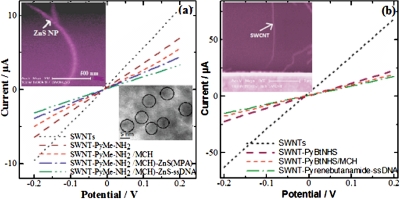
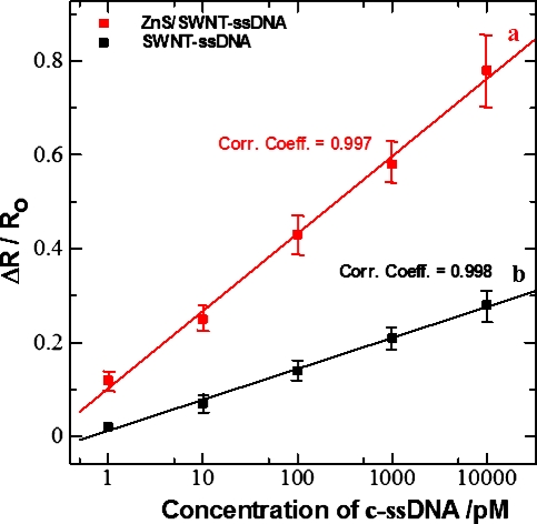
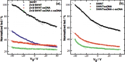
The fabrication and sensing processes were monitored by recording the current-voltage (I-V) characteristics of the device between +1 and −1 V after each step using a HP4155A semiconductor parameter analyzer and taking the inverse of the slope of the I−V curve from −0.1 to+0.1 V. As shown in Fig. 2, the current in the SWNTs device at a given voltage decreased upon functionalization with 1-pyrenemethylamine∕1-pyrene butanoic acid succinimidyl ester, which is due to π-π stacking interactions between SWNTs and pyrene groups. The current in SWNT device further decreased upon treatment with nonspecific blocking reagent MCH, functionalization with ZnS (MPA) nanocrystals and NH2-ssDNA hybridization [Fig. 2a]. These changes in resistance are attributed to the reduction in the charge carriers (holes) in the p-type semiconductor SWNT from an accumulation of negative charge and∕or scattering potential as a result of covalent attachment of ZnS nanocrystals to SWNTs and of NH2-ssDNA to ZnS and modulation of work function difference between the metal (gold) contacts and semiconducting SWNTs. The surface characterization of SWNTs device by scanning electron microscope (Philips XL30 FEG) also confirmed the attachment of preformed 4–5 nm size ZnS nanocrystals [as evident by transmission electron microscope (TEM)] over SWNT [see inset of Fig. 2a]. It is noteworthy to observe that the ZnS nanocrystals are well decorated with equal interspacing over the aligned SWNT resulting in the formation of multiple p-n junction type semiconductor devices. However, to understand the role of ZnS nanocrystals over SWNT for DNA detection, we have fabricated a similar SWNT device without ZnS nanocrystals [Fig. 2b] and have undertaken a comparative DNA sensing study. The current∕resistance behavior of both the devices was monitored for different concentrations of c-ssDNA and nc-ssDNA, respectively. As expected, both the devices did not show any significant change in current resistance response toward nc-ssDNA because of no hybridization due to mismatch of the nc-ssDNA sequence with the probe ss-DNA (data not shown). Moreover, the devices responded explicitly for different concentrations of c-ssDNA due to hybridization. All experiments for monitoring the device response toward c-ssDNA were carried out after incubation with different concentration of c-ssDNA, for 5 min, followed by washing and then drying under N2. Figure 3 shows a calibration curve of devices with and without ZnS nanocrystals. As shown in Fig. 3, both devices exhibited a linear change in the response (normalized resistance change) upon incubation with c-ssDNA from 1 pM to 10 nM concentrations. However, a significant difference in sensitivity was observed between the two devices. The ZnS∕SWNT-ssDNA device exhibited about 2.5 fold increase in sensitivity of 0.16 per decade pM c-ssDNA (the slope of the calibration curve) over SWNT-ssDNA device showing a sensitivity of 0.06 per decade pM c-ssDNA. This significant increase in sensitivity toward c-ssDNA hybridization may be attributed to an increased loading of NH2-ssDNA probe over ZnS nanocrystals due to their large surface to volume ratio and a subsequent transfer of negative charge electrons to SWNT upon hybridization with c-ssDNA. To further understand the sensing mechanism, we have done a FET study. Figures 4a, 4b show typical gate voltage dependence of the normalized Isd for ZnS∕SWNT and SWNT, devices, respectively, after functionalization with the capture ss-DNA probe and after hybridization with 1 nM c-ssDNA. It was observed that percentage Isd decreased with the covalent attachment of ZnS nanocrystals over SWNT, as it doped SWNT heavily with negative charge electrons. The decrease in hole density in SWNT was calculated by using a widely used expressionCΔVT∕eL, where C is the approximate capacitance, ΔVTis the shift in threshold voltage, ethe electron charge, and L the channel length17 and the field-effect mobility of the holes was calculated in the linear regime by the equation, μ=(L)2 (dIsd∕dVg)∕ CVD, wherein VD is the drain voltage.18 The device revealed a decrease in holes concentration by 2.7×106 cm−1 after the ZnS attachment, as the threshold voltage was shifted to negative side by 1.8 V with respect to bare SWNT. The device exhibits a charge mobility of ∼8×102 cm2∕V s after ZnS functionalization of bare SWNT. A further decrease in Isd and charge mobility as well, was found after the immobilization of ss-DNA probe over the ZnS nanocrystals in the ZnS∕SWNT device. The hole density was decreased by ∼8.3×106 cm−1 due a threshold voltage shift of 5.3 V and the charge mobility was significantly decreased to∼2.2×102 cm2∕V s. This significant feature of the device indicates a Schottky barrier mechanism [(Fig. 4a] which may be due to the fact that the adsorbed biomolecule at the metal contact modulate the local work function and thus the band alignment.19 After hybridization with c-ssDNA, the device shows a further decrease in hole density by ∼1.0×107 cm−1 versus ZnS∕SWNT-ssDNA due to a threshold voltage shift of 6.8 from −8.59 to −15.59 V due to a negative charge doping of SWNT resulting in decrease of hole density in SWNT. Similarly, a large decrease in charge mobility was seen from ∼2.2×102 cm2∕V s obtained in ZnS∕SWNT-ssDNA to ∼1.2×102 cm2∕V s in ZnS∕SWNT-ssDNA-c-ssDNA, which is a net decrease of ∼1.0×102 cm2∕V s upon hybridization.
Figure 2.
I-V characteristics of the device at various stages of fabrication (a) ZnS∕SWNT (b) SWNT; upper left side inset: SEM of ZnS∕SWNT and SWNT, and bottom right side inset: TEM of ZnS.
Figure 3.
Calibration curve of (a) ZnS∕SWNT-ssDNA and (b) SWNT-ssDNA sensor for complimentary DNA (c-ssDNA). Data points are averages of four independent sensors (for each investigation) prepared at different times, and error bars represent ±1 standard deviation.
Figure 4.
Typical gate voltage dependence of the normalized source-drain current Isd at VD of 0.5 V for (a) ZnS∕SWNT device, immobilized with probe-ssDNA and hybridized with c-ssDNA and (b) bare SWNT device, immobilized with probe-ssDNA and hybridized with c-ssDNA.
On comparing the charge transfer characteristic of ZnS∕SWNT device with that of SWNT, it has been found that though the sensing mechanism in SWNT device is also governed by electrostatic gating effect but no major change in charge mobility was found in SWNT. The hole density was decreased by 6.8×106 cm−1 due a threshold shift of 4.5 V upon hybridization, which is smaller than the value obtained in ZnS∕SWNT device. A very small change in charge mobility was seen upon ssDNA probe immobilization and on subsequent hybridization step, i.e., ∼6–6.5×102 cm2∕V, as can be seen from the slope dI∕dV [Fig. 4b]. This further corroborates our contention that the improved sensitivity of ZnS∕SWNT device toward target c-ssDNA is due higher loading of ssDNA probe over the large negative charged binding sites of ZnS nanocrystals and successive large electron doping on SWNT on hybridization with c-ssDNA.
In conclusion, we have fabricated ZnS nanocrystals decorated SWNT FET device for DNA detection. We have discussed in detail the role of ZnS nanocrystals in sensing mechanism toward target DNA. An analysis of the transfer characteristic of the FET suggests that the ZnS nanocrystals provides high loading of ssDNA probe and the sensing mechanism is governed by strong electrostatic gating effect with large electron doping on SWNT, resulting in improved sensitivity toward c-ssDNA detection in comparison to SWNT FET. Such improvement could make this device important for those nanobiosensors that demand high performance.
Acknowledgments
A.M. acknowledges the support of grants from NSF (Grant No. CBET-0617240) and NIH (Grant No. U01ES016026). Rajesh is thankful to Indo-U.S. Science and Technology Forum (IUSSTF), New Delhi, India for providing a research fellowship. S.S. acknowledge the Thai Government Scholarship (Ministry of Science and Technology, Thailand).
References
- Nakaoka Y. and Nosaka Y., Langmuir 13, 708 (1997). 10.1021/la960155d [DOI] [Google Scholar]
- Thantu N., J. Lumin. 111, 17 (2005). 10.1016/j.jlumin.2004.06.002 [DOI] [Google Scholar]
- Chen Y. and Rosenzweig Z., Nano Lett. 2, 1299 (2002). 10.1021/nl025767z [DOI] [Google Scholar]
- Bruchez M., Moronne M., Gin P., Weiss S., and Alivisatos A. P., Science 281, 2013 (1998). 10.1126/science.281.5385.2013 [DOI] [PubMed] [Google Scholar]
- Ding S. Y., Jones M., Tucker M. P., Nedeljkovic J. M., Wall J., Simon M. N., Rumbles G., and Himmel M. E., Nano Lett. 3, 1581 (2003). 10.1021/nl034578t [DOI] [Google Scholar]
- Zhang F., Li C., Li X., Wang X., Wan Q., Xian Y., Jin L., and Yamamotob K., Talanta 68, 1353 (2006). 10.1016/j.talanta.2005.07.051 [DOI] [PubMed] [Google Scholar]
- Lu Q., Hu S. S., Pang D. W., and He Z. K., Chem. Commun. (Cambridge) 2005, 2584. 10.1039/b501401h [DOI] [PubMed] [Google Scholar]
- Li Q. W., Sun B. Q., Kinloch I. A., Zhi D., Sirringhaus H., and Windle A. H., Chem. Mater. 18, 164 (2006). 10.1021/cm0512575 [DOI] [Google Scholar]
- Shi D., Lian J., Wang W., Liu G., He P., Dong Z., Wang L., and Ewing R. C., Adv. Mater. 18, 189 (2006). 10.1002/adma.200501680 [DOI] [Google Scholar]
- Banerjee S. and Wong S. S., J. Am. Chem. Soc. 125, 10342 (2003). 10.1021/ja035980c [DOI] [PubMed] [Google Scholar]
- Zhao L. P. and Gao L. J., J. Mater. Chem. 14, 1001 (2004). 10.1039/b315450e [DOI] [Google Scholar]
- Wang J., Liu G., Polsky R., and Merkoçi A., Electrochem. Commun. 4, 722 (2002). 10.1016/S1388-2481(02)00434-4 [DOI] [Google Scholar]
- Wang J., Liu G., and Merkoçi A., J. Am. Chem. Soc. 125, 3214 (2003). 10.1021/ja029668z [DOI] [PubMed] [Google Scholar]
- Kong K. J., Chang H., and Lee J. O., Technical Proceedings of the 2007, NSTI Nanotech Conference, Santa Clara, CA, 2007, Vol. 1, p. 532.
- Lim J. -H., Phiboolsirichit N., Mubeen S., Rheem Y., Deshusses M. A., Mulchandani A., and Myung N. V., Electroanalysis 22, 99 (2010). [Google Scholar]
- Li H., Shih W. Y., and Shih W. -H., Nanotechnology 18, 205604 (2007). 10.1088/0957-4484/18/20/205604 [DOI] [PubMed] [Google Scholar]
- Li C., Lei B., Zhang D., Liu X., Han S., Tang T., Rouhanizadeh M., Hsiai T., and Zhou C., Appl. Phys. Lett. 83, 4014 (2003). 10.1063/1.1625421 [DOI] [Google Scholar]
- Lim J. -H., Phiboolsirichit N., Mubeen S., Deshusses M. A., Mulchandani A., and Myung N. V., Nanotechnology 21, 075502 (2010). 10.1088/0957-4484/21/7/075502 [DOI] [PubMed] [Google Scholar]
- Heller I., Janssens A. M., Mannik J., Minot E. D., Lemay S. G., and Dekker C., Nano Lett. 8, 591 (2008). 10.1021/nl072996i [DOI] [PubMed] [Google Scholar]


