

Abstract
Electronics that are capable of intimate, non-invasive integration with the soft, curvilinear surfaces of biological tissues offer important opportunities for diagnosing and treating disease and for improving brain-machine interfaces. This paper describes a material strategy for a type of bio-interfaced system that relies on ultrathin electronics supported by bioresorbable substrates of silk fibroin. Mounting such devices on tissue and then allowing the silk to dissolve and resorb initiates a spontaneous, conformal wrapping process driven by capillary forces at the biotic/abiotic interface. Specialized mesh designs and ultrathin forms for the electronics ensure minimal stresses on the tissue and highly conformal coverage, even for complex curvilinear surfaces, as confirmed by experimental and theoretical studies. In vivo, neural mapping experiments on feline animal models illustrate one mode of use for this class of technology. These concepts provide new capabilities for implantable or surgical devices.
Strategies for bio-integrated electronics must overcome the challenges associated with the mismatch between the hard, planar surfaces of semiconductor wafers and the soft, curvilinear tissues of biological systems. These differences in mechanics and form lead, almost invariably, to low fidelity coupling at the biotic/abiotic interface and limited long-term tissue health. The difficulties are most pronounced, and the solutions are perhaps most important, in systems designed for brain-computer interfaces (BCIs). State of the art penetrating microelectrode arrays consist of sharp shanks, typically, 10×10 arrays of pins with base widths ~80 μm, lengths ~1.5 mm and pitch ~400 μm1. These arrays are rigid and inflexible due to their construction from blocks of silicon, which also supports their conventional wafer-based electronics. They are valuable for research in BCI, but they damage tissue and do not offer long-term electrical interface stability2 due to unwanted biological responses to the electrodes. Comparable BCI performance can be achieved with non-penetrating, surface electrode systems that are minimally-invasive and provide greatly improved stability3–5 with minimized inflammation. Standard clinical subdural electrode arrays are useful for BCI6 but their widely spaced (~1 cm), large contact electrodes (~0.35 cm diameter) spatially undersample the electrical signals present on the surface of the brain7. Decreasing the spacing and size of the measurement points can improve BCI performance by providing access to high temporal and spatial frequency signals8. Such designs, however, demand excellent conformal coverage over the highly convoluted brain surface, to ensure direct coupling between brain tissue and the electrodes.
Reducing the thickness of the substrate decreases the bending rigidity, thereby improving conformal contact. Unfortunately, clinical arrays and even the thinnest devices designed for research have thicknesses (700 μm and >10 μm9, 10, respectively) that are larger than desired to ensure conformal contact. Analogous systems based on stretchable substrates have also been explored in other neural interfaces11, 12 but typically with similar or larger thicknesses. In conventional designs, ultrathin geometries (i.e. < 10 μm) are impractical, because the films are not sufficiently self-supporting to be manipulated effectively during fabrication or implantation.
Silk is an appealing biopolymer for this application because it is optically transparent13, 14, mechanically robust and flexible in thin film form15–17, compatible with aqueous processing18, 19, amenable to chemical and biological functionalization13, 20. The silk, in both the non-treated and ethanol treated formats, is biocompatible21, 22, bioresorbable23, and water soluble with programmable rates of dissolution15, 16. In addition, recent work demonstrates the ability of silk films to serve as a platform for transistors23 and various classes of photonic devices24, 25. The process of preparing silk substrates for the purposes reported here began with material derived from Bombyx mori cocoons, and followed published procedures18, 19. Briefly, boiling the cocoons in a 0.02 M aqueous solution of sodium carbonate for 60 minutes removed sericin, a water-soluble glycoprotein that binds fibroin filaments in the cocoon but can induce undesirable immunological responses21, 26. An aqueous solution of lithium bromide at 60°C solubilized the fibers and subsequent dialysis removed the lithium bromide. Centrifugation followed by micro-filtration eliminated particulates to yield solutions of 8–10 % silk fibroin with minimal contaminants. Casting a small amount of the solution on a flat piece of poly(dimethylsiloxane) (PDMS) followed by crystallization in air (~12 h) yielded uniform films (thickness of 20–50 μm) (Fig 1a) that were subsequently removed from the PDMS for integration with separately fabricated electronics.
Figure 1. Schematic illustration and images corresponding to steps for fabricating conformal silk-supported PI electrode arrays.
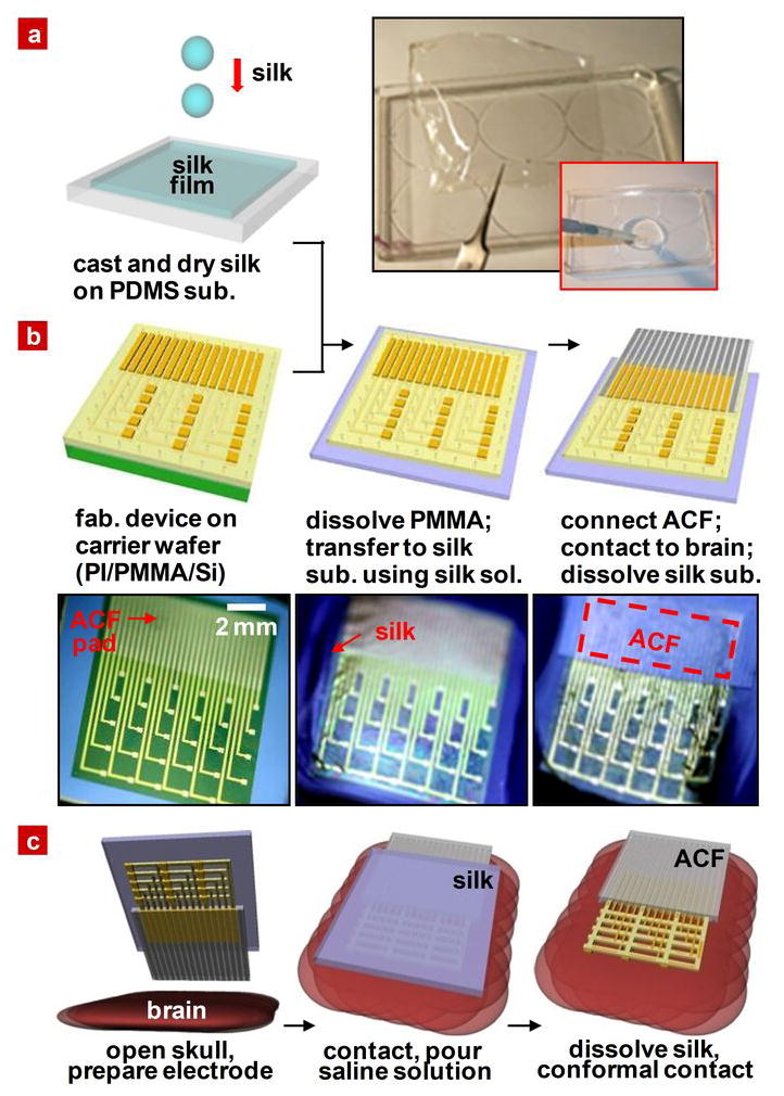
a, Casting and drying of silk fibroin solution on a temporary substrate of PDMS; 5–15 μm thick silk film after drying for 12 hours at room temperature. b, Steps for fabricating the electrode arrays, transfer printing them onto silk, and connecting to ACF cable. c, Schematic illustration of clinical usage of a representative device in an ultrathin mesh geometry with dissolvable silk support.
For the systems described in the following, polyimide (PI) served as a support for arrays of electrodes designed for passive neural recording. Control devices consisted of otherwise similar layouts, but formed using standard photolithographic procedures applied directly on commercial PI films (Kapton, DuPont, USA) with thicknesses of 25 and 75 μm (Fig S1). Anisotropic conductive film (ACF) bonded to electrode pads at one end of the arrays provided electrical connection to external data acquisition systems (Fig S2). Ultrathin PI films, with or without mesh layouts, cannot be manipulated effectively for processing, interconnecting or implanting onto the brain due to their extreme flexibility and mechanical fragility. For these cases, the fabrication process exploited layers of PI spin cast onto silicon wafers coated with sacrificial films of poly(methylmethacrylate) (PMMA) (left frame of Fig 1b). After electrode fabrication, the mesh structure devices underwent further etching to remove unwanted parts of the PI. The processing was completed by dissolving the PMMA layer with acetone, transfer printing the entire assembly to a film of silk and connecting the ACF, yielding easily manipulated bioresorbable neural recording systems. See schematic illustrations and images of Fig. 1b. In all cases, the electrode arrays consisted of 30 measurement electrodes (Au, 150 nm) in a 6 × 5 configuration, each with dimensions of 500 μm × 500 μm and spaced by 2 mm. Interconnection wires to each electrode were protected by a thin (~1.2 μm) overcoat of PI to prevent contact with the tissue or surrounding fluids. Choosing the thickness of the PI passivation layer to match that of the PI substrate locates the gold electrode at the neutral mechanical plane, thereby minimizing the potential for bending-induced mechanical fracture. Details of the fabrication steps appear in the methods section. Electrode arrays were implanted by placing them on the exposed brain (after craniotomy) and then flushing with saline to dissolve the silk, simulating immersion in cerebral spinal fluid. This procedure induced spontaneous, conformal wrapping of the device, as illustrated schematically for the mesh design in Fig. 1c. After the required measurement, the electrode array can be easily removed, due to attachment of the electrodes to the ACF.
The sequence of images in Fig. 2a shows the dissolution process for a representative case (7 μm thick PI film, connected to ACF on a silk substrate with thickness of ~25 μm) inserted into warm water (~35 °C). As the silk substrate disappears, the total bending stiffness, EI, diminishes dramatically due to its cubic dependence on thickness. Computed results appear in Fig 2b and Fig S3c for PI thicknesses of 2.5 and 7 μm. To highlight the benefits of reduced thickness, the inset shows the ratio of EI for these two cases. Through programmed control of the dissolution rate via modifications of the silk protein secondary structure15, 16, these changes in EI can be designed to occur over periods of time ranging from seconds to years, depending on requirements. Figure 2c shows, as an example, the dissolution rate of silk film slightly treated with ethanol (left frame) and computed time dependence of EI in devices that employ more thorough ethanol treatment (right frame). The error range for silk thickness measurement is ± 7%. See SI for detailed conditions. This dissolution time can be lengthened even more by extending the treatment time to days or weeks15; the corresponding time dependence of EI appears in Fig S4.
Figure 2. Time dependent changes as the silk substrate dissolves.

a, Dissolution of the silk via submersion in warm water. b, Total bending stiffness of 7 μm and 2.5 μm electrode arrays on supporting silk films as a function of thickness of the supporting silk film; inset shows the ratio of bending stiffness between 7 μm and 2.5 μm. c, Time dependent change in volume of a silk film during dissolution (left frame) and bending stiffness calculated for silk treated in 70% ethanol for 5 seconds for two different array thicknesses (right frame). The 5 second ethanol treatment increases the dissolution time from minutes to about 1 hour.
To examine the ability of these systems to conform to relevant surfaces, we performed experiments using a human brain model, following the basic steps shown in Fig. 1c. Figure 3 provides images for various cases after washing with saline, including relatively thick control devices that do not incorporate silk. Clearly, the extent of conformal coverage increases with decreasing thickness; the mesh design provides further improvements, as shown in Fig. 3d, S5 and S6. To reveal the underlying mechanics, we performed systematic and quantitative studies on well defined surfaces that capture certain basic features of the curvature of the brain. The first set of experiments explored wrapping the devices on isolated and overlapped cylindrical surfaces. Figure 4a shows the simplest case of a device with bending stiffness EI, thickness h, width b and length 2L, wrapped on a cylinder with radius R. Analytical expressions for EI can be written for the multilayer structures of Fig. 1 in terms of material properties and geometries, as described in the SI. For the wrapped state to be energetically favorable,
Figure 3. Neural electrode arrays of varying thickness on simulated brain models to illustrate flexibility.
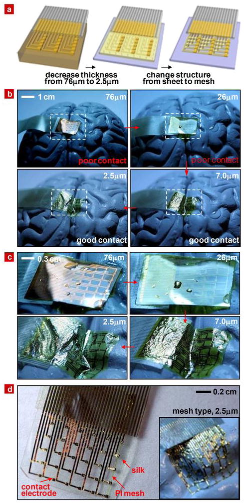
a, Schematic illustration of trends in thickness and structure that improve conformal contact. b, Series of pictures illustrating how the thickness of the electrode array contributes to conformal contact on a brain model. c, Magnified view of these pictures. d, Image of an electrode array with a mesh design on dissolvable silk substrate. Arrows indicate struts in the mesh that help to stabilize the Au interconnects after dissolution of the silk. The inset illustrates the high degree of conformal contact that can be achieved on the brain model once the silk substrate has been dissolved.
Figure 4. Mechanical modelling, theoretical predictions and measured properties.

a, A thin film wrapped around a cylinder of radius R. The unwrapped and wrapped states appear in the top and center frames, respectively. The bottom frame compares the mechanics model and experiments. b, A thin film wrapped around two overlapped cylinders. The top and center frames show the unwrapped and wrapped states, respectively. The bottom frame shows a comparison between the mechanics model and experiments. c, Images of electrode arrays (76 μm sheet in left top, 2.5 μm sheet in right top and 2.5 μm mesh in bottom panel) wrapped onto a glass hemisphere. d, Mechanics models for sheet (left frame) and mesh (right frame) designs.
| (1) |
where γ is the adhesion energy per unit area. The bottom frame of Fig. 4a compares the above relation with a series of experiments (Fig. S7). The data, whose error range is ± 5%, are consistent with γ ~10 mJ/m2, which is comparable to reported values for wet interfaces27. Reducing the thickness provides clear benefits, e.g. wrapping cylinders using only capillary adhesion forces is possible for R ~1 cm when h < ~15 μm.
A pair of overlapped cylinders represents a simple model for a gyrus of the brain. Figure 4b shows cylinders with radii R, a center-to-center separation of 2d and connected by a smooth arc of radius r0, at the angular position θ0 = sin−1[d/(R + r0)]. The contact angle of thin film with one cylinder θ can be shown to be
| (2) |
where γc is given in Eq. (1). The solution of equation (2) takes the form θ = θ(d/R, γ/γc). For γ < γc, the energy has a minimum at θ = 0, and the film does not wrap around the cylinders. Partial wrapping occurs to a contact angle of θ (i.e. contact for angles between 0 and θ < θ0) for , where is obtained from Eq. (2) with θ = θ0 as given in SI. For , wrapping is complete (i.e. conformal contact for angles between 0 and θ0). By comparing Eq. (2) with the experiment in Fig. S8, the extracted adhesion energy per unit area is γ = 10mJ m2. Results appear in the bottom frame of Fig. 4b, where the parameters correspond roughly to features on the brain model: R=6.14 mm, d=5.93 mm and r0=1.72 mm. The error range of the data is ± 5%. (Experimental images appear in Fig. S8) By substituting θ with θ0 in Eq. (2), the critical thickness for conformal contact is obtained as h0 = 4.9μm for the current system, i.e., devices thinner than ~4.9 μm achieve conformal contact on this surface. The experimental results are consistent with this calculation.
Cylindrical surfaces like those of Fig. 4a and 4b are developable; the brain is not. As a model of non-developable surface, we examined the case of a hemispherical substrate. Figure 4c shows results for electrode arrays with sheet designs at thicknesses of 7 and 2.5 μm and with an open mesh layout28 at 2.5 μm, each on a glass hemisphere with radius of curvature of 6.3 mm. With only water capillarity as the adhesion force, the mesh electrode array achieves excellent conformal contact. The sheets show comparatively poor contact, with large wrinkles, even for the thinnest case (i.e. 2.5 μm). Mechanical analysis of a simple model reveals the underlying physics. The left frame of Fig. 4d shows the mechanics model for the sheet design, which consists of a circular film with radius r+w wrapped onto a sphere with radius R. The central green part denotes a PI plate of radius r, tension stiffness (Eh)PI and equi-biaxial bending stiffness (EI)PI. The yellow ring corresponds to a multilayer structure of PI and Au, of width w, tension stiffness (Eh)composite and equi-biaxial bending stiffness (EI)composite. For the film to wrap around the sphere, the required minimum adhesion energy per unit area is obtained analytically as
| (3) |
A mechanics model for the mesh design appears in the right frame of Fig. 4d, which consists of only a circular strip of a corresponding multilayer of PI and Au. In this case, the minimum adhesion energy per unit area is
| (4) |
For the case that w ≪ r, in Eq. (3) is always larger than in Eq. (4), i.e., . The inference is that the open mesh design requires much lower adhesion energy than the corresponding sheet, thereby leading to greatly improved ability for conformal coverage, as shown in the Fig. S9a. Figure S9c shows critical adhesion energies for films with thicknesses up to 80 μm. For a thickness of 2.5 μm and w/r = 4, for the sheet, which is more than 12 times larger than the mesh . In addition, the mesh design involves membrane strains that are smaller, by roughly a factor of w/r, compared to sheets with similar thickness. For the experimental mesh systems, this ratio is on the order of 1/4. As a result, for a representative critical wrinkling strain of 0.1%, nearly two thirds of the sheet will wrinkle. Under the same conditions, the entire mesh gives perfect, conformal contact. Finally, the normal (peeling) interfacial stresses for the mesh is only 1/4 of that for the sheet (Fig. S9b and Fig. S9d), leading to improved adhesion and reduced forces applied to the substrate. See SI for details.
In-vivo neural monitoring experiments on a feline animal model demonstrated the practical implications of this favorable mechanics. The tests involved an anesthetized cat head fixed in a stereotaxic apparatus with its eyes focused on a monitor that subtended 28 × 22 degrees of space. An initial craniotomy and durotomy exposed a 2 × 3 cm region of cortex. The electrode arrays covered much of visual cortex as shown in the left frames of Fig 5a, b and c. Visual stimuli consisted of full-field drifting gratings presented for 1 second at 2 Hz with a spatial frequency of 0.5 cycles/degree. Gratings were presented at 2 different directions over 8 different orientations (16 unique stimuli). However, the responses obtained from all 16 unique stimuli were averaged to obtain the largest possible signal to noise ratio.
Figure 5. Photographs and data from animal validation experiments.
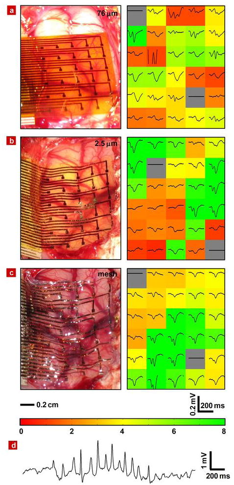
Image of electrode array on feline brain (left) and average evoked response from each electrode (right) with the color showing the ratio of the RMS amplitude of each average electrode response in the 200 ms window (plotted) immediately after the presentation of the visual stimulus to the RMS amplitude of the average 1.5 second window (not shown) immediately preceding the stimulus presentation for 76 μm a, 2.5 μm b and 2.5 μm mesh c electrode array. The stimulus presentation occurs at the left edge of the plotted window. In all 3 images, the occipital pole is at the bottom of the frame and medial is at the right. The scale bars at the bottom of c indicate the spatial scale for the left frames and the voltage and time scales for the right frames of a,b and c. The color bar at the bottom of c provides the scale utilized in the right frames of a,b, and c to indicate the RMS amplitude ratios. d, Representative voltage data from a single electrode in a 2.5 μm mesh electrode array showing a sleep spindle.
Three kinds of electrode arrays were used for comparison: 76 μm and 2.5 μm thick sheets and a 2.5 μm thick mesh. The second two included dissolvable silk supports. The left images of Fig 5a, b and c illustrate the progressively improved conformal contact with reduced thickness (i.e. 76 μm to 2.5 μm, in Fig. 5a and b, respectively) and with introduction of the mesh (i.e. Fig. 5c). The right frames of Fig 5a, b and c demonstrate the effectiveness of decreasing the electrode thickness and the mesh structure on physiological measurements of brain activity.
In particular, these frames show the average evoked response measured at each electrode, each plotted in a spatial arrangement that corresponds to the images in the left frames. Prominent visually evoked potentials are observed, particularly a strong P100 response. The P100 response is a “positive” evoked response typically occurring at 100 ms after the stimulation onset29. The P100 responses shown in Figure 5 appear in the negative direction because they have been plotted negative down as opposed to the neuroscience convention of plotting negative up. The background color of each plot illustrates a quantitative measure of the evoked response signal quality. This measure of signal quality was calculated by dividing the root mean square (RMS) amplitude of each average electrode response in the 200 ms window immediately after the presentation of the visual stimulus by the RMS amplitude of the average 1.5 second window immediately preceding the stimulus presentation. The color bar at the bottom of Fig. 5c provides the numerical scale for all of the colors used in Fig 5a, b and c. This measurement serves as a quantitative metric of the electrode performance, because the uniform nature of the stimulation is expected to evoke similar responses across the entire visual cortex.
In each case, 28 of the 30 electrode channels were recorded and evaluated for evoked potential response, as colored in green through red. Two channels, indicated in grey, were reserved as local references, as required by the recording apparatus, and were not evaluated. The channels with high and low RMS amplitude ratios are colored green and red, respectively. The 76 μm (Fig 5a) electrode array exhibited the lowest performance with a mean RMS amplitude ratio of all 28 channels of 3.6 ± 1.8. This was due to poor contact at many of the electrodes. The 2.5 μm array (Fig 5b) showed better conformal contact and correspondingly a higher mean RMS amplitude ratio of 5.2 ± 3.9. However the higher standard deviation and correspondingly wide spectrum of red and green channels on the array indicate that while many electrodes recorded excellent signals, approximately half of the electrodes still had poor contact with the brain and recorded weak responses. The 2.5 μm mesh electrode (Fig 5c) showed the best performance, with nearly all channels in good contact and a still higher mean RMS amplitude ratio of 5.7 ± 3.0. The lower standard deviation the 2.5 μm array illustrates that the majority of the electrodes recorded good responses.
Figure 5d shows representative single channel data from one of the 2.5 μm mesh electrodes. A sleep spindle is observed with good signal amplitude and signal to noise ratio. This collective set of observations is consistent with the systematic mechanics studies described previously. We did not observe any evidence of immune response. Histology data from related types of devices implanted under the skin exhibited no inflammation after 4 weeks, as shown in Fig. S10.
Although purely passive electrode systems serve to demonstrate the advantages and underlying aspects of these systems, the same approaches are compatible with fully active electronics and optoelectronics. This technology allows intimate integration of finely spaced electrode systems with living tissue, enabling the kind of reliable biotic/abiotic interface with moving, biological structures that will be required for chronically implanted, high resolution medical devices. This improved electrode-tissue interface has the potential for positive impact on human health in many modes of use.
METHODS
THICK ELECTRODE ARRAY (> 25 μM) FABRICATION
Commercial PI films (Kapton, Dupont, USA) with thicknesses of 25 and 75 μm were attached to a temporary carrier substrate consisting of a glass slide coated with PDMS. After cleaning the surfaces with acetone, isopropyl alcohol (IPA) and deionized (DI) water, electron beam evaporation formed uniform coatings of metal (Cr/Au, 50/1450 A). Photolithography and patterned etching yielded arrays of interconnect lines. Thin layers of PI (thickness ~1.2 μm) spin cast and patterned by reactive ion etching left only the ends of the lines exposed. Additional deposition and patterning defined square metal electrode pads at these locations. Peeling away from the PDMS coated glass slide and bonding to on ACF cable, using procedures described in a separate section, completed the fabrication. Figure S1 provides a schematic diagram and images of the process.
THIN ELECTRODE ARRAY (< 10 μM) FABRICATION
The fabrication in this case used a carrier silicon wafer coated with a thin (~1.2 μm) spin cast layer of poly(methylmethacrylate) (PMMA, A2, MicroChem, USA). The device substrate consisted of a film of PI (Sigma Aldrich, USA) spin cast onto the PMMA. Procedures similar to those described for thick devices formed the metal electrodes and PI overcoat. After fabrication, the ultrathin devices were released by dissolving the sacrificial PMMA layer. Transfer printing with a PDMS stamp delivered the devices to dry silk film substrates, coated with ~9% silk solution as an adhesive. The final step involved bonding of an ACF cable.
MESH ELECTRODE ARRAY (< 10 μM) FABRICATION
The first and last parts of the fabrication sequence were identical to the steps outlined in the previous section. The only difference was the addition of a step to remove certain regions of the polymer layers (i.e. PI and underlying PMMA) by oxygen reactive ion etching through a mask (design in Fig. S3) to define the mesh structure. Detailed dimensions are as follows: thickness ~2.5 μm, contact electrode size 500 μm × 500 μm, mesh width ~250 μm. (See more details in Fig. S5) This etching immediately followed the formation of the electrode pads.
ACF CONNECTION
The contact pads on the electrode array were first aligned with the ACF cable. Metal clips were used to apply pressure, spread evenly over the contact pad area using a piece of PDMS inserted between the ACF and the clips. Next, the clamped sample and ACF were placed in an oven preheated to ~150°C for ~15 min. This process formed a strong mechanical bond between the electrode array and the ACF with low electrical resistance.
DATA ACQUISITION AND PROCESSING
The electrode arrays were connected to a Neuralynx DigitalLynx data acquisition system via anisotropic conductive film (ACF) and a custom electrode interface board. The board appears in Fig. S11. Fig. S2 shows the connected electrode array, ACF ribbon and circuit board. The signals were sampled at the standard DigitalLynx sampling rate of 32556 Hz per channel. The high pass filter was set at 1 Hz and low pass filter at 9 kHz. Custom MATLAB software (The MathWorksTM, Natick, MA) was used for offline processing. Signals were down sampled to 2713 Hz and further low pass filtered at 50 Hz. Responses were averaged for each stimulus and plotted per electrode.
ANIMAL EXPERIMENTS
Experiments were conducted in accordance with the ethical guidelines of the National Institutes of Health and with the approval of the Institutional Animal Care and Use Committee of the University of Pennsylvania. Surgical and stimulation methods were as described in detail previously29, 30. Briefly, adult cats (2.5–3.5 kg) were anesthetized with intravenous thiopental with a continuous infusion (3–10 mg/kg/hr) and paralyzed with gallamine triethiodide (Flaxedil). Heart rate, blood pressure, end-tidal CO2 and EEG were monitored throughout the experiment to assure depth and stability of anesthesia and rectal temperature was kept at 37–38°C with a heating pad. The surface of the visual cortex was exposed with a craniotomy centered at Horsley Clarke posterior 4.0, lateral 2.0.
For visual stimulation, the corneas were protected with contact lenses after dilating the pupils with 1% ophthalmic atropine and retracting the nictitating membranes with phenylephrine (Neosynephrine). Spectacle lenses were chosen by the tapetal reflection technique to optimize the focus of stimuli on the retina. The position of the monitor was adjusted with an x-y-stage so that the area centralae were centered on the screen. Stimuli were presented on an Image Systems (Minnetonka, MN) model M09LV monochrome monitor operating at 125 frames per second at a spatial resolution of 1024 × 786 pixels and a mean luminance of 47 cd/m2.
Supplementary Material
Acknowledgments
We thank T. Banks and J.A.N.T. Soares for help using facilities at the Frederick Seitz Materials Research Laboratory. This material is based upon work supported by a National Security Science and Engineering Faculty Fellowship and the U.S. Department of Energy, Division of Materials Sciences under Award No. DEFG02-91ER45439, through the Frederick Seitz MRL and Center for Microanalysis of Materials at the University of Illinois at Urbana-Champaign. The aspects of the work relating to silk are supported by the U.S. Army Research Laboratory and the U.S. Army Research Office under contract number W911 NF-07-1-0618 and by the DARPA-DSO and the NIH P41 Tissue Engineering Resource Center (P41 EB002520). Work at the University of Pennsylvania is supported by the National Institutes of Health Grants (NINDS RO1-NS041811-04, R01 NS 48598-04), and the Klingenstein Foundation. One of the authors (JAR) is supported by a National Science Security and Engineering Faculty Fellowship.
Footnotes
Author Contributions
D.H.K., J.V., J.J.A., J.X., L.V., Y.S.K., D.C., D.L.K., F.G.O., Y.H, K.C.H., M.R.Z., B.L. and J.A.R. designed the experiments. D.H.K., E.S.F., J.V, J.J.A., J.X, L.V., Y.S.K. B. P. and J.A.B. performed experiments and analysis. D.H.K., J.V., J.J.A., J.X., L.V., J.A.B., D.C., D.L.K., F.G.O., Y.H, B.L. and J.A.R. wrote the paper.
Competing Financial Interests
The authors declare no competing financial interest.
Additional Information
Supplementary information accompanies this paper on www.Nature.com/naturematerials. Reprints and permissions information is available online at http://npg.nature.com/reprintsandpermissions.
References
- 1.Kim S, et al. Integrated wireless neural interface based on the Utah electrode array. Biomed Microdevices. 2009;11:453–466. doi: 10.1007/s10544-008-9251-y. [DOI] [PubMed] [Google Scholar]
- 2.Ryu SI, Shenoy KV. Human cortical prostheses: lost in translation? Neurosurg Focus. 2009;27(1):E5. doi: 10.3171/2009.4.FOCUS0987. [DOI] [PMC free article] [PubMed] [Google Scholar]
- 3.Andersen RA, Musallam S, Pesaran B. Selecting the signals for a brain–machine interface. Current Opinion in Neurobiology. 2004;14:720–726. doi: 10.1016/j.conb.2004.10.005. [DOI] [PubMed] [Google Scholar]
- 4.Mehring C, et al. Inference of hand movements from local field potentials in monkey motor cortex. Nature Neurosci. 2003;6:1253–1254. doi: 10.1038/nn1158. [DOI] [PubMed] [Google Scholar]
- 5.Ball T, et al. Towards an implantable brain-machine interface based on epicortical field potentials. Biomed Tech. 2004;49:756–759. [Google Scholar]
- 6.Wilson JA, Felton EA, Garell PC, Schalk G, Williams JC. ECoG factors underlying multimodal control of a brain–computer interface. IEEE Trans Neural Syst Rehabil Eng. 2006;14:246–250. doi: 10.1109/TNSRE.2006.875570. [DOI] [PubMed] [Google Scholar]
- 7.Freeman WJ, Rogers LJ, Holmes MD, Silbergeld DL. Spatial spectral analysis of human electrocorticograms including the alpha and gamma bands. J Neurosci Methods. 2000;95:111–121. doi: 10.1016/s0165-0270(99)00160-0. [DOI] [PubMed] [Google Scholar]
- 8.Kellis SS, House PA, Thomson KE, Brown R, Greger B. Human neocortical electrical activity recorded on nonpenetrating microwire arrays: applicability for neuroprostheses. Neurosurg Focus. 2009;27(1):E9. doi: 10.3171/2009.4.FOCUS0974. [DOI] [PMC free article] [PubMed] [Google Scholar]
- 9.Rubehn B, Bosman C, Oostenveld R, Fries P, Stieglitz T. A MEMS-based flexible multichannel ECoG-electrode array. J Neural Eng. 2009;6:036003. doi: 10.1088/1741-2560/6/3/036003. [DOI] [PubMed] [Google Scholar]
- 10.Hollenberg BA, Richards CD, Richards R, Bahr DF, Rector DM. A MEMS fabricated flexible electrode array for recording surface field potentials. J Neurosci Methods. 2006;153:147–153. doi: 10.1016/j.jneumeth.2005.10.016. [DOI] [PubMed] [Google Scholar]
- 11.Yu Z, Graudejus O, Tsay C, Lacour SP, Wagner S, Morrison B. Monitoring hippocampus electrical activity in vitro on an elastically deformable microelectrode array. J Neurotrauma. 2009;26:1135–1145. doi: 10.1089/neu.2008.0810. [DOI] [PMC free article] [PubMed] [Google Scholar]
- 12.Meacham KW, Giuly RJ, Guo L, Hochman S, DeWeerth SP. A lithographically-patterned, elastic multi-electrode array for surface stimulation of the spinal cord. Biomed Microdev. 2008;10:259–269. doi: 10.1007/s10544-007-9132-9. [DOI] [PMC free article] [PubMed] [Google Scholar]
- 13.Lawrence BD, Cronin-Golomb M, Georgakoudi I, Kaplan DL, Omenetto FG. Bioactive silk protein biomaterial systems for optical devices. Biomacromolecules. 2008;9:1214–1220. doi: 10.1021/bm701235f. [DOI] [PubMed] [Google Scholar]
- 14.Omenetto FG, Kaplan DL. A new route for silk. Nature Photon. 2008;2:641–643. [Google Scholar]
- 15.Jin HJ, et al. Water-stable silk films with reduced β-sheet content. Adv Funct Mater. 2005;15:1241–1247. [Google Scholar]
- 16.Lu Q, et al. Water-insoluble silk films with silk i structure. Acta Biomater. 2009 doi: 10.1016/j.actbio.2009.10.041. In Press. [DOI] [PMC free article] [PubMed] [Google Scholar]
- 17.Jiang C, et al. Mechanical properties of robust ultrathin silk fibroin films. Adv Funct Mater. 2007;17:2229–2237. [Google Scholar]
- 18.Sofia S, McCarthy MB, Gronowicz G, Kaplan DL. Functionalized silk-based biomaterials for bone formation. J Biomed Mater Res. 2001;54:139–148. doi: 10.1002/1097-4636(200101)54:1<139::aid-jbm17>3.0.co;2-7. [DOI] [PubMed] [Google Scholar]
- 19.Perry H, Gopinath A, Kaplan DL, Negro LD, Omenetto FG. Nano- and micropatterning of optically transparent, mechanically robust, biocompatible silk fibroin films. Adv Mater. 2008;20:3070–3072. [Google Scholar]
- 20.Murphy AR, John PS, Kaplan DL. Modification of silk fibroin using diazonium coupling chemistry and the effects on hMSC proliferation and differentiation. Biomaterials. 2008;29:2829–2838. doi: 10.1016/j.biomaterials.2008.03.039. [DOI] [PMC free article] [PubMed] [Google Scholar]
- 21.Altman GH, et al. Silk-based biomaterials. Biomaterials. 2003;24:401–416. doi: 10.1016/s0142-9612(02)00353-8. [DOI] [PubMed] [Google Scholar]
- 22.Santin M, Motta A, Freddi G, Cannas M. In vitro evaluation of the inflammatory potential of the silk fibroin. J Biomed Mater Res. 1999;46:382–389. doi: 10.1002/(sici)1097-4636(19990905)46:3<382::aid-jbm11>3.0.co;2-r. [DOI] [PubMed] [Google Scholar]
- 23.Kim DH, et al. Silicon electronics on silk as a path to bioresorbable, implantable devices. Appl Phys Lett. 2009;95:133701–133703. doi: 10.1063/1.3238552. [DOI] [PMC free article] [PubMed] [Google Scholar]
- 24.Amsden JJ, et al. Spectral analysis of induced color change on periodically nanopatterned silk films. Opt Express. 2009;17:21271–21279. doi: 10.1364/OE.17.021271. [DOI] [PubMed] [Google Scholar]
- 25.Parker ST, et al. Biocompatible silk printed optical waveguides. Adv Mater. 2009;21:2411–2415. [Google Scholar]
- 26.Soong HK, Kenyon KR. Adverse reactions to virgin silk sutures in cataract surgery. Ophthalmology. 1984;91:479–483. doi: 10.1016/s0161-6420(84)34273-7. [DOI] [PubMed] [Google Scholar]
- 27.Chaudhury MK, Whitesides GM. Direct measurement of interfacial interactions between semispherical lenses and flat sheets of poly(dimethylsiloxane) and their chemical derivatives. Langmuir. 1991;7:1013–1025. [Google Scholar]
- 28.Someya T, et al. Conformable, flexible, large-area networks of pressure and thermal sensors with organic transistor active matrixes. Proc Natl Acad Sci USA. 2005;102:12321–12325. doi: 10.1073/pnas.0502392102. [DOI] [PMC free article] [PubMed] [Google Scholar]
- 29.Padnick LB, Linsenmeier RA. Properties of the flash visual evoked potential recorded in the cat primary visual cortex. Vision Research. 1999;39:2833–2840. doi: 10.1016/s0042-6989(99)00016-4. [DOI] [PubMed] [Google Scholar]
- 30.Cardin JA, Palmer LA, Contreras D. Stimulus Feature Selectivity in Excitatory and Inhibitory Neurons in Primary Visual Cortex. J Neurosci. 2007;27:10333–10344. doi: 10.1523/JNEUROSCI.1692-07.2007. [DOI] [PMC free article] [PubMed] [Google Scholar]
- 31.Cardin JA, Palmer LA, Contreras D. Cellular Mechanisms Underlying Stimulus-Dependent Gain Modulation in Primary Visual Cortex Neurons In Vivo. Neuron. 2008;59:150–160. doi: 10.1016/j.neuron.2008.05.002. [DOI] [PMC free article] [PubMed] [Google Scholar]
Associated Data
This section collects any data citations, data availability statements, or supplementary materials included in this article.