Abstract
Lead-free K0.5Na0.5NbO3/Bi0.5Na0.5TiO3 (KNN/BNT) films have been fabricated by a composite sol-gel technique. Crystalline KNN fine powder was dispersed in the BNT precursor solution to form a composite slurry which was then spin-coated onto a platinum-buffered Si substrate. Repeated layering and vacuum infiltration were applied to produce 5-μm-thick dense composite film. By optimizing the sintering temperature, the films exhibited good dielectric and ferroelectric properties comparable to PZT films. A 193-MHz high-frequency ultrasonic transducer fabricated from this composite film showed a −6-dB bandwidth of approximately 34%. A tungsten wire phantom was imaged to demonstrate the capability of the transducer.
I. Introduction
Ferroelectric materials such as lead zirconate titanate (PZT) have been widely used for piezoelectric device applications such as actuators and ultrasonic transducers. In the field of medical imaging, the market share of ultrasound imaging is expected to gradually increase because its resolution and cost-effectiveness compare favorably with X-ray, CT, and magnetic resonance imaging. High-frequency ultrasound has many clinical applications including visualizing blood vessel walls, anterior segments of the eye, and skin [1]–[3]. In response to the need for increased resolution, much effort has been made toward the development of medical ultrasonic transducers with operating frequency greater than 100 MHz; because the piezoelectric films have to be made with thickness less than 20 μm, this remains a challenge following more than a decade of study [4]–[8].
In recent years, several processes such as aerosol deposition [9], [10], screen-printing [11], composite sol-gel [12], [13], and ink-jet printing [14] have been studied to reach this thickness range without compromising the piezoelectric properties in comparison to those of bulk materials. Among these techniques, the composite sol-gel process first developed by Barrow et al. [15] has received much attention because this method not only possesses the advantages of sol-gel method, i.e., good control of film stoichiometry, low production cost, and low annealing temperature, but can also produce thick layers in the range of 1 to 50 μm without cracks by adding ceramic powder to reduce the stress within the composite thick film. Several researchers have successfully fabricated dense and crack-free PZT composite thick films for high-frequency ultrasound transducer applications [16]–[18]. Although PZT with composition close to morphotropic phase boundary (MPB) offers very strong piezoelectric activity, the use of this lead-based material has caused serious environmental problems.
Currently, extensive research studies on lead-free systems with a perovskite-type structure, such as (K0.5Na0.5) NbO3 (KNN)-based and bismuth sodium titanate (Bi0.5Na0.5)TiO3 (BNT)-based ceramics have produced much progress. The KNN-based ceramics exhibit a high Curie temperature Tc (above 400°C) and large electromechanical coupling factors (k33 = 0.51 to 0.6, kp = 0.35 to 0.50) [19]. The BNT family shows strong ferroelectricity with a relatively large remnant polarization of ~38 μC/cm2 [20]. Thus, both materials are promising candidates for actuator and high-power applications, and also for medical ultrasonic imaging applications. Recently, lead-free KNN 0–3 composite using KNN fine powder dispersed in a sol-gel precursor solution has been considered for high-frequency transducer application. However, the high cost of the KNN precursor solution prepared from expensive niobium ethoxide may limit the applications of the KNN thick film. Thus, BNT precursor solution, with its good ferroelectric properties and low cost, can be an alternative for use as the matrix of the composite film. The electrical properties of KNN/BNT thick films derived by composite sol-gel technique and their performance for use as ultrasound devices are rarely reported.
In this work, we combine these two lead-free ceramics by blending the fine crystalline KNN powder into the BNT precursor solution to form a homogeneous 0–3 composite slurry, followed by spin-coating. To improve the film density, vacuum filtration is used during the deposition process. The thermal treatment has been optimized to achieve better dielectric and ferroelectric properties of the film. The performance of a high-frequency ultrasonic transducer fabricated with this lead-free film was also demonstrated.
II. Experimental
A. Fabrication and Characterization of KNN/BNT Thick Film
Reagent-grade raw materials of K2CO3 (99%), Na2CO3 (99.8%) and Nb2O5 (99.5%) were used to prepare the KNN powder by a conventional solid-state reaction method. The raw powder mixture was ball-milled in anhydrous ethanol at 400 rpm for 4 h, and pressed into disks for calcination at 1000°C for 4 h. To obtain fine KNN powder, the calcined ceramic blocks were crushed and ball-milled at 400 rpm for 7 h. The precursor solution of BNT was synthesized by sol-gel process using bismuth nitrate pentahydrate, tetrabutyl titanate, and sodium acetate as the raw materials, 2-methoxyethanol as the solvent, and acetylaceton as the chelating agent. To compensate for the loss of Na and Bi during thermal treatment, an excess amount of 10 mol% sodium acetate and 2 mol% bismuth nitrate pentahydrate were introduced. In this work, the composite slurry was prepared by mixing BNT solution of 0.45 M in concentration and KNN powder with the powder-to-solution ratio of 0.4 (wt%). The KNN/BNT composite films were deposited on (111) Pt/TiO2/SiO2/Si substrate by spin coating. A two-stage pyrolysis sequence, consisting of a 3 min heat treatment at 150°C followed by another at 410°C for 10 min, was applied in a rapid thermal process furnace to drive out the solvent and decompose the organic compounds. To increase the film crystallinity, the composite films were annealed at greater than 650°C for 3 min. In this work, three annealing temperatures (650, 700, and 750°C) were used to investigate the effect of the annealing temperature on the film properties. To improve the film density, a vacuum infiltration process [21] with BNT precursor solution was applied after each coating of the KNN/BNT composite film. This procedure was repeated until film thickness of ~5 μm was achieved.
The particle size distribution of the KNN powder was measured by a BT-9300H laser particle size analyzer (BT-9300H, Bettersize Instruments Ltd, China). The crystallographic properties of KNN/BNT composite films were analyzed by X-ray diffractometry (XRD). The morphology of the composite films was observed by field emission scanning electron microscopy (FE-SEM). The chromium/gold (Cr/Au) electrode with dimension of 0.5 × 0.5 mm2 was deposited on the top surface of the annealed film by sputtering at room temperature. The dielectric properties were measured using an Agilent 4294A impedance analyzer (Agilent Technologies, Santa Clara, CA). The polarization-electric field hysteresis loop of the composite films was measured by a modified Sawyer-Tower circuit. All measurements were conducted at room temperature.
B. Fabrication and Evaluation of Transducer
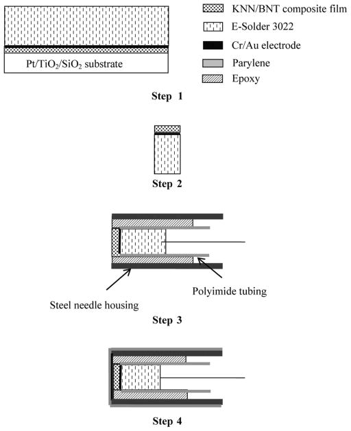
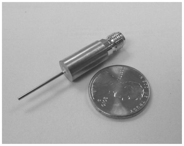
KNN/BNT thick film transducers were built using a silicon etching process [22] and conventional transducer technology [5]. Fig. 1 shows the fabrication procedure for the high-frequency needle transducer with the composite film as active element. First, a very lossy conductive epoxy (E-Solder 3022, Von Roll Isola Inc., New Haven, CT) with an acoustic impedance of ~6 MRayl was applied to the film as the backing material by centrifuged casting. After curing at room temperature overnight, the backing layer was lapped down to 1 mm thick. The sample was then diced along the thickness direction into small posts with dimensions of 0.25 × 0.25 mm. The film with the support of the backing layer was removed from the Si substrate without any damage by wet etching the substrate in 20% concentrated KOH solution at 80°C for 5 to 10 min. A lead wire with a diameter of 0.1 mm was connected to the backing layer using conductive epoxy. The KNN/BNT element was fixed into a steel needle housing using epoxy. After the epoxy had set, a Cr/Au layer was sputtered across the active element and the needle housing to serve as the grounding. A 1.5-μm-thick parylene layer was vapor-deposited on the front face of the transducer to serve as an acoustic matching layer and also as a protection layer. The final transducer was housed in an SMA connector as shown in Fig. 2 for poling and pulse-echo measurement. To induce the piezoelectric response of the composite element, the sample was heated to 115°C and an electric field of 210 kV/cm (about two times the coercive field) was applied for 10 min.
Fig. 1.
Fabrication process for the needle transducer. Step 1: A Cr/Au electrode was sputtered on the KNN/BNT composite film and a conductive epoxy (E-Solder 3022) was cast on the electrode side as the backing. Step 2: The sample was diced into 0.25 × 0.25 mm posts and the substrate was removed by dipping in KOH solution at 80°C. Step 3: A lead wire was connected to the backing layer using conductive epoxy. The element was inserted into a polyimide tube and was then fixed into the housing of a steel needle using epoxy. Step 4: A Cr/Au electrode was sputtered across the KNN/BNT composite element and needle housing to form the ground plane connection. Vapor-deposited parylene (1.5 μm thick) was used to coat the aperture and the needle housing. The finished transducer was housed in the SMA connector as shown in Fig. 2.
Fig. 2.
Photo of the KNN/BNT composite needle transducer.
The performance of the transducer was evaluated in deionized water by a pulse-echo arrangement [5]. The transducer was connected to a Panametrics model 5910R pulser/receiver (Panametrics NDT, Waltham, MA), and excited by an electrical impulse with 200 Hz repetition and 50 Ω damping. An X-cut quartz plate was used as a target. The testing distance is in the far-field region of the transducer. The reflected waveform was received and digitized by a 1-GHz LC534 LeCroy oscilloscope (LeCroy Corp., Chestnut Ridge, NY) with 50 Ω coupling. The math feature on the oscilloscope was used to display the fast Fourier transform (FFT) of the received waveform. The center frequency and the −6-dB bandwidth were determined from the measured frequency spectrum.
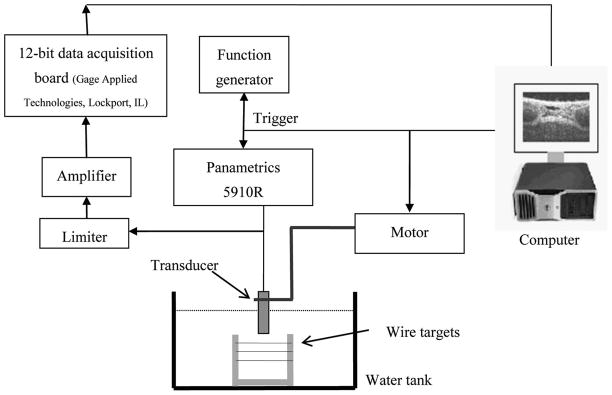
To assess the axial and lateral resolution of the transducer, a series of tungsten wires with diameter of 6 μm (California Fine Wire Co., Grover Beach, CA) was imaged using the pulse-echo setup described previously. The experimental setup is schematically illustrated in Fig 3. The remote amplifier portion of the Panamatrics 5910R set at 30.5 dB gain was used along with 12-bit data acquisition board (Gage Applied Technologies, Lockport, IL) working at the sampling rate of 400 MHz. Piezoelectric actuators (Inchworm, Burleigh Inc., Fishers, NY) were used to scan the wire across the transducer sound field with a step size of 2 μm. The amplified RF waveforms were acquired at each step by the LC534 and then used to form an image offline. The −6-dB resolutions of the transducer were then measured from the axial and lateral line spread functions for the recorded wire image.
Fig. 3.
Schematic diagram of the experimental setup for the imaging of the wire phantom.
III. Results and Discussion
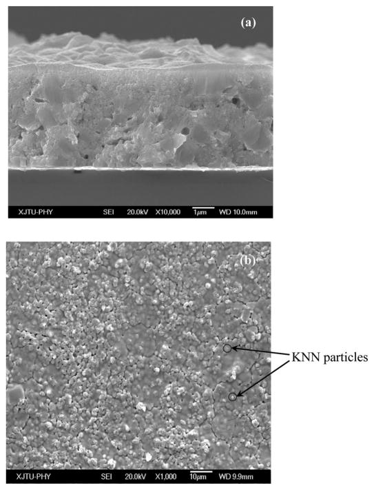
Fig. 4 shows the XRD patterns of the KNN/BNT composite films annealed at three different temperatures (650, 700, and 750°C). All films exhibit composite perovskite phases with KNN and BNT phases. The increase in the intensities of the XRD peaks with the annealing temperature reveals that the crystallinity of the composite film can be enhanced by proper thermal treatment. The cross-sectional and surface FE-SEM images of the KNN/BNT films annealed at 750°C are shown in Figs. 5(a) and 5(b), respectively. The film thickness is ~5 μm. As shown in Fig. 5(b), KNN particles with large grain size of ~1 μm are embedded evenly in the BNT matrix to form a 0–3 composite film. The particle size distribution analysis for the KNN powder indicates that the median particle size d50 is 0.92 μm; the larger particles d97 and smaller particles d03 are 1.23 μm and 0.64 μm, respectively, which is in agreement with the FE-SEM observation. A riverbed cracking is observed which is caused by vertical cracks. Excessive cracking may lead to electrical and mechanical isolation in the areas of the film, resulting in poor performance. Generally, such cracking arises as the film thickness increases because the ceramic particles within the gel are no longer able to move to accommodate shrinkage induced by the removal of organic solvent. This causes the internal tensile stress to increase until the bonding between the individual particles is disrupted. Because this composite film exhibits good dielectric and ferroelectric properties, as discussed in detail below, the low degree of cracking achieved in these films indicates that the two-stage pyrolysis sequence enables good rearrangement of the ceramic particles.
Fig. 4.
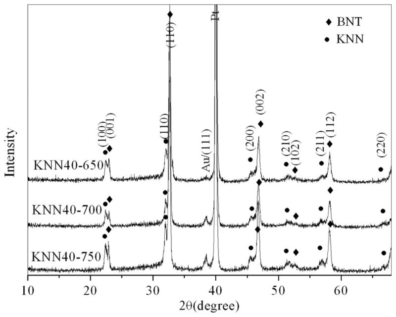
X-ray diffreactometry pattern of KNN/BNT composite film films annealed at different temperatures.
Fig. 5.
(a) Cross-sectional (fracture surface) and (b) surface images of the KNN/BNT composite film annealed at 750°C.
The ferroelectric hysteresis loops of the composite films with different annealing temperatures were measured and the results are presented in Fig. 6. Saturated hysteresis loops are observed when the electric field is increased to ~800 kV/cm. By increasing the annealing temperature, both remnant polarization Pr and coercive field Ec increase because of the improvement of the film crystallinity, as confirmed by the XRD analysis. Based on our preliminary study, similar results were observed in pure BNT thick films. The dielectric constant and dielectric loss of the composite films were also measured by an impedance analyzer. Table I summarizes the ferroelectric and dielectric properties of the composite films annealed at different temperatures. For comparison, pure BNT film annealed at 750°C was also prepared and its properties were measured. The performances of pure KNN film and PZT 0–3 composite sol-gel films reported in the literature [12], [13], [22], [23] were also included. It can be seen that ferroelectric and dielectric properties can be improved by annealing the composite film up to 750°C. In comparison with pure KNN film and BNT film, the KNN/BNT composite film shows intermediate ferroelectric properties. The KNN/BNT film has dielectric constant of ~850 and remnant polarization of ~24 μC/cm2, comparable to those of PZT films reported in the literature. These properties indicate that this lead-free material may be attractive for piezoelectric device applications.
Fig. 6.
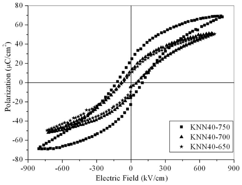
Polarization-electric field hysteresis loops of KNN/BNT composite films annealed at different temperatures.
TABLE I.
Ferroelectric and Dielectric Properties of the Composite Films Annealed at Different Temperatures.
| Sample | Measured property |
|||
|---|---|---|---|---|
| Pr (μC/cm2) | Ec (kV/cm) | εr at 1 kHz | tan δ at 1 kHz | |
| KNN/BNT (650°C) | 10.1 | 68 | 698 | 0.031 |
| KNN/BNT (700°C) | 12.8 | 71 | 733 | 0.028 |
| KNN/BNT (750°C) | 23.6 | 108 | 848 | 0.029 |
| BNT (750°C) | 34.2 | 143 | 900 | 0.033 |
| KNN [23] | 16.4 | 42 | — | — |
| Soft doped PZT [12] | 15 | 23 | 900 | — |
| PZT 52/48 [13], [22] | 16–37 | 40–43 | 680–1250 | 0.040 |
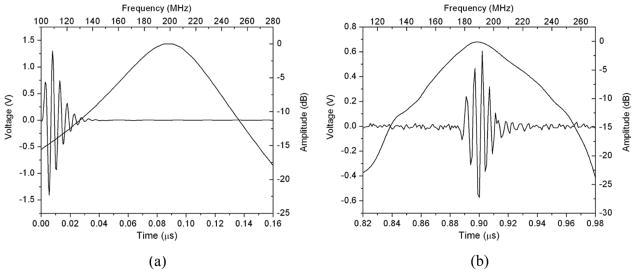
Fig. 7(a) shows the modeled result of the KNN/BNT composite transducer with Krimholtz, Leadom and Met-taei (KLM)-model-based stimulation software PIEZO-CAD (Sonic Concepts, Woodinville, WA). The modeled center frequency and −6-dB bandwidth are 195 MHz and 38%, respectively. Fig. 7(b) shows the measured pulse-echo waveform and frequency spectrum of the KNN/BNT thick film transducer. The center frequency of the composite transducer are 193 MHz, and the −6-dB bandwidth was 65 MHz (fractional bandwidth ~34%), which are in agreement with the modeled data. To measure the axial and lateral resolution of the transducer, a series of tungsten wires with a diameter of 6 μm was imaged and the result are presented in Fig. 8. The measured −6-dB resolutions estimated from the point spread function of the target image (located 1.25 mm from the transducer) are 18 μm in the axial direction and 48 μm in the lateral direction. With this high spatial resolution, the composite transducer is capable of examining biological structures with resolution approaching several tens of micrometers. The results imply that this lead-free film is a promising material and may serve as an alternative to PZT films not only for high-frequency ultrasonic transducers but also for other micro-device applications.
Fig. 7.
(a) Modeled result of the composite transducer with KLM model-based simulation software PIEZOCAD. (b) Measured pulse-echo waveform and spectrum for the KNN/BNT needle transducer.
Fig. 8.
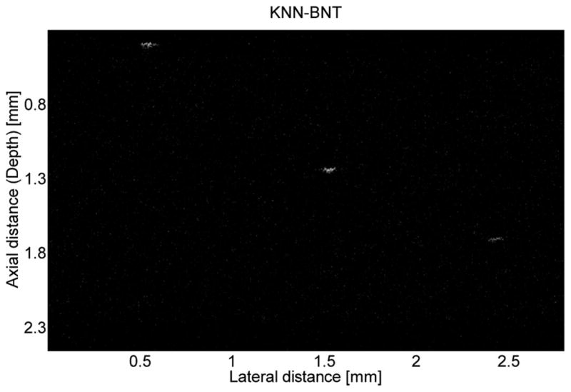
Wire target image acquired with the KNN/BNT needle transducer.
IV. Conclusions
Lead-free KNN/BNT films with a thickness of ~5 μm have been successfully fabricated on a platinum-buffered Si substrate using a modified 0–3 composite sol-gel method. By optimizing the annealing temperature, the KNN/BNT film exhibits good dielectric and ferroelectric properties with dielectric constant of ~850 and remnant polarization of ~24 μC/cm2. Using this KNN/BNT film as the active element, a 193-MHz high-frequency ultrasonic transducer with good spatial resolution has been demonstrated. Experimental results imply that this lead-free film is a promising candidate as an alternative to PZT films for piezoelectric device applications.
Acknowledgments
This work was financially supported by NIH Grant P41-EB2182, the State Key Development Program for Basic Research of China (Grant No. 2008CB617610), and the Shaanxi Province International Collaboration Program (Grant No. 2010KW-09).
Contributor Information
Sien Ting Lau, Email: sienlau@usc.edu, Department of Biomedical Engineering and NIH Transducer Resource Center, University of Southern California, Los Angeles, CA.
Hong Fen Ji, Electronic Materials Research Laboratory, Key Laboratory of the Ministry of Education, Xi’an Jiantong University, Xi’an, China.
Xiang Li, Department of Biomedical Engineering and NIH Transducer Resource Center, University of Southern California, Los Angeles, CA.
Wei Ren, Electronic Materials Research Laboratory, Key Laboratory of the Ministry of Education, Xi’an Jiantong University, Xi’an, China.
Qifa Zhou, Department of Biomedical Engineering and NIH Transducer Resource Center, University of Southern California, Los Angeles, CA.
K. Kirk Shung, Department of Biomedical Engineering and NIH Transducer Resource Center, University of Southern California, Los Angeles, CA.
References
- 1.Turnbull DH, Starkoski BG, Harasiewicz KA, Semple JL, From L, Gupta AK, Sauder DN, Foster FS. A 40–100 MHz B-scan ultrasound backscatter microscope for skin imaging. Ultrasound Med Biol. 1995;21(1):79–88. doi: 10.1016/0301-5629(94)00083-2. [DOI] [PubMed] [Google Scholar]
- 2.Shung KK, Zipparo M. Ultrasonic transducers and arrays. IEEE Eng Med Biol Mag. 1996;15(6):20–30. [Google Scholar]
- 3.Coleman DJ, Silverman RJ, Chabi A, Rondeau MJ, Shung KK, Cannata J, Lincoff H. High-resolution ultrasonic imaging of the posterior segment. Ophthalmology. 2004;111(7):1344–1351. doi: 10.1016/j.ophtha.2003.10.029. [DOI] [PubMed] [Google Scholar]
- 4.Liu R, Harasiewicz KA, Foster FS. Interdigital pair bonding for high frequency (20–50 MHz) ultrasonic composite transducers. IEEE Trans Ultrason Ferroelectr Freq Control. 2001;48(1):299–306. doi: 10.1109/58.896143. [DOI] [PubMed] [Google Scholar]
- 5.Cannata JM, Ritter TA, Chen WH, Silverman RH, Shung KK. Design of efficient, broadband single-element (20–80 MHz) ultrasonic transducers for medical imaging applications. IEEE Trans Ultrason Ferroelectr Freq Control. 2003;50(11):1548–1557. doi: 10.1109/tuffc.2003.1251138. [DOI] [PubMed] [Google Scholar]
- 6.Marechal P, Levassort F, Holc J, Tran-Huu-Hue L-P, Kosec M, Lethiecq M. High-frequency transducers based on integrated piezoelectric thick films for medical imaging. IEEE Trans Ultrason Ferroelectr Freq Control. 2006;53(8):1524–1533. doi: 10.1109/tuffc.2006.1665110. [DOI] [PubMed] [Google Scholar]
- 7.Zhu BP, Wu DW, Zhou QF, Shi J, Shung KK. Lead zirconate titanate thick film with enhanced electrical properties for high frequency transducer applications. Appl Phys Lett. 2008;93(1) doi: 10.1063/1.3095504. art. no. 012905. [DOI] [PMC free article] [PubMed] [Google Scholar]
- 8.Lau ST, Zhao LB, Chan HLW, Luo HS. 60-MHz PMN-PT single crystal transducers for microfluidic analysis systems. Sens Actuators A. 2010;161(1–2):78–82. [Google Scholar]
- 9.Lebedev M, Akedo J. Effect of thickness on the piezoelectric properties of lead zirconate titanate films fabricated by aerosol deposition method. Jpn J Appl Phys. 2002;41(11b):6669–6673. [Google Scholar]
- 10.Choi JJ, Hahn BD, Ryu JH, Yoon WH, Park DS. Effects of Pb(Zn1/3Nb2/3)O3 addition and postannealing temperature on the electrical properties of Pb(ZrxTi1-x)O3 thick films prepared by aerosol deposition method. J Appl Phys. 2007;102(4) art. no. 044101. [Google Scholar]
- 11.Thiele ES, Damjanovic D, Setter N. Processing and properties of screen-printed lead zirconate titanate piezoelectric thick films on electroded silicon. J Am Ceram Soc. 2001;84(12):2863–2868. [Google Scholar]
- 12.Dorey RA, Whatmore RW. Electrical properties of high density PZT and PMN-PT/PZT thick films produced using ComFi technology. J Eur Ceram Soc. 2004;24(6):1091–1094. [Google Scholar]
- 13.Wu DW, Zhou QF, Shung KK, Bharadwaja SSN, Zhang DS, Zhang HJ. Dielectric and piezoelectric properties of PZT composite thick films with variable solution to powder ratios. J Am Ceram Soc. 2009;92(6):1276–1279. doi: 10.1111/j.1551-2916.2009.03065.x. [DOI] [PMC free article] [PubMed] [Google Scholar]
- 14.Wang TM, Derby B. Ink-jet printing and sintering of PZT. J Am Ceram Soc. 2005;88(8):2053–2058. [Google Scholar]
- 15.Barrow DA, Petroff TE, Sayer M. Thick ceramic coatings using a sol gel based ceramic-ceramic 0–3 composite. Surf Coat Tech. 1995;76(1–3):113–118. [Google Scholar]
- 16.Zhu H, Miao H, Wang ZH, Zhao CL, Zhu WG. Fabrication of ultrasonic arrays with 7 μm PZT thick films as ultrasonic emitter for object detection in air. Sens Actuators A. 2005;123–124:614–619. [Google Scholar]
- 17.Bardaine A, Boy P, Belleville P, Acher O, Levassort F. Improvement of composite sol-gel process for manufacturing 40 μm piezoelectric thick films. J Eur Ceram Soc. 2008;28(8):1649–1655. [Google Scholar]
- 18.Zhu BP, Wu DW, Zhou QF, Shi J, Shung KK. Lead zirconate titanate thick film with enhanced electrical properties for high frequency transducer applications. Appl Phys Lett. 2008;93(1) doi: 10.1063/1.3095504. art. no. 012905. [DOI] [PMC free article] [PubMed] [Google Scholar]
- 19.Shrout TR, Zhang SJ. Lead-free piezoelectric ceramics: Alternatives for PZT? J Electroceram. 2007;19(1):111–124. [Google Scholar]
- 20.Xiao DQ, Wu JG, Wu L, Zhu JG, Yu P, Lin DM, Liao YW, Sun Y. Investigation on the composition design and properties study of perovskite lead-free piezoelectric ceramics. J Mater Sci. 2009;44(19):5408–5419. [Google Scholar]
- 21.Dorey RA, Strinfellow SB, Whatmore RW. Effect of sintering aid and repeated sol infiltrations on the dielectric and piezoelectric properties of a PZT composite thick film. J Eur Ceram Soc. 2002;22(16):2921–2926. [Google Scholar]
- 22.Zhang QQ, Djuth FJ, Zhou QF, Hu C, Cha JH, Shung KK. High frequency broadband PZT thick film ultrasonic transducers for medical imaging applications. Ultrasonics. 2006;44(suppl 1):711–715. doi: 10.1016/j.ultras.2006.05.130. [DOI] [PubMed] [Google Scholar]
- 23.Wang LY, Yao K, Ren W. Piezoelectric K0.5Na0.5NbO3 thick films derived from polyvinylpyrrolidone-modified chemical solution deposition. Appl Phys Lett. 2008;93(9) art. no. 092903. [Google Scholar]


