Abstract
Micrometer-sized hollow antiresonant reflecting optical waveguides on silicon substrates have been previously demonstrated with liquid and gas-filled cores. Previous designs have nonideal geometries, with nonuniform lateral layers around the hollow core, resulting in higher loss than could potentially be achieved. A new design and fabrication process has been developed involving hollow waveguide fabrication on a self-aligned pedestal (SAP) using anisotropic plasma etching. With the SAP structure, the hollow core is surrounded by uniform layers and a terminal layer of air on three sides, resulting in air-core waveguide loss of 1.54 cm−1 at 785 nm and high fabrication yield.
Index Terms: Fabrication, optical waveguides, plasma materials-processing applications
I. Introduction
Hollow optical waveguides enable waveguiding in low-index media and direct light interaction with a variety of nonsolid media. Many applications in biology, chemistry, and atomic physics can benefit from this capability. Two methods of realizing hollow waveguides are commonly used: index guiding and interference guiding. As with traditional optical waveguides, index-guiding hollow waveguides rely on total internal reflection and require the cladding to have a lower refractive index than the core. Consequently, index-guiding hollow waveguides have been limited to liquid media (n ≈ 1.33) and use low-index cladding materials such as nanoporous films [1] or Teflon AF [2]. Interference-guiding allows for waveguiding in both gas and liquid-filled cores, relying on optical interference to confine light to the low-index core. Some types of hollow waveguides created using interference-guiding are photonic crystals [3], Bragg waveguides [4], and antiresonant reflecting optical waveguides (ARROWs) [5], [6].
ARROW waveguides rely on one or more antiresonant layers surrounding a guiding core [7]. The thickness of each layer is chosen such that the layer functions as a reflecting Fabry–Pérot etalon, allowing for low-loss optical guiding along the core. We have developed ARROW waveguides with micrometer-sized hollow cores and have integrated hollow and traditional solid waveguides to form sensor platforms. These platforms have been used for many applications with both liquid and air-filled cores, including optical trapping [8], virus detection [9], and on-chip Rubidium spectroscopy [10].
Our ARROW waveguides are fabricated on Si substrates and use standard processing techniques, including plasma-enhanced chemical vapor deposition (PECVD), contact lithography, and sacrificial etching. Hollow ARROWs demonstrated in the past were fabricated on planar [5] or pre-etched substrates [11], and structures were nonideal for lowest loss. In this letter, we present a new fabrication method for hollow-core ARROWs, using a self-aligned pedestal (SAP) to create near-ideal hollow-core geometries with lower waveguide loss and high fabrication yield.
II. Low-Loss ARROW Design
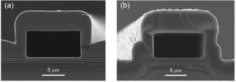
The first hollow ARROWs were fabricated on a planar substrate, as shown in Fig. 1(a). While ARROWs are inherently leaky waveguides, this design is particularly leaky because horizontal layers extend laterally from the hollow core. Light leaks out of the sides of the hollow core and into these horizontal cladding layers, resulting in high loss. Also, the PECVD layers do not uniformly coat the rectangular waveguide core, and the top of the core is coated more thickly than the sides. This leads to a shadowing effect for film deposition on the sides of the core, with the vertical cladding layers slightly thinner at the bottom than at the top. These nonuniform lateral layers also contribute to higher loss.
Fig. 1.

ARROW hollow waveguide designs: (a) First design on a planar substrate. (b) Second design on a pre-etched substrate. (Light gray: SiO2; dark gray: SiN).
One approach to increase light confinement and decrease loss in ARROWs is to surround the guiding core on three sides with a terminal layer of air [11]. To achieve this air-clad structure, we investigated a second ARROW design which consists of creating hollow waveguides on top of a pre-etched substrate, as depicted in Fig. 1(b). This air-clad structure increases light confinement in the core and results in lower loss than achieved with the first ARROW design. With this second design, it is necessary to create a pedestal on the substrate which is wider than the core to allow for alignment variations when the core is defined. In practice, any misalignment results in a noncentered core, which increases loss. The wider pedestal creates nonuniform layers on the sides of the core, which also increases loss. Another drawback with this structure is reduced fabrication yield, which occurs because of weakness in the films on the sides of the core where breakage can occur during sacrificial core removal.
Ideally, the hollow ARROW core would have uniform surrounding layers and a terminal layer of air on three sides. This third-generation ARROW design relies on an SAP to create the desired geometry. Since the width of the underlying pedestal is defined by the sacrificial core, no alignment step is necessary. The uniform layers on the sides of the core would reduce loss and increase the strength of the structure, resulting in higher yield.
III. Fabrication
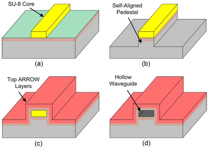
In order to fabricate SAP ARROWs, a process based on anisotropic plasma etching was chosen and is depicted in Fig. 2. The rest of the fabrication process is similar to that for ARROWs on planar substrates, based on PECVD and sacrificial etching [5]. First, layers of silicon dioxide (SiO2) and silicon nitride (SiN) are deposited by PECVD on a Si substrate at 250 °C [see Fig. 2(a)]. These layers are deposited with controlled refractive indexes and precise thicknesses so that each layer satisfies the antiresonant condition [7]. Next, the SU-8 sacrificial layer is deposited and patterned into the core shape by photolithography. After this, the SAP is created by anisotropic plasma etching, using a Minilock Phantom III Reactive Ion Etcher (RIE) with an inductively coupled plasma (ICP) RF generator (Trion Technology). Selective etching is required so that the SU-8 core is not removed while etching through 1–1.5 μm of PECVD SiO2 and SiN layers and 4–5 μm of the Si substrate to form the pedestal. We have developed separate etch recipes for etching the PECVD layers and the Si substrate, as shown in Table I. Etching of the PECVD layers is performed in a single etch step at an average rate of 170 nm/min. Etching of the Si substrate is performed with alternating sidewall passivation and etch steps, repeated many times, with an etch rate of about 18 nm/s.
Fig. 2.

Cross-sectional view of SAP ARROW fabrication: (a) Bottom PECVD antiresonant layers and sacrificial SU-8 core deposited. (b) SAP etched. (c) Top PECVD antiresonant layers deposited. (d) Sacrificial core exposed and removed in a piranha etch, completing the hollow waveguide.
Table I.
SAP Etching Recipes
| Recipe | ICP (W) | RIE (W) | Pressure (mTorr) | Gases (sccm) | ||
|---|---|---|---|---|---|---|
| CHF3 | O2 | SF6 | ||||
| SiO2 and SiN | 350 | 70 | 18 | 125 | 9 | 0 |
| Si Passivation | 550 | 0 | 120 | 75 | 0 | 0 |
| Si Etch | 550 | 60 | 35 | 30 | 0 | 20 |
| Isotropic Si Etch | 0 | 200 | 150 | 0 | 0 | 52 |
The CHF3 in the etching recipes provides sidewall passivation and increases the anisotropy of the etch. During etching, a fluorocarbon passivation film is deposited isotropically on the surface. Ion bombardment keeps horizontal surfaces clear of the film, while the film accumulates on and protects vertical surfaces. After etching is completed, the accumulated passivation film, commonly called post-etch residue, remains on the sides of the pedestal and the sacrificial core, and must be removed prior to deposition of the top antiresonant layers.
Various approaches have been used to remove this etch residue, including O2 and H2 plasmas, hydroxylamine, super-critical CO2 (SCCO2) [12], and radical anions [13]. We developed a cleaning procedure using a mixture of H2O2 and the resist remover RS-6 (Cyantek Corp.), which contains tetramethylammonium hydroxide (TMAH). To remove the etch residue, our samples are immersed in the mixture (1 : 10 50% H2O2 RS – 6) at 40 °C for 5 min and then rinsed in deionized water. This cleaning process is performed after the SiO2–SiN etch and again after the Si etching and effectively removes the etch residue without damaging the SU-8 core.
Another common problem encountered with anisotropic etching is the formation of etch grass. This occurs when surface defects and contamination function as micromasks and lead to the formation of small pillars, known as grass, on the etched surface. This issue can be particularly severe in our SAP etching, as the PECVD layers contain many defects which can function as micromasks [14]. To remove this etch grass, we employ an isotropic Si etch at the end of the pedestal etching. This etch attacks the sides of the grass and etches away the Si base to the point that the grass collapses, so it can be later rinsed away.
After the pedestal etching is completed and the etch residue and grass are removed, the top antiresonant layers are deposited by PECVD [see Fig. 2(c)]. Finally, the ends of the sacrificial core are exposed, either by cleaving the wafer or by plasma etching, and the core is removed in a piranha etch (1 : 1 50% H2O2 : 98% H2SO4, 100 °C), completing the hollow waveguide, as depicted in Fig. 2(d).
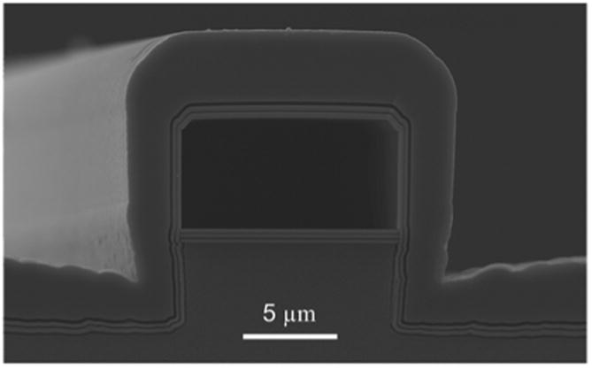
Fig. 3 shows an SEM image of a completed hollow SAP ARROW with nearly ideal geometry. Compared to the second ARROW design [see Fig. 1(b)], we see that the layers on the sides of the core are uniform, which is expected to decrease waveguide loss and increase yield with SAP ARROWs.
Fig. 3.

SEM image of a completed hollow ARROW on an SAP. (Light gray: SiO2; dark gray: SiN).
IV. Experimental Results
In order to characterize the waveguide loss of this new structure, we created straight SAP ARROWs with cores 5.8 μm tall and 9, 12, and 15 μm wide. The dielectric layer thicknesses were optimized for air cores at 785 nm, and the target thicknesses were (starting from the substrate—all values in nanometers): SiO2–SiN–SiO2–SiN–SiO2–SiN – core – SiN–SiO2–SiN–SiO2–SiN–SiO2 (150/110/165/100/190/90 – 5800– 61/324/94/284/234/4010). These layer thicknesses differ from those predicted by the antiresonant condition for one-dimensional confinement (SiN, n = 2.05 : 110 nm, SiO2, n = 1.46 : 184 nm), since this design has been optimized for this particular structure and additional fabrication considerations (see [11]). Fabrication yield with the SAP ARROWs was very good, with over 90% of channels intact for waveguides up to 15 mm long for all three widths.
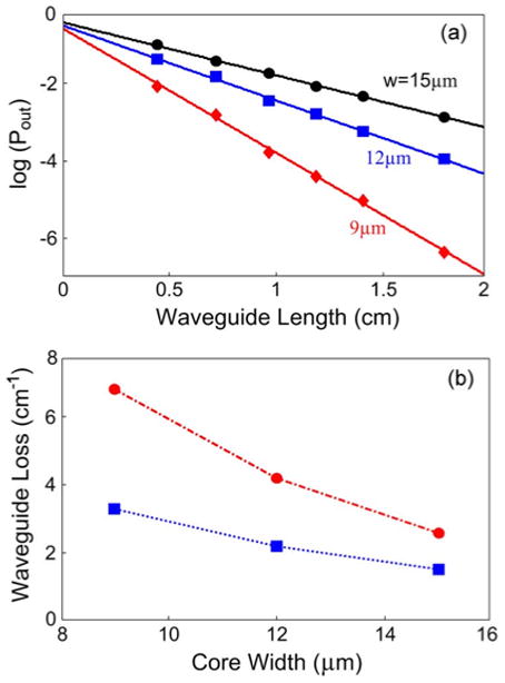
Previously, the lowest loss for air-core hollow ARROWs at 785 nm was achieved using the pre-etched pedestal design and was 2.6 cm−1 for a 5.8 × 15 μm hollow core [11]. To characterize the air-core loss for SAP ARROWs, the standard cutback method was used with light at 785 nm. Average losses were determined to be 3.31, 2.19, and 1.54 cm−1 for 9-, 12-, and 15-μm-wide waveguides, respectively. Losses for the two designs are shown in Fig. 4, and we see that losses for air-cores at 785 nm are greatly reduced for the SAP ARROWs for all three waveguide widths.
Fig. 4.

(a) Transmitted power versus SAP waveguide length with air-filled cores at 785 nm (symbols: experiment, lines: exponential fits). (b) Experimental hollow waveguide loss with air-filled cores at 785 nm for different core widths (height = 5.8 μm; circles: ARROWs on pre-etched substrates, squares: ARROWs on SAPs.
In conclusion, we have presented a new SAP design and fabrication method for hollow ARROW waveguides that produces nearly ideal hollow-core geometries. Air-core devices fabricated with this new process have record-low losses at 785 nm and over 90% fabrication yield. For our current integrated ARROW platforms with 4-mm-long hollow waveguides, light transmission should be improved by more than two times with the SAP ARROWs, which will increase sensitivity and performance of ARROW-based sensing and spectroscopy devices.
Acknowledgments
This work was supported by the NIH/NIBIB (Grant R01-EB006097), by the NSF (Grant ECS-0528714 and Grant ECS-0528730), and by the W. M. Keck Center for Nanoscale Optofluidics at UCSC.
Footnotes
Color versions of one or more of the figures in this letter are available online at http://ieeexplore.ieee.org.
Contributor Information
Evan J. Lunt, Email: van.lunt@gmail.com, Department of Electrical and Computer Engineering, Brigham Young University, Provo, UT 84602 USA.
Bin Wu, Email: binwu@soe.ucsc.edu, School of Engineering, University of California Santa Cruz, Santa Cruz, CA 95064 USA.
Jared M. Keeley, Email: jamakee@hotmail.com, Department of Electrical and Computer Engineering, Brigham Young University, Provo, UT 84602 USA
Philip Measor, Email: pmeasor@soe.ucsc.edu, School of Engineering, University of California Santa Cruz, Santa Cruz, CA 95064 USA.
Holger Schmidt, Email: hschmidt@soe.ucsc.edu, School of Engineering, University of California Santa Cruz, Santa Cruz, CA 95064 USA.
Aaron R. Hawkins, Email: hawkins@ee.byu.edu, Department of Electrical and Computer Engineering, Brigham Young University, Provo, UT 84602 USA.
References
- 1.Korampally V, Mukherjee S, Hossain M, Manor R, Yun M, Gangopadhyay K, Polo-Parada L, Gangopadhyay S. Development of a miniaturized liquid core waveguide system with nanoporous dielectric cladding—A potential biosensing platform. IEEE Sensors J. 2009 Dec;9(12):1711–1718. [Google Scholar]
- 2.Datta A, Eom IY, Dhar A, Kuban P, Manor R, Ahmad I, Gangopadhyay S, Dallas T, Holtz M, Temkin H, Dasgupta P. Micro-fabrication and characterization of Teflon AF-coated liquid core waveguide channels in silicon. IEEE Sensors J. 2003 Dec;3(6):788–795. [Google Scholar]
- 3.Abouraddy AF, Bayindir M, Benoit G, Hart SD, Kuriki K, Orf N, Shapira O, Sorin F, Temelkuran B, Fink Y. Towards multimaterial multifunctional fibres that see, hear, sense and communicate. Nat Mater. 2007 May;6(5):336–347. doi: 10.1038/nmat1889. [DOI] [PubMed] [Google Scholar]
- 4.Ponnampalam N, DeCorby RG. Self-assembled hollow waveguides with hybrid metal-dielectric Bragg claddings. Opt Express. 2007;15(20):12595–12604. doi: 10.1364/oe.15.012595. [DOI] [PubMed] [Google Scholar]
- 5.Yin D, Schmidt H, Barber J, Hawkins A. Integrated ARROW waveguides with hollow cores. Opt Express. 2004;12(12):2710–2715. doi: 10.1364/opex.12.002710. [DOI] [PubMed] [Google Scholar]
- 6.Bernini R, De Nuccio E, Minardo A, Zeni L, Sarro P. 2-D MMI devices based on integrated hollow ARROW waveguides. IEEE J Sel Topics Quantum Electron. 2007 Mar./Apr;13(2):194–201. [Google Scholar]
- 7.Duguay MA, Kokubun Y, Koch TL, Pfeiffer L. Antiresonant reflecting optical waveguides in SiO2 – Si multilayer structures. Appl Phys Let. 1986;49(1):13–15. [Google Scholar]
- 8.Kühn S, Measor P, Lunt EJ, Phillips BS, Deamer DW, Hawkins AR, Schmidt H. Loss-based optical trap for on-chip particle analysis. Lab Chip. 2009;9(15):2212–2216. doi: 10.1039/b900555b. [DOI] [PMC free article] [PubMed] [Google Scholar]
- 9.Rudenko M, Kuhn S, Lunt E, Deamer D, Hawkins A, Schmidt H. Ultrasensitive Qβ phage analysis using fluorescence correlation spectroscopy on an optofluidic chip. Biosens Bioelectron. 2009;24(11):3258–3263. doi: 10.1016/j.bios.2009.04.005. [DOI] [PMC free article] [PubMed] [Google Scholar]
- 10.Wu B, Hulbert J, Hawkins A, Schmidt H. Planar hollow-core waveguide technology for atomic spectroscopy and quantum interference in alkali vapors. J Lightw Technol. 2008 Dec 1;26(23):3727–3733. [Google Scholar]
- 11.Yin D, Barber J, Hawkins A, Schmidt H. Waveguide loss optimization in hollow-core ARROW waveguides. Opt Express. 2005;13(23):9331–9336. doi: 10.1364/opex.13.009331. [DOI] [PubMed] [Google Scholar]
- 12.Myneni S, Hess DW. Post-plasma-etch residue removal using CO2-based fluids. J Electrochem Soc. 2003;150(12):G744–G750. [Google Scholar]
- 13.Timmons CL, Hess DW. Photoresist and fluorocarbon post-plasma etch residue removal using electrochemically generated radical anions. J Electrochem Soc. 2008;155(10):H771–H777. [Google Scholar]
- 14.Lunt EJ, Phillips BS, Keeley JM, Hawkins AR, Measor P, Wu B, Schmidt H. Hollow ARROW waveguides on self-aligned pedestals for high-sensitivity optical sensing. Proc SPIE. 2010;7591:759109. [Google Scholar]


