Abstract
We demonstrate the optimization of the concentration, temperature and cycling of a piranha (H2O2:H2SO4) mixture that produces high yields while quickly etching hollow structures made using a highly crosslinked SU8 polymer sacrificial core. The effects of the piranha mixture on the thickness, refractive index and roughness of common micro-electromechanical systems and micro-opto-electromechanical systems fabrication materials (SiN, SiO2 and Si) were determined. The effectiveness of the optimal piranha mixture was demonstrated in the construction of hollow anti-resonant reflecting optical waveguides.
1. Introduction
Micro-electromechanical systems (MEMS) and micro-opto-electromechanical systems (MOEMS) technology include a large variety of applications that usually require 3D patterning of high aspect ratio structures. SU8 (MicroChem Corp.) is a negative tone, high resolution, chemically amplified, near-UV photoresist polymer that is used in many MEMS and MOEMS devices, both as a temporary, photolithographic and a permanent structural [1] material as shown in figure 1.
Figure 1.
SU8 coating applications flow diagram.
For example, SU8 is used as a temporary material for sacrificial etching of hollow waveguides [2], a photolithographic material for etch masks, plating, deposition [3], release layers [4] and wafer bonding layers [5], and a permanent material in soft lithography for building microfluidic devices [6], inkjet nozzles [7] and atomic force microscope (AFM) probe tips [8]. SU8 is also used for electroplating molds [3] and packaging coatings [9]. In addition, it has been investigated for many other applications, including as a low-cost material for the fabrication of large micro-mirror arrays [10]. The unique properties of SU8 make it an attractive material for fabrication of these types of structures [11]. SU8 is photosensitive between 300 and 400 nm and its transparency allows high aspect ratio patterning with smooth (9 nm rms), near-vertical sidewalls. Additionally, after development, it has a high thermal (250 °C) and chemical stability due to the highly crosslinked epoxy rings of the SU8 molecules. This means that SU8 structures can be easily patterned using photolithography and maintain their geometries at the high temperatures at which CVD layers are typically deposited. However, some of the properties that make SU8 an attractive sacrificial material from a structural standpoint also make it difficult to sacrificially remove. For this reason, SU8 is often avoided as a sacrificial material.
Highly crosslinked, UV-exposed SU8 can be removed from the surface of substrates by dissolution using solvents such as N-methylpyrrolidone (NMP), liftoff processes accomplished by depositing SU8 on omnicoat layers, and acids such as hydrochloric acid, sulfuric acid, nanostrip ((H2SO4:H2SO5:H2O2:H2O) (9:0.5:0.1:0.5)) (Cyantek Corp.), and Aqua Regia ((HNO3:HCl) (1:3)). These methods work well for the removal of small amounts of SU8 when fabricating features such as voids or gaps [12, 13] as shown in figure 2(a). However, these techniques are difficult to use (or produce very low etch rates) when removing large amounts of SU8, as can be the case when fabricating release layers [14] and long microfluidic channels (~1 cm) with complicated 3D geometries processed at high temperatures [2] as shown in figures 2(b) and (c).
Figure 2.
The different uses of SU8 for fabrication of (a) voids and gaps, (b) release layers and (c) long hollow channels.
In this work, the use of an optimized piranha (H2O2:H2SO4) mixture, that is used to remove SU8 that has been highly crosslinked and heated to high temperatures (~250 °C), is examined. Piranha mixtures have been used in the past to remove SU8; however these mixtures suffer from low etch rates and device yields due to vigorous chemical etching processes [15]. In order to overcome these challenges, different concentrations and temperatures of piranha mixtures were tested to find an optimal mixture that maximizes the etch rate of SU8 and the device yield of sacrificially etched MEMS structures shown in figure 2. Microfluidic channels are probably the most challenging structures to construct of those shown in figure 2, therefore we have chosen to specifically investigate them in this work. The conclusions drawn for microfluidic channels, should apply directly to the other structures. Because microfluidic channels can also be used for optical applications, we determined the effects on the roughness, thickness and index of refraction of exposure to piranha mixtures for SiN, SiO2 and Si solid-state thin films. Finally an anti-resonant reflecting optical waveguide (ARROW) was demonstrated using SU8 as a sacrificial core material and an optimized piranha mixture to remove the SU8. The ARROW is an extreme example of an opto-microfluidic channel which must have precise, uniform film layers for optical sensing and features lengths of (~4 mm) and a large length/cross-section ratio of 165/1 [2].
2. SU8 and piranha
The SU8 polymer was originally developed and patented by IBM-Watson Research Center (Yorktown Height-USA, US Patent No. 4882245 (1989) and others). In 1996, the material was adapted for MEMS applications [16]. SU8 consists of three basic components: an epoxy called Epon SU8, a solvent called gamma-Butyrolactone (GBL) and a photoacid generator taken from the family of the triaryliumsulfonium salts. During exposure to UV light, the photoacid is photochemically produced in the solid photoresist film upon absorption of light. The photoacid acts as a catalyst in the subsequent cross-linking reaction that takes place during post-exposure baking (PEB). The cross-linking reaction takes place in a ‘zipping up’ fashion, where each epoxy group can react with another epoxy group in different SU8 molecules.
The piranha mixture has a long history of use in the semiconductor industry for cleaning silicon wafers by removing organic residues [17]. The effectiveness of the piranha mixture in removing the SU8 polymer is due to two processes, dehydration and oxidation. The first process, dehydration of the SU8 or hydration of sulfuric acid, involves the removal of hydrogen and oxygen from the SU8 molecules by concentrated sulfuric acid. The second process, oxidation, is the sulfuric acid’s increased conversion of hydrogen peroxide from a relatively mild oxidizing agent into one sufficiently aggressive to dissolve elemental carbon. Each of these chemical processes allows the chemical bonds of the individual and linked SU8 molecules to be broken. In time, SU8 which is immersed in piranha mixtures will typically be completely removed, with no visible traces of the original organic materials remaining.
3. Characterization of piranha etch rates of SU8
In order to characterize the etch rate of SU8 immersed in piranha mixtures with different concentrations and temperatures, long (~4 mm) microfluidic channels were fabricated using SU8 as the sacrificial core material. Microfluidic channels were made by depositing and patterning straight lines of a SU8-10 polymer with dimensions of width 12 µm, height 5 µm and length 1 cm on 4 inch silicon wafers as shown in figure 3(a) [18].
Figure 3.
Fabrication flow diagram of SiO2 microfluidic channels. (a) Deposition and patterning of the SU8 polymer. (b) PECVD SiO2 overcoat layer. (c) SU8 sacrificial core removed.
The process of depositing the SU8 began by cleaning the silicon wafer with an O2 descum (Technic Planar Etch II) at a gas flow rate of 10 sccm O2, at a pressure of 350 mTorr and a power of 100 W for 60 s. A 6 mL quantity of SU8 was then poured on the silicon wafer and spun (Laurell Spin Processor) at 500 rpm for 6 s, 4400 rpm for 60 s and 6000 rpm for 2 s. The SU8 was then soft baked on a hotplate at 95 °C for 10 min and then allowed to cool for 5 min at room temperature. Next, the wafer was patterned by aligning (Karl Suss MA 150 CC) and exposing it to a dose of 140 mJ cm−2 broadband collimated UV light using a 350 W mercury bulb. A postexposure bake (PEB) was then performed for 10 min at 95 °C and then the wafer was allowed to cool for 5 min at room temperature. The SU8 was then developed by immersing the wafer in the SU8 developer and agitating it for 1.5 min, removing and rinsing it with IPA and blowing it dry with nitrogen. Finally, the SU8 was hard baked on a hotplate at 260 °C for 30 min to further crosslink the polymer and to make it more thermally resistant. The resulting SU8 structure has smooth, vertical sidewalls and a thickness of 5 µm. The SU8 was covered with a 3 µm layer of PECVD SiO2 grown with a mixture of 5% silane in helium (SiH4/He) and nitrous oxide (N2O), at 250 °C and 600 mTorr deposition pressure as shown in figure 3(b). The SU8 was exposed by cleaving an end of the microfluidic channels. The microfluidic channels were then submerged in the piranha mixtures using custom teflon wafer chip holders and the SU8 was removed as shown in figure 3(c). The etch rate of the SU8 in the piranha mixture was determined by measuring the amount of SU8 remaining in the microfluidic channel after a given time using a light microscope (Leica DM LB 100T) with a 20× magnification objective.
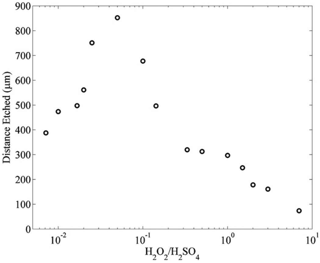
In order to determine how the concentration of the piranha mixture effects the etch rate of the sacrificial SU8, the microfluidic channels were immersed in several different concentrations of piranha mixtures for 1 h while the mixture was held at a constant temperature of 100 °C. Figure 4 shows that the piranha mixture with a ratio of (1:20) (H2O2:H2SO4) produces the highest etch rate of SU8.
Figure 4.
The distances etched for microfluidic channels with SU8 sacrificial cores immersed in different concentrations of piranha mixtures for 1 h at 100 °C.
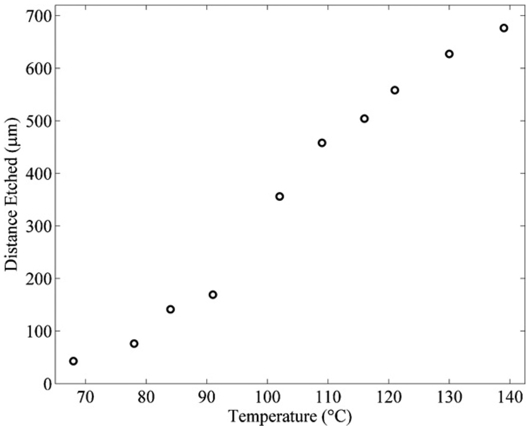
The temperature of the piranha mixture also plays an important role in the speed of the etch rate of SU8 [19]. In order to examine these effects, we immersed our microfluidic channels in piranha (1:1) (H2O2:H2SO4) mixtures for 1 h at temperatures of 65 –140 °C. Figure 5 shows that as the temperature is increased, the etch rate of the SU8 increases monotonically.
Figure 5.
The distances etched for microfluidic channels with SU8 sacrificial cores immersed in a piranha mixture with a ratio of (1:1) (H2O2:H2SO4) at temperatures ranging from 65 to 140 °C for 1 h.
4. Optimization of piranha mixture for 100% yield
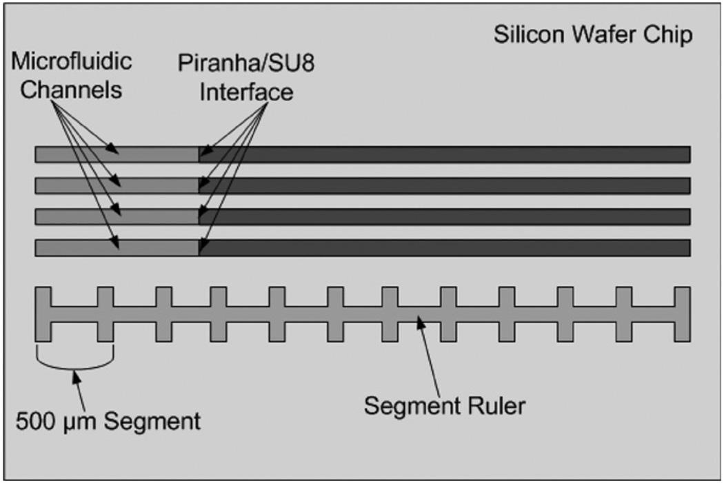
While it is desirable to use a piranha mixture that produces the highest etch rate for SU8, it is also important that the piranha mixture produce high yields for MEMS and MOEMS devices. The piranha mixtures with higher ratios of sulfuric acid were expected to produce lower yields because the sulfuric acid is much more viscous (26.7 cP at 20 °C) than hydrogen peroxide (1.245 cP at 20 °C) [20]. The increased viscosity of higher concentration sulfuric acid causes gases produced during the reaction of piranha with the SU8 polymer, such as CO2, O2 and H2O, to diffuse much more slowly over long distances. The slower diffusion rates cause higher pressures to build up within longer hollow structures leading to more breaks and cracks [15]. In order to determine the optimal piranha mixture for maximizing yield, the microfluidic channels described in section 3 were immersed in several different piranha mixtures with different concentrations and temperatures. The fabrication yield of the microfluidic channels was calculated by considering the microfluidic channels to be separated into 500 µm segments determined by the segment ruler. The microfluidic channels were examined to determine if any breaks or cracks occurred within a segment as shown in figure 6.
Figure 6.
The top view of the microfluidic channel setup for determining the fabrication yield percentage of different concentrations and temperatures of piranha mixtures.
If a segment of the microfluidic channel had a break or crack within the entire length of the segment, the entire segment was considered to have failed. The percentage of fabrication yield of the microfluidic channel was then calculated by dividing the number of completely intact segments by the total number of segments in a microfluidic channel using
| (1) |
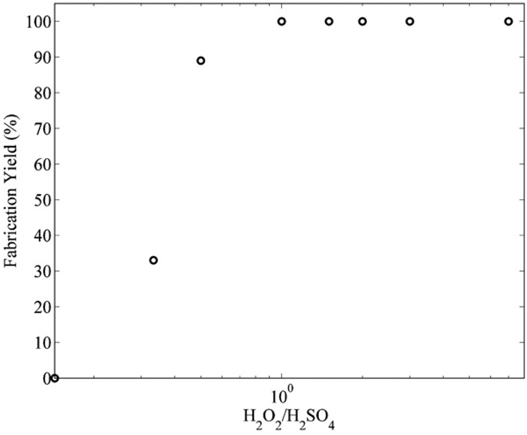
Figure 7 shows that a piranha mixture with a ratio of (1:1) (H2O2:H2SO4) at 100 °C contained the maximum concentration of H2SO4 that could be added to the piranha mixture before the microfluidic channels fabrication yield decreased below 100%.
Figure 7.
The fabrication yields for microfluidic channels with SU8 sacrificial cores immersed in different piranha mixture concentrations for 24 h at 100 °C.
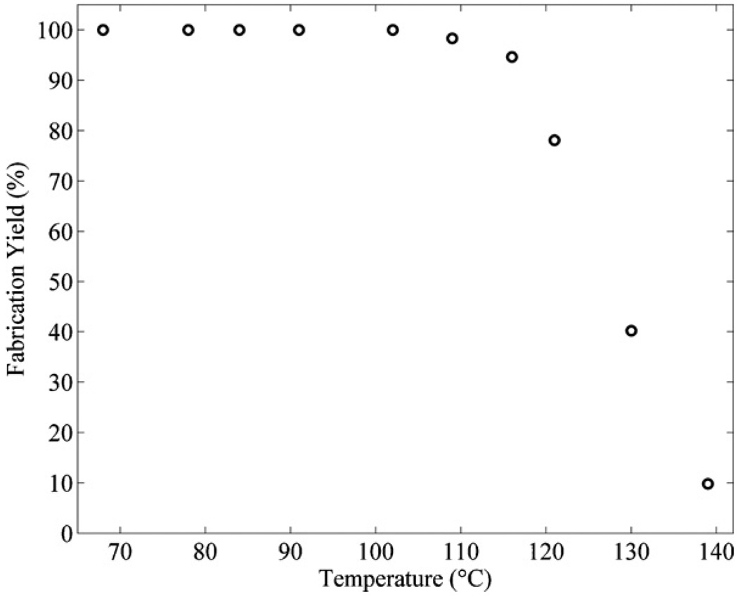
Figure 8 shows the fabrication yield for microfluidic channels immersed in piranha mixtures with a ratio of (1:1) (H2O2:H2SO4) for 1 h at temperatures between 65 and 140 °C. Microfluidic channels immersed in piranha mixtures above 100 °C tend to cause breaking and cracking due to more vigorous chemical reactions and increased gas pressures. Therefore, we have determined that the optimal etch temperature for the piranha mixture with a ratio of (1:1) (H2O2:H2SO4) that produced 100% fabrication yields was 100 °C for the particular microchannel geometry and overcoating described in section 3.
Figure 8.
The fabrication yields for microfluidic channels with SU8 sacrificial cores immersed in different piranha mixtures with a ratio of (1:1) (H2O2:H2SO4) for 1 h at temperatures from 65 to 140 °C.
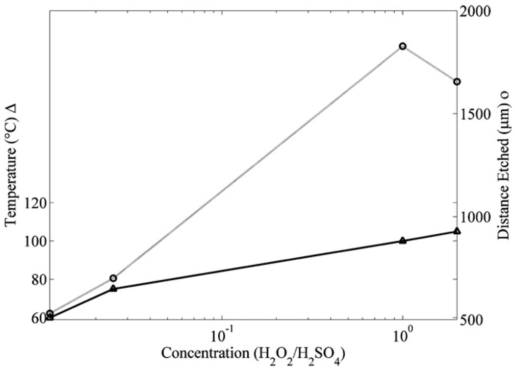
Finally, in order to determine the optimal piranha mixture concentration and temperature for the fastest SU8 etch rate with a 100% microfluidic channel yield, we repeated the optimization testing for several different piranha mixtures. For example, microfluidic channels made with SU8 sacrificial cores were immersed in the piranha mixture with a ratio of (1:40) (H2O2:H2SO4) at temperatures varying between (60 and 120 °C) for 1 h. From these experiments, it was determined that the highest temperature piranha mixture the channels could be immersed in with a 100% fabrication yields was 78 °C. The etch distance of the SU8 was then measured to be 700 µm. This process was repeated for several different concentrations of piranha mixtures. Figure 9 shows that the piranha mixture with a ratio of (1:1) (H2O2:H2SO4) has the highest SU8 etch rate for the maximum temperature that produces 100% fabrication yields for the particular microfluidic channel geometry and overcoating described in section 3.
Figure 9.
The maximum temperatures for piranha mixtures at different concentrations that still produces 100% fabrication yields (circles and light gray line) after 1 h of etching. Also shown are the distances etched in the microfluidic channels for the different concentrations and temperatures after 1 h (triangles and black line).
The results in figure 9 are for one specific channel geometry; however, when different channel geometries are used, key processing conditions can be modified to provide the highest SU8 etch rates while maintaining a 100% fabrication yield. For each different microfluidic channel geometry, there is a maximum internal pressure that the microfluidic channel can withstand before it is damaged, which is defined as the critical pressure. The key processing conditions which affect the critical pressure are the geometry of the microfluidic channel and the concentration and temperature of the piranha mixture. In order to produce 100% fabrication yields, the parameters of the key processing conditions must be determined so that the critical pressure of the microfluidic channel geometry is not exceeded. Some general guidelines describing how these parameters should be adjusted can be determined from previous experiments [15, 21, 22].
First, if the width of a rectangular channel made with SU8 is increased, it is important to increase the thickness of the channel overcoat layer so that for a given concentration and temperature of piranha mixture, the critical channel pressure is not exceeded. The critical pressure scales with channel geometry as
| (2) |
where Pc is the critical channel pressure, th is the thickness of the overcoat material and w is the width of the channel. For example, when using a piranha mixture with a ratio of (1:1) (H2O2:H2SO4) and a temperature of 100 °C, the ratio th/w ≥ 1/4 keeps the channel pressure below the critical channel pressure. This produces 100% fabrication yields of the microfluidic channels that were described in section 3.
Second, from equation (2), if th/w ≫ 1/4, then the microfluidic channels can withstand higher internal pressures. It is expected that the increased temperature of the piranha mixture would produce increased SU8 etch rates that would follow a similar trend as the SU8 etch rates in figure 9.
5. Self-decomposition of H2O2 and diffusion-limited etching
There are two other effects that need to be considered when determining how quickly piranha mixtures etch SU8. The first effect is diffusion-limited etching in long microfluidic channels and the second effect is the reduced concentrations of H2O2 in the piranha mixture, due to self-decomposition of H2O2 into H2O and O2. Both of these effects cause the etch rate of the SU8 to be reduced over time. First, for a sufficiently long etch distances, the etch rate of long microfluidic channels is diffusion limited and the etch length follows the diffusion equation,
| (3) |
where l(t) is the length of the microfluidic channel etched, ρ is the density of the SU8 in solid form, Cs is the saturation concentration of the SU8 in the piranha mixture at the interface surface, Cb is the concentration of SU8 in the bulk piranha mixture and D is the diffusion constant for the SU8 through the piranha mixture in the microfluidic channel [21–26,] as shown in figure 10.
Figure 10.
Model for the diffusion process that piranha uses to etch SU8 from the microfluidic channels.
Second, the reduced etch rate of the SU8 due to self-decomposition of H2O2 can also be determined by the diffusion equation. However, the parameters that describe the concentration of SU8 in the piranha mixture, Cs and Cb, are reduced because of the reduced concentration of H2O2 in the piranha mixture.
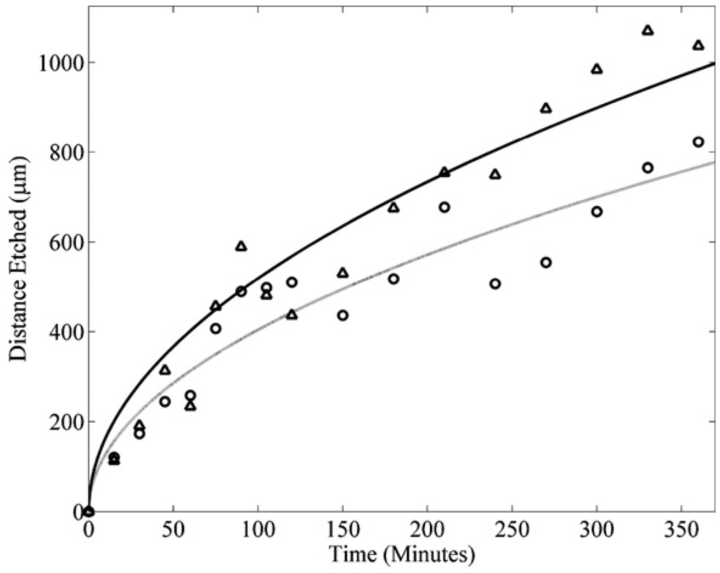
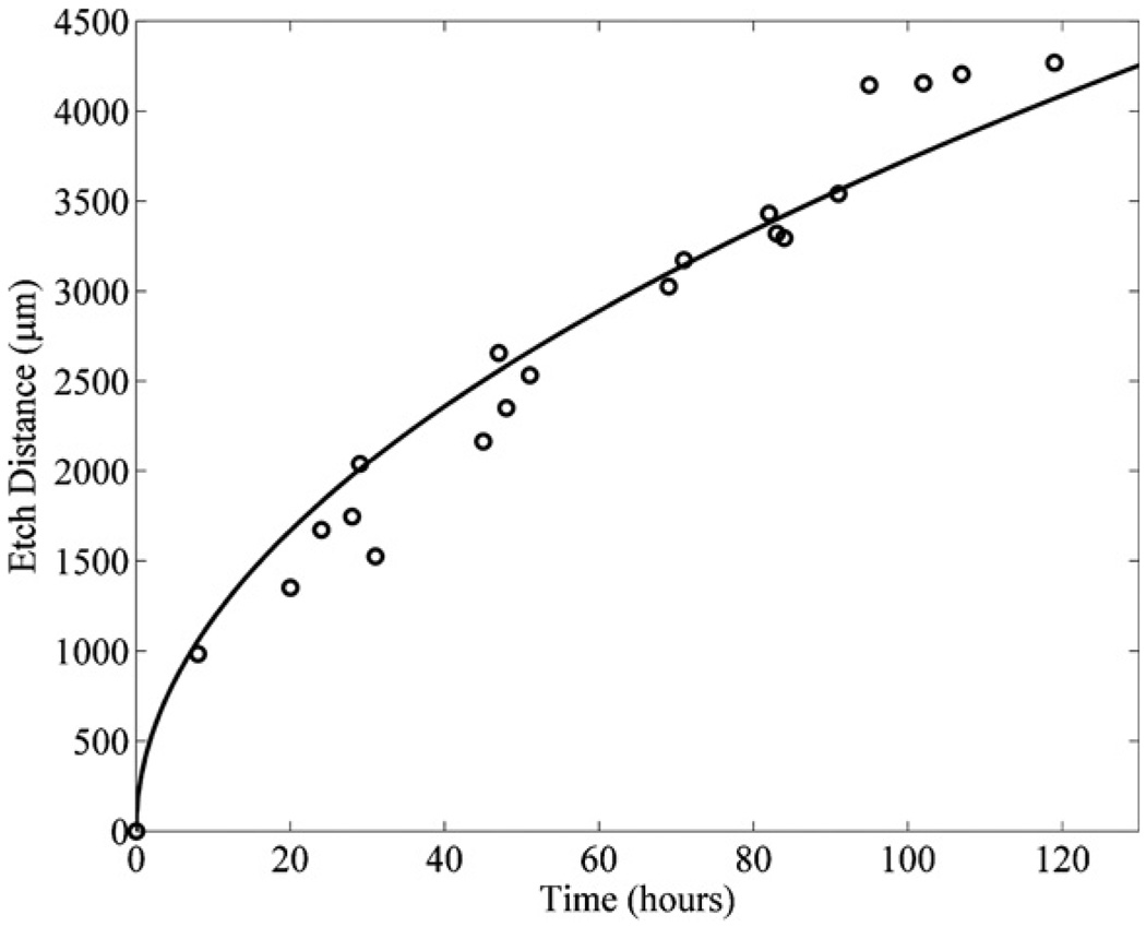
The timeframe, for which the decomposition of hydrogen peroxide significantly decreases the etch rate of the SU8 by the piranha mixture, can be determined experimentally. This was done by immersing the microfluidic channels described in section 3 in a piranha mixture with a ratio of (1:1) (H2O2:H2SO4) that was changed every hour, and in a similar mixture that was not changed over a 6 h period. The measured distances of the SU8 etched by the piranha mixture changed every hour (triangles) and the piranha mixture that was not changed (circles) are shown in figure 11. Curves with square root dependence (corresponding to equation (3)) were fit to the data sets in figure 11. The equations matched to these curves are given by the following: l(t) = (52t)1/2 for the piranha mixture changed every hour (solid line) and l(t) = (40t)1/2 for the piranha mixture that was not changed (light gray dotted line) over the 6 h period. The data show that a deviation of 10% in the etch rates of the SU8 occurs between 60 and 90 min. It was determined that the piranha mixture should be replenished with hydrogen peroxide at least every 60–90 min to maintain consistently high etch rates of the SU8 in the microfluidic channels. When the piranha mixture is changed every 60–90 min the fitted diffusion curve predicts that a 4 mm microfluidic channel will finish etching in 100 h. However, this can be expensive and time consuming. In practice, the piranha mixture was changed in 24 h intervals which were shown experimentally to etch 4 mm microfluidic channels in 120 h as shown in figure 12. The loss of 20 h of processing time, in this case, was acceptable in order to reduce the cost of continually replenishing the high concentration H2O2 in the piranha mixture.
Figure 11.
The distances etched for microfluidic channels with SU8 sacrificial cores immersed in piranha mixtures with a ratio of (1:1) (H2O2:H2SO4) at 100 °C for 6 h that were replaced every hour (triangles and solid line) and the microfluidic channels for which the mixture was not replaced (circles and light gray dotted line) reflecting a decreased distance etched due to the effects of H2O2 self decomposition.
Figure 12.
The distances etched for a 4 mm long microfluidic channel with SU8 sacrificial cores in a piranha mixture with a ratio of (1:1) (H2O2:H2SO4) at 100 °C for 120 h with a replacement frequency of 24 h (circles and black line).
6. Microfluidic channels/waveguide optical properties
Waveguides and other optical elements are increasingly being used in conjunction with microfluidic channels to deliver light to microfluidic channels for optofluidic applications [27–29]. Waveguides, microfluidic channels and supporting MEMS and MOEMS devices can be made out of many different materials. However, SiN, SiO2 and Si are commonly used because they are prominent in silicon manufacturing. When using these materials, it is important that their optical properties are unchanged after they are immersed in piranha mixtures. Specifically, it is important that the piranha mixtures do not significantly etch, roughen or change the index of the SiN, SiO2 or Si.
6.1. Fabrication of films and structures to measure the optical properties of SiN, SiO2 and Si
In order to determine if the piranha mixture etches, roughens or changes the index of SiN and SiO2, films were grown at 250 °C on 4 inch silicon wafers and placed in a piranha mixture with a ratio of (1:1) (H2O2:H2SO4) at 100 °C for 24 h. The SiN was grown with a PECVD system with a mixture of 5% silane in helium (SiH4/He) and ammonia (NH3), at 250 °C, and 1 Torr deposition pressure. The SiO2 was also grown with a PECVD system with a mixture of 5% silane in helium (SiH4/He) and nitrous oxide (N2O), at 250 °C and 600 mTorr. In order to determine the effects of the piranha mixture on Si, a blank 4 inch silicon wafer was also placed in a piranha mixture with a ratio of (1:1) (H2O2:H2SO4) at 100 °C for 24 h.
6.2. Effect of piranha on the roughness of SiN, SiO2, and Si films
Table 1 shows the atomic force microscopy (Digital Instrument Dimension 3100) (AFM)-measured root mean square (rms) roughness (with a test accuracy within 0.2–0.3 nm) of our SiN, SiO2 and Si before and after they were immersed in piranha. It was determined from the AFM measurements that the roughness of the films was not significantly affected by immersion in the piranha mixture and therefore additional loss due to the scattering mechanisms is not expected. Note that the roughness measurements shown in table 1 are for films deposited directly on Si substrates or the substrates themselves. When films are deposited over SU8 sacrificial cores, the roughness of the SU8 will translate into the SiN and SiO2 films. AFM measurements of the top of patterned and processed SU8 lines have shown a roughness of 30–40 nm rms.
Table 1.
The AFM rms roughness measurements for PECVD SiN and SiO2 deposited at 250 °C and Si before and after they are immersed in piranha mixture with a ratio of (1:1) (H2O2:H2SO4) at 100 °C for 24 h.
| Film | Roughness of film (nm) |
Roughness of piranha (1:1) etched film (nm) |
|---|---|---|
| Si | 0.3853 (±0.09) | 0.3265 (±0.04) |
| SiN | 1.295 (±0.12) | 0.9527 (±0.04) |
| SiO2 | 1.8420 (±0.15) | 1.4133 (±0.04) |
6.3. Effect of piranha on the thickness and index of refraction of SiN, SiO2 and Si
It is also important that the refractive indices and thicknesses of the SiN, SiO2 and Si are not significantly altered by immersion in the piranha mixture. Previous work has found that the etch rate of PECVD SiO2 and Si are 0 nm min−1, and the etch rate for SiN is 0.016 nm min−1 in a piranha mixture that is (98% H2SO4:30% H2O2) with a concentration of (50:1) at 120 °C [30]. We performed similar tests using a piranha mixture with a ratio of (1:1) (H2O2:H2SO4) at 100 °C. Ellipsometry (Gaertner Scientific Corporation Model No. 1169-AK) and spectral reflectance (F20 Film Measurement System Model No.: 205–0135) systems were used to measure the refractive index and thickness of the SiN and SiO2 films. The refractive index of the SiO2 and SiN films did not have measurable differences within a test accuracy of 0.005. The SiN and SiO2 etch rates were determined by measuring the difference between the initial and final thicknesses of the SiN and SiO2 films. The etch rate of Si was determined using AFM measurements to detect a decrease in the film thickness when scanned over the surface of patterned Si structures. The SiO2 and Si did not have a measurable etch rate after immersion in the piranha mixture, however the etch rate of the SiN film was 0.14 nm h−1 and 0.17 nm h−1 when measured with spectral reflectance and ellipsometry, respectively. This has important consequences if a MEMS device constructed with SiN requires precise film thicknesses or is immersed in the piranha mixture for an extended amount of time.
7. ARROWs and piranha etching
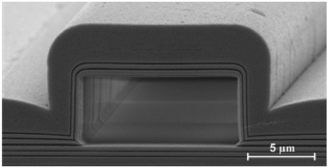
Microfluidic channels created using SU8 sacrificial etching have been used to form hollow anti-resonant reflecting optical waveguides [2, 25, 28, 29, 31, 32]. ARROWs are an excellent example of the application of SU8 sacrificial cores. They utilize the unique properties of SU8 to form a hollow microfluidic channel with a complicated geometry and vertical sidewalls surrounded by a dielectric layer stack that maximizes its waveguiding properties. ARROWs can be used to perform optical fluorescence sensing and detecting of single particles by guiding light through low index liquids and gasses inside their hollow cores [33–36]. Hollow ARROW microfluidic channels were fabricated by depositing alternating dielectric layers that act as Fabry–Perot reflectors. This allows light to be guided within the hollow core of the ARROW when the dielectric layers are grown at precise thicknesses fulfilling the antiresonant condition for maximum reflection into the waveguide core [2]. PECVD SiN and SiO2 were used as dielectric layers at thicknesses of toxide = 270 nm and tnitiride = 93 nm when nnitride =2.05, noxide =1.46, nc =1.33, dc =5 µm and λ = 633 nm, to form an ARROW with low propagation loss over a broad wavelength range from 500 to 700 nm. The optimized piranha mixture with a ratio of (1:1) (H2O2:H2SO4) at 100 °C was used to sacrificially etch SU8 cores producing ARROWs that were 4 mm long with 100% fabrication yields in 120 h. This represents a significant improvement over the well-established ARROW fabrication process that uses Nanostrip, a commercially available piranha mixture with a ratio of (9:0.5:0.1:0.5) (H2SO4:H2SO5:H2O2:H2O) (Cyantek Corp.), which typically produces 100% ARROW fabrication yields in 6–8 weeks. Figure 13 shows an SEM of the cross section of the finished ARROW device after the SU8 sacrificial core has been removed. The dark lines are the SiN layers, the lighter lines are the SiO2 layers and the central region is the removed SU8 sacrificial core area.
Figure 13.
An SEM image of the cross section of a hollow ARROW microfluidic channel after the complete removal of the SU8 polymer core in a piranha mixture with a ratio of (1:1) (H2O2:H2SO4) at 100 °C for 120 h.
8. Conclusions
In conclusion, we investigated the use of SU8 as a sacrificial material for the construction of MEMS and MOEMS devices. A process was determined to identify an optimal piranha mixture for the removal of SU8 sacrificial material from microfluidic channels. This was accomplished by varying the concentration and temperature of piranha mixtures to produce 100% fabrication yields and then observing which mixture produced the highest SU8 etch rate. The piranha mixture with a ratio of (1:1) (H2O2:H2SO4), a temperature of 100 °C and replenishment frequency of 24 h produced 100% fabrication yields and the highest SU8 etch rate for microfluidic channels with the geometry described in section 3. This mixture did not affect the thickness or index of SiO2 and Si. It also does not affect the index of SiN. However, it does etch SiN slowly. The roughness of the SiN, SiO2 and Si films were all unaffected upon immersion in the piranha mixture and, therefore, should not impact optical surface scattering loss. To demonstrate structures that can be made with SU8 sacrificial etching, long (~4 mm) ARROW microfluidic channels with stringent requirements on layer quality and complicated dielectric layer stacks were fabricated with sacrificial SU8 cores. However, piranha mixtures can be optimized for many different applications that use SU8 as a sacrificial material such as fabricating voids, gaps or release layers. In a high volume fabrication environment, the optimization of the piranha mixtures could significantly increase device fabrication yields and decrease fabrication production time leading to higher throughput and more cost-effective manufacturing processes.
Acknowledgments
We gratefully acknowledge financial support from the NIH/NIBIB (grant R01-EB006097), the NSF (grants ECS-0528714 and ECS-0528730) and the W. M. Keck Center for Nanoscale Optofluidics at UCSC.
Contributor Information
Matthew Holmes, Email: mattrholmes@ee.byu.edu.
Aaron Hawkins, Email: hawkins@ee.byu.edu.
References
- 1.Liu J, Cai B, Shu J, Ding G, Zhao X, Yang C, Chen D. Microsyst. Technol. 2004;10:265–268. [Google Scholar]
- 2.Yin D, Schmidt H, Barber JP, Hawkins AR. Opt. Exp. 2004;12:2710–2715. doi: 10.1364/opex.12.002710. [DOI] [PubMed] [Google Scholar]
- 3.Ghantasla M, Hayes J, Harvey E, Sood D. J. Micromech. Microeng. 2001;11:133–139. [Google Scholar]
- 4.Agirregabiria M, Blanco FJ, Berganzo J, Arroyo MT, Fullaondo A, Mayora K, Ruano-Lopez JM. Lab Chip. 2005;5:545–552. doi: 10.1039/b500519a. [DOI] [PubMed] [Google Scholar]
- 5.Svasek P, Svasek E, Lendl M, Vellekoop M. Sensors Actuators A. 2004;115:591–599. [Google Scholar]
- 6.Sato H, Matsumura H, Keino S, Shoji S. J. Micromech. Microeng. 2006;16:2318–2322. [Google Scholar]
- 7.Chung K, Lin C, Chen C, Fang Y, Tsai M. Microsyst. Technol. 2004;10:462–466. [Google Scholar]
- 8.Lee J, Shin H, Kim S, Hong S, Chung J, Park H, Moon J. Japan. J. Appl. Phys. 2003;42:L1171–L1174. [Google Scholar]
- 9.Zine-El-Abidine I, Okoniewski M. IEEE Trans. Adv. Packag. 2009;32:448–452. [Google Scholar]
- 10.Guerre R, Hibert C, Burri Y, Fluckiger P, Renaud P. Sensors Actuators A. 2005;123:570–583. [Google Scholar]
- 11.Conradie EH, Moore DF. J. Micromech. Microeng. 2002;12:368–374. [Google Scholar]
- 12.Chan K, Gleason K. J. Electrochem. Soc. 2006;153:C223–C228. [Google Scholar]
- 13.Daamen R, Bancken P, Nguyen V, Humbert A, Verheijden G, Hoofman R. Microelectron. Eng. 2007;84:2177–2183. [Google Scholar]
- 14.Pister K, Judy M, Burgett S, Fearing R. Sensors Actuators A. 1992;33:249–256. [Google Scholar]
- 15.Hubbard NB, Howell LL, Barber JP, Conkey DB, Hawkins AR, Schmidt H. J. Micromech. Microeng. 2005;15:720–727. [Google Scholar]
- 16.Lorenz H, Despont M, Fahrni N, Labianca N, Vettiger P, Renaud P. Proc. Micro Mechanics Europe’96 (Barcelona, IT, 1996) 1996:32–35. [Google Scholar]
- 17.Verhaverbeke S, Christenson K. Contamination-free Manufacturing for Semiconductor and Other Precision Products. New York: Dekker; 2001. [Google Scholar]
- 18.Yin D, Barber JP, Hawkins AR, Deamer DW, Schmidt H. Appl. Phys. Lett. 2004;85:3477–3479. [Google Scholar]
- 19.Ashe B, Giacofei C, Myhre G, Schmid AW. In: Laser-Induced Damage in Optical Materials. Exarhos GJ, Guenther AH, Lewis KL, Ristau D, Soileau MJ, Stolz CJ, editors. Bellingham, WA: SPIE; 2007. Proc. SPIE6720 67200N. [Google Scholar]
- 20.Lide D. CRC Handbook of Chemistry and Physics. 73rd edn. Boca Raton, FL: CRC Press; 1992. [Google Scholar]
- 21.Metz S, Jiguet S, Bertsch A, Renaud P. Lab Chip. 2004;4:114–120. doi: 10.1039/b310866j. [DOI] [PubMed] [Google Scholar]
- 22.Westberg D, Paul O, Andersson G, Baltes H. J. Micromech. Microeng. 1996;6:376–384. [Google Scholar]
- 23.Metz S, Bertsch A, Renaud P. J. Microelectromech. Syst. 2005;14:383–391. [Google Scholar]
- 24.Eaton W, Smith J, Jarecki R. Proc. SPIE. 1996;2879:80–93. [Google Scholar]
- 25.Lee J, Barber J, George Z, Lee M, Schmidt H, Hawkins A. J. Micro/Nanolith. MEMS MOEMS. 2007;6:013010–013017. [Google Scholar]
- 26.Howell L. Compliant Mechanisms. New York: Wiley; 2001. [Google Scholar]
- 27.Fleger M, Neyer A. Microelectron. Eng. 2005;83:1291–1293. [Google Scholar]
- 28.Schmidt H, Hawkins A. Microfluid. Nanofluid. 2008;4:3–16. doi: 10.1007/s10404-007-0199-7. [DOI] [PMC free article] [PubMed] [Google Scholar]
- 29.Hawkins A, Schmidt H. Microfluid. Nanofluid. 2008;4:17–32. doi: 10.1007/s10404-007-0194-z. [DOI] [PMC free article] [PubMed] [Google Scholar]
- 30.Williams KR, Gupta K, Wasilik M. J. Microelectromech. Syst. 2003;12:761–778. [Google Scholar]
- 31.Barber J, Lunt E, George Z, Yin D, Schmidt H, Hawkins A. IEEE Photonics Technol. Lett. 2006;18:28–30. [Google Scholar]
- 32.Yin D, Lunt E, Rudenko M, Deamer D, Hawkins A, Schmidt H. Lab Chip. 2007;7:1171–1175. doi: 10.1039/b708861b. [DOI] [PubMed] [Google Scholar]
- 33.Moener WE, Fromm DP. Rev. Sci. Instrum. 2003;74:3597–3619. [Google Scholar]
- 34.Yin D, Lunt EJ, Barman A, Hawkins AR, Schmidt H. Opt. Exp. 2007;15:7290–7295. doi: 10.1364/oe.15.007290. [DOI] [PubMed] [Google Scholar]
- 35.Yin D, Barber JP, Deamer DW, Hawkins AR, Schmidt H. Opt. Lett. 2006;31:2136–2138. doi: 10.1364/ol.31.002136. [DOI] [PubMed] [Google Scholar]
- 36.Rudenko M, Kühn S, Lunt E, Deamer D, Hawkins A, Schmidt H. Biosens. Bioelectron. 2009;24:3258–3263. doi: 10.1016/j.bios.2009.04.005. [DOI] [PMC free article] [PubMed] [Google Scholar]


