Abstract
Soft-polymer based microparticles are currently being applied in many biomedical applications, ranging from bioimaging and bioassays to drug delivery carriers. As one class of soft-polymers, hydrogels are materials, which can be used for delivering drug cargoes and can be fabricated in controlled sizes. Among the various hydrogel-forming polymers, poly(ethylene glycol) (PEG) based hydrogel systems are widely used due to their negligible toxicity and limited immunogenic recognition. Physical and chemical properties of particles (i.e., particle size, shape, surface charge, and hydrophobicity) are known to play an important role in cell-particle recognition and response. To understand the role of physicochemical properties of PEG-based hydrogel structures on cells, it is important to have geometrically precise and uniform hydrogel structures. To fabricate geometrically uniform structures, we have employed electron beam lithography (EBL) and ultra-violet optical lithography (UVL) using PEG or PEG diacrylate polymers. These hydrogel structures have been characterized by scanning electron microscopy (SEM), atomic force microscopy (AFM), optical microscopy, and attenuated total reflection Fourier-transform infrared spectroscopy (ATR-FTIR) confirming control of chemistry, size, and shape.
Indexing Chemicals: poly(ethylene glycol), poly(ethylene glycol) diacrylate, 2-hydroxy-4’-(2-hydroxyethoxy)-2-metylpropiophenone
I. INTRODUCTION
There is need for nano- and microparticles, or similar microstructures, in pharmaceutical applications including, but not limited to, imaging, bioassays, tissue engineering, and drug delivery carriers1–4. Utilizing conventional methodologies, nano- and microparticles are generally generated from lipids as micelles, liposomes, and solid lipid particles and from polymers as drug-encapsulated systems by precipitation5 and solvent evaporation, and drug conjugated systems by micelle formation6 and emulsion polymerization7–9. Several factors limit conventional methodologies, particularly polydispersity of particle size, limited control of shape, low drug loading efficiency, and poor control of drug release. Even though not completely understood, the physical and chemical properties of microparticles or microstructures (i.e., particle size, shape, surface charge and hydrophobicity, etc.) are known to play an important role in cell-particle recognition10–12. Therefore, the precise manipulation of physical and chemical properties of particles or structures is critical for biological applications.
To date, much research has been conducted generating controlled size and shape of nano-and microstructures via photolithographic methodologies13–14, nanoimprint lithography15, particle replication in non-wetting templates (PRINT)16, micro- and nanocontact printing methodologies17–18, and microfluidic devices19–20. Each method has benefits and limitations that are inherent in the method. Due to our experience with the techniques, two lithographic methodologies were used to fabricate nano- and microstructures of controlled sized and shape, enabling better understanding of the effects of these properties in biological applications. E-beam lithography allows very high resolution for small structures, but e-beam is limited by rate of production of structures. UV lithography allows much higher rate or microstructure production, but the resolution is more limited. In addition, these techniques allow fabrication of hydrogel structures.
Hydrogels are three-dimensional networks of polymer chains which swell in water and maintain their shape. Hydrogels have been investigated for many biological applications due to their biocompatibility, as well as their similarity of hydration and flexibility to nature tissue21–22. Poly(ethylene glycol) (PEG) is considered an excellent hydrogel material due to low toxicity and limited immunogenic recognition following implantation or injection23. PEG-based hydrogels have been synthesized using high-energy and low-energy radiation and the chemistries controlling the synthesis of PEG hydrogels are well known. Therefore, PEG-based hydrogel systems are useful for a myriad of biological applications such as drug delivery carriers in pharmaceutical applications, scaffolds in tissue engineering, as well as imaging, bioassays, and biosensors in biomedical applications.
In this paper, we report a method for preparing hydrogel structures using electron beam lithography26–27 (EBL) and ultra-violet optical lithography28 (UVL) as nano- and microfabrication techniques, respectively. Poly(ethylene glycol) (PEG) or PEG-diacrylate (PEGDA) hydrogel structures were created on silicon substrates by electron-beam or UV exposure, respectively. Fabricated hydrogel structures were then harvested by sonication, centrifuged, and finally dispersed in water for further analysis. With this approach, PEG-based hydrogel systems can be created simply by exposure to electron beam or UV light, thus providing an excellent platform for pharmaceutical applications.
II. EXPERIMENTAL DETAILS
A. Substrate preparation
A single-crystal silicon (Si) wafer of 10 cm diameter (<100>, Silicon Quest International) or a Si wafer section (1.5 cm × 1.5 cm) was used as a substrate for UVL or EBL, respectively. Si substrates were treated with a 4:1 (v/v) mixture of sulfuric acid (95%, ACS reagent grade, Acros organics) and hydrogen peroxide (30%, ACS reagent grade, Ricca Chemical Co.) for 10 minutes to clean the surfaces. Substrates were carefully rinsed with 17.5 MΩ cm resistivity de-ionized water. The substrate surface was dried with nitrogen gas and annealed on a hot plate at 200 °C for 5 minutes.
B. Polymer film preparation for electron beam lithography
A 10 (w/v) % poly(ethylene glycol) (PEG) (MW = 8,000 g/mole, Aldrich Chemical Co.) solution was prepared in N, N’-dimethylformamide (DMF) (Sequencing grade, Fisher Scientific). The polymer solution was filtered using a 0.25 μm filter. Filtered polymer solution (50 μL) was dispersed onto a Si section and spun at 4000 rpm for 60 seconds.
C. Polymer film preparation for ultra-violet optical lithography
A 30 (w/v) % poly(ethylene glycol) diacrylate (PEGDA) (MW = 3,400 g/mole, Laysan Biotech®) and 5 (w/v) % 2-hydroxy-4’-(2-hydroxyethoxy)-2-metylpropiophenone (Irgacure 2959®, Ciba) solutions were prepared in DMF separately as monomer and photoinitiator. After dissolving them in DMF, the solutions were filtered using a 0.25 μm filter individually. Immediately after combining 990 μL of PEGDA and 10 μL of Irgacure 2959, the solution (1 mL) was dispersed onto a Si wafer and spun at 1000 rpm for 90 seconds.
D. Hydrogel nanostructure fabrication
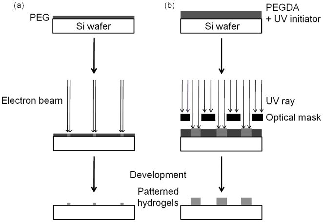
Hydrogel nanostructures were designed as disc and cubic shapes with lengths or diameters of 500 nm, 200 nm, and 50 nm, and a height of 160 nm. For electron beam exposure of hydrogel nanostructures we used a Raith 150 EBL system (Raith USA, Inc., Islip, NY) at 20 keV electron beam voltage and 0.34 nA current (figure 1 (a)). To study the effect of the electron beam dose and scattering with respect to resulting nanostructure size, a series of hydrogel nanostructure arrays were created by varying the beam dose and interstructure spacing. For a given electron beam current, the beam dose was varied to determine the effect on structure size, ranging from a starting dose of 250 μC/cm2 with increases of 25 μC/cm2 each step thereafter. We also varied the interstructure spacing (2μm, 3 μm, and 5 μm) to examine the proximity effect due to electron scattering. Immediately after exposure, the samples were developed in de-ionized water (17.5 MΩ cm resistivity) and dried in air.
Figure 1.
Schematic illustration of hydrogel structure fabrication by a) electron beam lithography and b) ultra-violet optical lithography.
E. Hydrogel microstructure fabrication
Hydrogel microstructures were designed as disc shapes with diameter of 1 μm to 2.5 μm in 0.5 μm increments, and a height of 1 μm. Hydrogel microstructures were fabricated by photocrosslinking while exposing a polymer film through an optical mask with ultraviolet (UV) light using a Karl Suss MA6 mask aligner (λ = 360 – 410 nm; dose range from 375 mJ/cm2 to 1125 mJ/cm2) in a vacuum contact mode (figure 1 (b)). The exposed sample was immediately developed in ethanol to remove unreacted polymer and crosslinking agent, with the fabricated hydrogel microstructures remaining on the Si wafer.
F. Characterization
Ellipsometry (λ=200 – 1200 nm; θ=70°, UVISEL Spectroscopic Phase Modulated Ellipsometer, HORIBA Jobin Yvon Inc, Edison, NJ) and stylus profilometery (Dektak® 8 Advanced Development Profiler, Veeco Ins., Plainview, NY) were used to determine the polymer film thickness on Si substrates. Data from ellipsometry were collected in air at room temperature and 40 % relative humidity. The thickness was determined by using the Cauchy absorbent model with an index of refraction n = 1.46 and the extinction coefficient κ = 029–30. The obtained values from ellipsometry were compared with the data from stylus profilometry. Fabricated hydrogel nanostructures were characterized by atomic force microscopy (AFM) (XE-HDD, PSIA Corp., South Korea) in non-contact mode and by scanning electron microscopy (SEM) using the Raith 150 with LEO SEM software. Fabricated hydrogel microstructures were characterized using an Olympus MX61 microscope in bright field mode. Attenuated total reflectance-Fourier transform infrared (ATR-FTIR) spectroscopy (Vertex 70 FT-IR spectrometer equipped with HYPERION™ series microscope, Bruker Optik GmbH, Ettlingen, Germany) was performed to analyze chemical modification induced by electron beam and UV light exposure.
G. Hydrogel structure release
PEGDA hydrogel microstructures were released in ethanol from Si wafers by sonication. The Si wafer was observed to confirm microstructure release after sonication using optical microscopy. The solution containing released hydrogel microstructures as freely suspended microparticles was transferred to a glass centrifuge tube (50 mL) for centrifugation (1800 g, 30 min) (GS-6R Centrifuge, Beckman Coulter). After resuspending the microparticles in fresh ethanol for two hours, the microparticles were centrifuged three more times. A final wash in fresh ethanol was continued overnight before recovery again by centrifugation. Following this final wash, hydrogel microparticles were air-dried to remove the ethanol and stored at −20 °C.
III. RESULTS AND DISCUSSION
A. Thickness measurements
A PEG film on Si section produced by spinning at 4000 rpm for 60 seconds had a thickness of 160 nm as determined from analysis of ellipsometer data. The measured thickness from ellipsometric data correlated well with the resulting stylus profilometer data of 158.3 nm. Similarly, a PEGDA film on Si wafer produced by spin coating at 1000 rpm for 90 seconds was determined to have a thickness of approximately 1 μm.
B. Effect of dose rate on hydrogel nanostructures
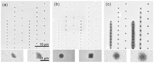
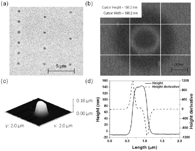
For EBL, hydrogel nanostructures were designed as disc and cubic shapes with lengths or diameters of 500 nm, 200 nm, and 50 nm for testing the resolution limit and the dose required to fabricate such features of different lengths or diameters. The effect of the electron beam dose was studied with respect to nanostructure size at a current of 0.34 nA. The full range of exposure doses for 500 nm hydrogel structures was from 250 μC/cm2 to 2725 μC/cm2 in 25 μC/cm2 dose steps. The final size of any given hydrogel structure was dose dependent for all of the shapes patterned. In particular, for the 500 nm hydrogel structures, hydrogel structures exposed at a dose lower than 600 μC/cm2 were irregularly shaped (figure 2(a)) due to underexposure and therefore incomplete crosslinking. Experimental results for doses between 600 to 1350 μC/cm2 indicate that hydrogel structure width is generally larger than expected and the width decreasing proportionally with an increase in beam dose at the low end of the dose range (Table 1). This result may be attributed to the fact that hydrogels exposed to higher dose have less swelling when they are immersed in water due to increased crosslinking with increased dose. Above 900 μC/cm2, the hydrogel structure width increased proportionally with an increase in beam dose (Table 1). It should be noted that increasing beam dose can cause an increase in structure width due to electron scattering (figure 2(b)). Especially for a dose above 1350 μC/cm2, at an interstructure spacing of 2 μm, hydrogel structures overlapped and the hydrogel structure array appears to form a continuous hydrogel film (figure 2(c)). For an interstructure spacing of 3 μm, the hydrogel structures overlapped for a dose above 2150 μC/cm2. The best resolution of hydrogel structures and the minimum swelling effect was found for a dose of 900 μC/cm2. The exposure dose for 200 nm hydrogel structures ranged from 500 μC/cm2 to 5450 μC/cm2 in 50 μC/cm2 dose steps with an interstructure spacing of 2 μm, 3 μm, and 5 μm and were subsequently developed in water. Hydrogel structures did not overlap for the entire range of electron beam dose (figure 3 (a)). Electron micrographs confirm (figure 3 (b)) that the hydrogel nanostructures measured 198.2 nm in diameter and varied with less than 1% difference from the expected diameter of 200 nm. The height of a dried hydrogel nanostructure measured by AFM was 154.3 nm (figure 3 (c)). The height of the hydrogel nanostructure was approximately 95% of the expected polymer film thickness. From the height derivative profile (figure 3 (d)) of each edge (described as the structure height as a function of the length)32, the height of a disc hydrogel structure was shown to be radially symmetric in cross section.
Figure 2.
Electron micrographs of 500 nm dried PEG hydrogel microstructures fabricated by EBL at beam doses of (a) 250 μC/cm2, (b) 900 μC/cm2, and (c) 2725 μC/cm2 with a scale bar of 10 μm. The insets below are higher magnification images of each for a circular (left) and square (right) microstructure for each beam dose with a scale bar of 1 μm.
Table 1.
Poly(ethylene glycol) hydrogel nanostructure diameter at different electron beam dose. The expected structure diameter was 500 nm.
| Beam dose (μC/cm2) | Disc diameter (nm) | Cubic length (nm) |
|---|---|---|
| 700 | 614.1 | 686.2 |
| 800 | 516.4 | 628.0 |
| 900 | 460.3 | 544.3 |
| 1000 | 530.3 | 697.8 |
| 1100 | 600.1 | 655.9 |
Figure 3.
Micrographs of 200 nm dried PEG hydrogel nanostructures fabricated by EBL at beam doses of 5450 μC/cm2 with SEM (a), 2000 μC/cm2 with SEM (b), and 3-D AFM (c) with corresponding height and height derivative profile (d).
C. Effect of UV exposure dose on hydrogel microstructures
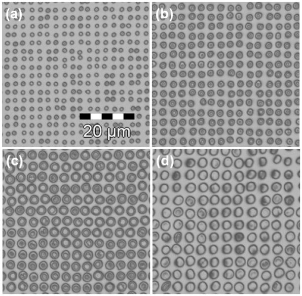
For UVL, PEGDA hydrogel microstructures were fabricated by radical polymerization. To initiate radical polymerization, UV initiator was added with PEGDA polymer. The hydrogel microstructures were designed as disc shapes with diameters from 1 μm to 2.5 μm in 0.5 μm increments for testing the resolution limit and the UV exposure dose required to fabricate the features (figure 4). The exposure dose ranged from 375 mJ/cm2 to 1125 mJ/cm2 in 125 mJ/cm2 increments. The final size of any given hydrogel structure was dose dependent. In particular, for the 1 μm hydrogel structures, hydrogel structures exposed at a dose 1125 μC/cm2 were regularly shaped (figure 4 (a)). However, for the hydrogel structures larger than 1 μm, hydrogel structures at the same exposure dose 1125 μC/cm2 were shaped as biconcave or bioconvex discs due to overexposure and possible over-crosslinking in the different regions (figure 4 (b) – (d)). The resolution of hydrogel microstructures was UV exposure dose dependent, with the final diameters close to the desired diameters when the dose was optimized (Table 2).
Figure 4.
Optical reflection microscopy images of (a) 1 μm, (b) 1.5 μm, (c) 2 μm, and (d) 2.5 μm sizes of dried PEGDA hydrogel microstructures fabricated by UVL with a beam dose of 1125 mJ/cm2.
Table 2.
UV exposure dose for fabrication of different diameter of PEGDA hydrogel microstructures.
| Expected Diameter (μm) | Beam dose (mJ/cm2) | Diameter (nm) |
|---|---|---|
| 1 | 1125 | 1.01 ± 0.048 |
| 1.5 | 625 | 1.61 ± 0.06 |
| 2 | 375 | 1.99 ± 0.10 |
D. Chemical characterization of fabricated hydrogel structures
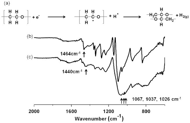
We performed ATR FT-IR to determine the chemical structure of fabricated hydrogel structures. The expected PEG crosslinking mechanisms for both electron beam26 and UV irradiation33 are known. Following electron beam exposure, the spectrum suggests crosslink formation was due to newly formed C-C bonds between PEG polymer backbone chains in the hydrogel (figure 5). The bonds are likely initiated by carbon radicals formed on the PEG backbone during electron beam radiation. The formation of crosslinking between PEG chains in hydrogels affects the mobility of the PEG backbone, as observed by the line broadening. A peak at 1440 cm−1 was observed in hydrogel samples due to the decrease of the frequency of the CH2 vibration. A peak shift from 1464 cm−1 for the CH2 bond in PEG polymer34 is due to the restricted vibration by the network formation in the backbone chain. New peaks at 1067 cm−1, 1037 cm−1 and 1026 cm−1 are proposed to be due to new C-O-C bonds formed after hydrogel formation35.
Figure 5.
(a) Schematic of electron beam radiation crosslinking mechanism in dried PEG film and representative ATR FT-IR spectra (% T) of (b) dried PEG film and (c) PEG hydrogel structures fabricated by EBL at a beam dose of 750 μC/cm2.
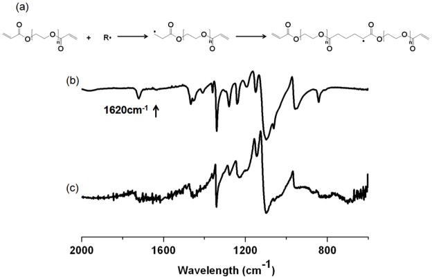
Following UVL (figure 6) the formation of hydrogels from PEGDA is based on UV initiated free radical polymerization of acrylate end groups of PEGDA33. Irgacure 2959, a photoinitiator, dissociates when exposed by UV radiation, creating highly reactive radicals. Formed radicals attack carbon-carbon double bond (-C=C-) of acrylate end groups of PEGDA polymer, initiating free radical polymerization, subsequently creating acrylate networks. The FT-IR spectra of PEGDA polymer film and PEGDA hydrogels were compared to monitor the conversion of PEGDA hydrogel carbon-carbon double bond (-C=C-) to carbon single bond (-C-C-). The double bond at 1620 cm−1 of PEGDA hydrogel spectrum completely disappeared from PEGDA polymer film spectrum as the reaction proceeded, indicating the consumption of -C=C-bonds during crosslinking reaction. The result indicates that PEGDA hydrogels were successfully formed by incorporation of -C=C- bonds.
Figure 6.
(a) Schematic of ultra-violet initiated polymerization mechanism in dried PEGDA film and representative ATR FT-IR spectra (% T) of (b) dried PEGDA film and (c) PEGDA hydrogel structures fabricated by UVL at a beam dose of 1125 mJ/cm2.
E. Hydrogel structure release
In early experiments, UV exposed samples were developed in distilled deionized water. While the samples were developed, adhesion between fabricated hydrogel structures and the silicon wafer was poor and the structures were dispersed easily due to the swelling of crosslinked PEGDA hydrogels. To minimize the dispersal, ethanol was used as a development solvent so that the hydrogel structures swelled less during the development step. The swelling of hydrogels is mainly related with the interaction between the solution and the solute, and ethanol interacts less with hydrogels compared to water because it is less polar than water. The hydrogel structures were imaged with optical microscopy to determine the size of the fabricated hydrogel microstructures
After developing exposed hydrogel films in ethanol, unreacted polymers and initiators were washed away and the patterned hydrogel structures were left on the Si wafer. Sonication for 2 minutes in ethanol was performed to release the hydrogel structures from the Si wafer surface and the hydrogel structures were collected by centrifugation. Dried hydrogel structures, after the centrifugation procedure described previously, were redispersed in 1 mL of distilled deionized water. PEGDA hydrogel microstructures deposited on a glass slide immediately after redispersing in water (figure 7) indicate the promise of hydrogel release from the Si wafer for future applications.
Figure 7.
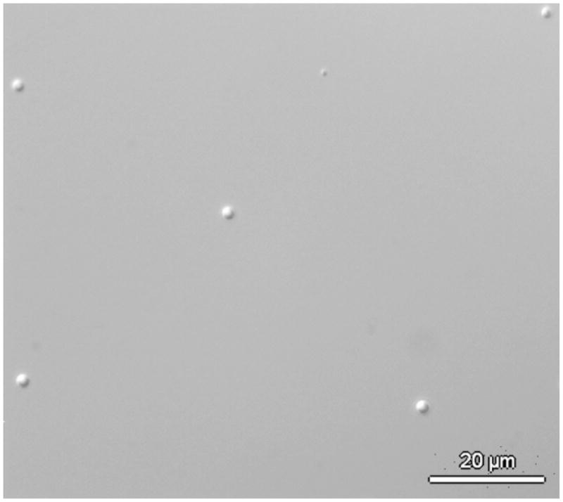
Differential interference contrast micrograph of PEG hydrogel microstuctures formed by UV lithography recovered in ethanol and redisperesed in buffer. The scale bar is 20 μm.
IV. CONCLUSIONS
The EBL and UVL allow fabrication of hydrogel structures in highly-controlled size and shape, thus making them very suitable for pharmaceutical applications. PEG based hydrogel micro- and nanostructures with controlled dimension and shape were successfully fabricated. The network formation by crosslinking between polymer backbone chains was confirmed by FTIR spectroscopy. While EBL provides the smallest hydrogel structures, larger numbers of hydrogel structures can be fabricated in a much shorter time in UVL. From these results, we confirmed the feasibility of synthesizing PEG based hydrogel nano- and microparticles with controlled dimension and shape for biological and biomedical applications. In our future studies, these PEG hydrogel microparticles will be applied for use in a biomolecule delivery platform.
Acknowledgments
This work was conducted in a facility constructed with support from Research Facilities Improvement Program Grant Number C06 RR15482 and supported by grant R01 NS055095 from the NIH. Use of the Center for Nanoscale Materials, Argonne National Laboratory was supported by the U. S. Department of Energy, Office of Science, Office of Basic Energy Sciences, under Contract No. DE-AC02-06CH11357. The first author received the W.C. and May Preble Deiss Award for Biomedical Research from the University of Illinois.
The submitted manuscript has been created by UChicago Argonne, LLC, Operator of Argonne National Laboratory (“Argonne”). Argonne, a U.S. Department of Energy Office of Science laboratory, is operated under Contract No. DE-AC02-06CH11357. The U.S. Government retains for itself, and others acting on its behalf, a paid-up nonexclusive, irrevocable worldwide license in said article to reproduce, prepare derivative works, distribute copies to the public, and perform publicly and display publicly, by or on behalf of the Government.
References
- 1.Thurn K, Brown E, Wu A, Vogt S, Lai B, Maser J, Paunesku T, Woloschak G. Nanoscale Research Letters. 2007;2(9):430–441. doi: 10.1007/s11671-007-9081-5. [DOI] [PMC free article] [PubMed] [Google Scholar]
- 2.Dorian AC, Kevin PH, Joseph MD. Wiley Interdisciplinary Reviews: Nanomedicine and Nanobiotechnology. 2009;1(4):391–404. doi: 10.1002/wnan.40. [DOI] [PMC free article] [PubMed] [Google Scholar]
- 3.Barbé C, Bartlett J, Kong L, Finnie K, Lin HQ, Larkin M, Calleja S, Bush A, Calleja G. Advanced Materials. 2004;16(21):1959–1966. [Google Scholar]
- 4.Goldberg M, Langer R, Jia XQ. J Biomat Sci-Polym E. 2007;18(3):241–268. doi: 10.1163/156856207779996931. [DOI] [PMC free article] [PubMed] [Google Scholar]
- 5.Fessi H, Puisieux F, Devissaguet JP, Ammoury N, Benita S. International Journal of Pharmaceutics. 1989;55(1):R1–R4. [Google Scholar]
- 6.Duncan R. Nat Rev Drug Discov. 2003;2(5):347–360. doi: 10.1038/nrd1088. [DOI] [PubMed] [Google Scholar]
- 7.Kriwet B, Walter E, Kissel T. J Control Release. 1998;56(1–3):149–158. doi: 10.1016/s0168-3659(98)00078-9. [DOI] [PubMed] [Google Scholar]
- 8.McAllister K, Sazani P, Adam M, Cho MJ, Rubinstein M, Samulski RJ, DeSimone JM. J Am Chem Soc. 2002;124(51):15198–15207. doi: 10.1021/ja027759q. [DOI] [PubMed] [Google Scholar]
- 9.Jagielski N, Sharma S, Hombach V, Mailander V, Rasche V, Landfester K. Macromol Chem Physic. 2007;208(19–20):2229–2241. [Google Scholar]
- 10.Nel AE, Madler L, Velegol D, Xia T, Hoek EMV, Somasundaran P, Klaessig F, Castranova V, Thompson M. Nat Mater. 2009;8(7):543–557. doi: 10.1038/nmat2442. [DOI] [PubMed] [Google Scholar]
- 11.Hillaireau H, Couvreur P. Cellular and Molecular Life Sciences. 2009;66(17):2873–2896. doi: 10.1007/s00018-009-0053-z. [DOI] [PMC free article] [PubMed] [Google Scholar]
- 12.Conner SD, Schmid SL. Nature. 2003;422(6927):37–44. doi: 10.1038/nature01451. [DOI] [PubMed] [Google Scholar]
- 13.Tao SL, Desai TA. Advanced Materials. 2005;17(13):1625. [Google Scholar]
- 14.Tao SL, Desai TA. Adv Drug Deliv Rev. 2003;55(3):315–328. doi: 10.1016/s0169-409x(02)00227-2. [DOI] [PubMed] [Google Scholar]
- 15.Truskett VN, Watts MPC. Trends in Biotechnology. 2006;24(7):312–317. doi: 10.1016/j.tibtech.2006.05.005. [DOI] [PubMed] [Google Scholar]
- 16.Rolland JP, Maynor BW, Euliss LE, Exner AE, Denison GM, DeSimone JM. J Am Chem Soc. 2005;127(28):10096–10100. doi: 10.1021/ja051977c. [DOI] [PubMed] [Google Scholar]
- 17.Li HW, Muir BVO, Fichet G, Huck WTS. Langmuir. 2003;19:1963–1965 . [Google Scholar]
- 18.Biswal D, Chirra H, Hilt J. Biomedical Microdevices. 2008;10(2):213–219. doi: 10.1007/s10544-007-9127-6. [DOI] [PubMed] [Google Scholar]
- 19.Xu SQ, Nie ZH, Seo M, Lewis P, Kumacheva E, Stone HA, Garstecki P, Weibel DB, Gitlin I, Whitesides GM. Angew Chem Int Edit. 2005;44(5):724–728. doi: 10.1002/anie.200462226. [DOI] [PubMed] [Google Scholar]
- 20.Euliss LE, DuPont JA, Gratton S, DeSimone J. Chem Soc Rev. 2006;35(11):1095–1104. doi: 10.1039/b600913c. [DOI] [PubMed] [Google Scholar]
- 21.Peppas NA, Bures P, Leobandung W, Ichikawa H. Eur J Pharm Biopharm. 2000;50(1):27–46. doi: 10.1016/s0939-6411(00)00090-4. [DOI] [PubMed] [Google Scholar]
- 22.Peppas NA, Huang Y, Torres-Lugo M, Ward JH, Zhang J. Annu Rev Biomed Eng. 2000;2:9–29. doi: 10.1146/annurev.bioeng.2.1.9. [DOI] [PubMed] [Google Scholar]
- 23.Peppas NA, Keys KB, Torres-Lugo M, Lowman AM. J Control Release. 1999;62(1–2):81–87. doi: 10.1016/s0168-3659(99)00027-9. [DOI] [PubMed] [Google Scholar]
- 24.Euliss LE, Maynor BW, Rolland JP, Desimone JM. Abstr Pap Am Chem S. 2005;230:U4012–U4013. [Google Scholar]
- 25.Gratton SEA, Williams SS, Napier ME, Pohlhaus PD, Zhou ZL, Wiles KB, Maynor BW, Shen C, Olafsen T, Samulski ET, Desimone JM. Accounts Chem Res. 2008;41(12):1685–1695. doi: 10.1021/ar8000348. [DOI] [PMC free article] [PubMed] [Google Scholar]
- 26.Krsko P, Saaem I, Libera M. Stevens Institute of Technology, Chemical, Biomedical and Materials Engineering, presented at the Bioengineering Conference, 2005. Proceedings of the IEEE 31st Annual Northeast, unpublished information; 2005. [Google Scholar]
- 27.Tirumala VR, Divan R, Ocola LE, Mancini DC. J Vac Sci Technol B. 2005;23(6):3124–3128. [Google Scholar]
- 28.Revzin A, Russell RJ, Yadavalli VK, Koh WG, Deister C, Hile DD, Mellott MB, Pishko MV. Langmuir. 2001;17(18):5440–5447. doi: 10.1021/la010075w. [DOI] [PubMed] [Google Scholar]
- 29.Branch DW, Wheeler BC, Brewer GJ, Leckband DE. Biomaterials. 2001;22(10):1035–1047. doi: 10.1016/s0142-9612(00)00343-4. [DOI] [PubMed] [Google Scholar]
- 30.Zhang MQ, Desai T, Ferrari M. Biomaterials. 1998;19(10):953–960. doi: 10.1016/s0142-9612(98)00026-x. [DOI] [PubMed] [Google Scholar]
- 31.Jellison GE. Thin Solid Films. 1996;290–291:40–45. [Google Scholar]
- 32.Keller D. Surface Science. 1991;253(1–3):353–364. [Google Scholar]
- 33.Tan GX, Wang YJ, Li J, Zhang SJ. Polym Bull. 2008;61(1):91–98. [Google Scholar]
- 34.Costa VMD, Fiske TG, Coleman LB. Journal of Chemical Physics. 1994;101 (4):2746–2751. [Google Scholar]
- 35.Silverstein RM, Bassler GC, Morrill TC. Spectrometric identification of organic compounds. 5. Wiley; New York: 1991. [Google Scholar]


