Abstract
Porous silicon nanowire is emerging as an interesting material system due to its unique combination of structural, chemical, electronic, and optical properties. To fully understand their formation mechanism is of great importance for controlling the fundamental physical properties and enabling potential applications. Here we present a systematic study to elucidate the mechanism responsible for the formation of porous silicon nanowires in a two-step silver-assisted electroless chemical etching method. It is shown that silicon nanowire arrays with various porosities can be prepared by varying multiple experimental parameters such as the resistivity of the starting silicon wafer, the concentration of oxidant (H2O2) and the amount of silver catalyst. Our study shows a consistent trend that the porosity increases with the increasing wafer conductivity (dopant concentration) and oxidant (H2O2) concentration. We further demonstrate that silver ions, formed by the oxidation of silver, can diffuse upwards and re-nucleate on the sidewalls of nanowires to initiate new etching pathways to produce porous structure. The elucidation of this fundamental formation mechanism opens a rational pathway to the production of wafer-scale single crystalline porous silicon nanowires with tunable surface areas ranging from 370 m2·g−1 to 30 m2·g−1, and can enable exciting opportunities in catalysis, energy harvesting, conversion, storage, as well as biomedical imaging and therapy.
Keywords: silicon nanowires, porous silicon, electroless chemical etching, surface area, catalysis
INTRODUCTION
Semiconductor nanowires have garnered considerable attention in the past decade due to their unique structural, optical, electronic, mechanical and thermal properties.1–10 Silicon based one-dimensional nanostructures in particular have been intensively studied for nanoscale electronics,11,12 thermoelectrics,13 photovoltaics,14–18 battery electrodes,19–22 and biosensors.23–25 However, silicon nanowire is rarely explored as an active functional material for optoelectronic applications because of its indirect band gap. Interestingly, single crystalline porous silicon nanowires have been recently reported with electrically and optically active properties.26,27,28 In particular, it has been shown that the porous silicon nanowires exhibit visible photoluminescence properties due to the deep quantum confinement effect and/or complex surface states.29 In addition, it has been demonstrated that they can serve as effective photocatalysts for the photocatalytic degradation of organic dyes and toxic pollutants.30 Therefore, combining one-dimensional morphology with porous structure may lead to novel nanostructures, which can potentially cultivate a new class of silicon-based nanoscale optoelectronic and photoelectrochemical devices.31
The reported porous silicon nanowires were produced by one-step or two-step metal-assisted electroless chemical etching approaches.26,27,32 In the one-step etching process, porous silicon nanowires were obtained by immersing highly doped p-type silicon (100) pieces directly into an etching solution containing AgNO3 and HF.26 However, under the same conditions, highly doped n-type silicon (100) substrate is etched predominantly in the lateral direction rather than the vertical direction.27 A two-step metal assisted electroless chemical etching method was employed to grow silicon nanowire arrays from heavily doped n-type silicon substrate.32 The etching process involves chemical deposition of silver metal onto silicon substrate followed by electroless etching in an etchant solution containing H2O2 and HF. Using a similar two-step approach, we have recently reported that, with increasing H2O2 concentration, the resulting silicon nanowires evolve from solid nanowires with smooth surface to rough-surfaced nanowires, then to solid/porous core/shell nanowires and eventually to porous nanowires.27 These studies represent interesting advancements to achieve single crystalline porous silicon nanowires.
It was suggested that the pore originates from the small Ag nanoparticles that nucleate on the sidewalls of nanowires and serve as the etching points for the pore generation.26,27 However, no direct experimental evidence has been given for this argument. Alternative mechanism was also proposed in which metal ions rather than metal nanoparticles was responsible for the pore formation.28 To further elucidate the fundamental mechanism responsible for pore formation and to establish a rational pathway to produce porous silicon nanowires with controllable material parameters for desired functions, here we present a systematic study to investigate the impact of a number of critical experimental parameters that may affect the pore formation during the etching process. These parameters include the dopant concentration of the starting silicon wafer, the H2O2 concentration, and the amount of Ag initially deposited on the silicon substrate.33
We carried out studies on the synthesis of porous silicon nanowires from four different n-type silicon (100) wafers with decreasing resistivities (1–5 Ω·cm, 0.3–0.8 Ω·cm, 0.008–0.016 Ω·cm and 0.001–0.002 Ω·cm) and with variable oxidant (H2O2) concentration ranging from 0.1 M to 0.6 M. Our studies showed that the porosity increases with decreasing the resistivity of the starting wafer and increasing the oxidant (H2O2) concentration. Transmission electron microscope studies clearly show the existence of the silver clusters within the porous silicon nanowires, suggesting that silver particles are responsible for the formation of the porous structure. The clarification of the formation mechanism may open a rational way to produce wafer-scale silicon nanowires with designed porosity, rendering it as a promising material for a wide range of applications.
MATERIALS AND METHODS
Synthesis of Silicon Nanowires
The commercially available silicon wafers with resistivities of 1–5 Ω·cm, 0.3–0.8 Ω·cm, 0.008–0.016 Ω·cm and 0.001–0.002 Ω·cm were used as the starting materials. The pieces of silicon wafers were pre-cleaned with water, acetone and isopropanol. The backside of the silicon pieces was protected by photoresist AZ5214 to avoid etching on the backside. The clean silicon pieces were immersed into a buffered oxide etchant (BOE) to remove the native oxide layer and result in a hydrogen(H)-terminated surface. The H-terminated silicon pieces were coated with Ag by both the solution electroless deposition method described in our previous work27 and the physical vapor deposition approach. Following the Ag deposition, the silicon pieces were placed into an etching solution containing 4.8 M HF and H2O2 of variable concentration (0.1 M, 0.3 M, 0.6 M) for different durations (10, 15, 30 and 60 minutes). After the reaction, the samples were thoroughly washed with a large amount of water and immersed into acetone to remove the photoresist on the backside. When desired, the Ag nanoparticles were removed by soaking the samples into concentrated nitric acid for approximately one hour. Finally, the silicon pieces were rinsed with water several times and dried with nitrogen flow. A systematic study was carried out to investigate the effect of the resistivity of the starting wafer, the oxidizer concentration, the amount of Ag and the etching duration on the formation of the porous nanowires. A list of experimental variables and key results are summarized in Table 1 and 2.
Table 1.
A summary of experimental variables and key results for investigating the effects of oxidizer concentration and the starting wafer resistivity on the pore formation. Ag was chemically deposited on the silicon wafer. The nanowires were obtained by immersing the Ag coated silicon wafer in an etching solution containing 4.8 M HF and H2O2 of variable concentration for 30 minutes.
| The resistivity of starting silicon wafer | ||||
|---|---|---|---|---|
| 1–5 Ω·cm | 0.3–0.8 Ω·cm | 0.008–0.016 Ω·cm | 0.001–0.002 Ω·cm | |
| 0.1 M H2O2 | Solid nanowires Length: 5.9 µm |
Solid nanowires Length: 6.9 µm |
Solid nanowires Length: 7.1 µm |
Solid/porous coreshell nanowires Length: 3.5 µm |
| 0.3 M H2O2 | Rough surface nanowires Length: 17.1 µm |
Rough surface nanowires Length: 21.0 µm |
Solid/porous coreshell nanowires Length: 21.5 µm |
Porous nanowires Length: 18.1 µm |
| 0.6 M H2O2 | Rough surface nanowires Length: 25.0 µm |
Rough surface nanowires Length: 26.0 µm |
Porous nanowires Length: 29.3 µm |
Porous nanowire Length: 19.4 µm |
Table 2.
Experimental parameters used for investigating the effect of the resistivity of the starting wafer and reaction duration on the length of nanowires. A 20 nm thick Ag film was physically evaporated on the silicon wafer as the etching metal. The concentration of H2O2 was kept at 0.3 M.
| The resistivity of starting silicon wafer | ||||
|---|---|---|---|---|
| 1–5 Ω·cm | 0.3–0.8 Ω·cm | 0.008–0.016 Ω·cm | 0.001–0.002 Ω·cm | |
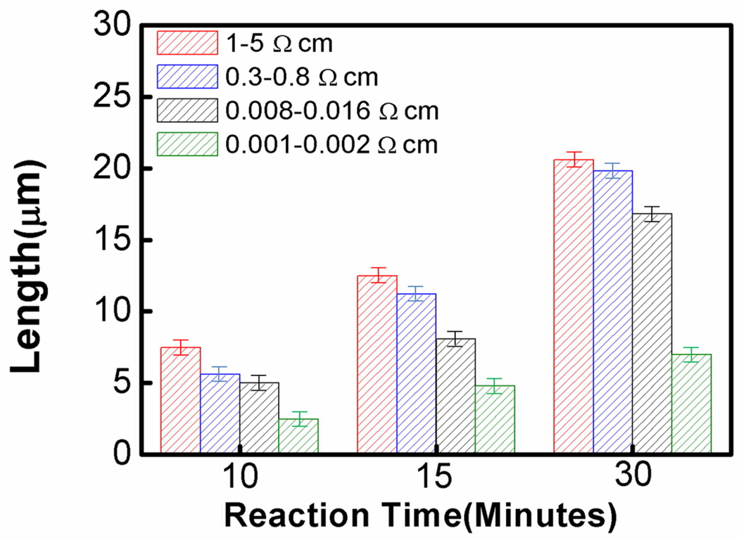
| 10 Minutes | Length: 7.5 um | Length: 5.6 um | Length: 5 um | Length: 2.5 um |
| 15 Minutes | Length: 12.5 um | Length: 11.2 um | Length: 8.1 um | Length: 4.8 um |
| 30 Minutes | Length: 20.6 um | Length: 19.8 um | Length: 16.8 um | Length: 7.0 um |
Characterization of Silicon Nanowires
The as-synthesized silicon nanowires were characterized by scanning electron microscopy (SEM JEOL 6700) and transmission electron microscopy (TEM, CM120). The high resolution TEM (HRTEM) and selected area electron diffraction (SAED) were obtained on FEI Titan with an operation voltage of 300 kV.
The surface area was determined by the Brunauer-Emmett-Teller (BET) method using an Autosorb-1 (Quantachrome) volumetric analyzer at 77 K using a liquid nitrogen bath. The samples (approximately 15 mg) were scratched from the wafers and degassed overnight at 250 °C before the BET measurements. An ultra-high purity (UHP, 99.999% purity) grade of N2 and He gases were used throughout the adsorption experiments. The BET surface areas were determined by using the data under the relative pressures between 0.05 and 0.25 before the capillary condensation. The pore size distributions were calculated from the adsorption data by the Barret-Joyner-Halenda (BJH) method.
RESULTS AND DISCUSSION
It is helpful to note that for the four types of wafers used (1–5 Ω·cm, 0.3–0.8 Ω·cm, 0.008–0.016 Ω·cm and 0.001–0.002 Ω·cm), the dopant concentrations are roughly 1015/cm3, 1016/cm3, 1018/cm3, and 5×10¹⁹/cm3, which corresponds to a single dopant atom per cube with an edge length of 100 nm, 50 nm, 10 nm and 3 nm, respectively. A systematic study was first carried out to investigate the effects of the starting wafer resistivity and the oxidizer concentration on the pore formation. For discussion purposes, we divided four types of wafers into two groups in terms of dopant concentrations (lightly doped: 1–5 Ω·cm and 0.3–0.8 Ω·cm; highly doped: 0.008–0.016 Ω·cm and 0.001–0.002 Ω·cm). A list of experimental variables and key results are summarized in Table 1.
Silicon Nanowire Arrays Based on Lightly Doped n-Si (100) Wafers (1–5 and 0.3–0.8 Ω·cm)
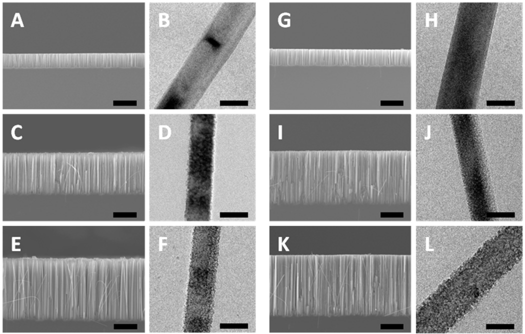
Figure 1A, 1C, and 1E display the cross sectional SEM images of silicon nanowire arrays (1–5 Ω·cm) obtained with various H2O2 concentrations of 0.1 M, 0.3 M and 0.6 M, respectively. SEM images show uniform vertical arrays of silicon nanowires on the substrate. As expected, the length of silicon nanowires becomes longer with increasing H2O2 concentration. Figure 1B, 1D, and 1F show the TEM images of the silicon nanowires obtained from 1–5 Ω·cm wafer with H2O2 concentration of 0.1 M, 0.3 M and 0.6 M, respectively. At a low concentration of H2O2 (0.1 M), the silicon nanowires are non-porous with smooth surfaces. With increasing concentration of H2O2, the surfaces of the silicon nanowires become rough as shown in Figure 1D (0.3 M) and 1F (0.6 M). No obvious pores are observed.
Figure 1.
TEM and SEM images of the silicon nanowires obtained from 1–5 and 0.3–0.8 Ω·cm n-type Si (100) wafer in etchant solutions composed of 4.8 M HF and H2O2 of variable concentrations through a two-step reaction for 30 minutes. (A,B) Nanowires formed from 1–5 Ω·cm silicon wafer with 0.1 M H2O2. (C,D) Nanowires formed from 1–5 Ω·cm silicon wafer with 0.3 M H2O2. (E,F) Nanowires formed from 1–5 Ω·cm silicon wafer with 0.6 M H2O2. (G,H) Nanowires formed from 0.3–0.8 Ω·cm silicon wafer with 0.1 M H2O2. (I,J) Nanowires formed from 0.3–0.8 Ω·cm silicon wafer with 0.3 M H2O2. (K,L) Nanowires formed from 0.3–0.8 Ω·cm silicon wafer with 0.6M H2O2. The scale bars in all SEM and TEM images are 10 µm and 100 nm, respectively.
Figure 1G, 1I, and 1K show the cross sectional SEM images of the silicon nanowire arrays obtained from the silicon wafer with a resistivity of 0.3–0.8 Ω·cm. The results show a similar trend to those synthesized from 1–5 Ω·cm silicon wafer. The higher the concentration of H2O2, the longer the length of the silicon nanowires is. Representative TEM images are shown in Figure 1H, 1J and 1L for 0.1 M, 0.3 M and 0.6 M H2O2, respectively. Similar morphologies of silicon nanowires are observed compared to the nanowires from 1–5 Ω·cm wafer, with no clear evidence of pore formation either.
Silicon Nanowire Arrays Synthesized from Highly Doped n-Si(100) Wafers (0.008–0.016 and 0.001–0.002 Ω·cm)
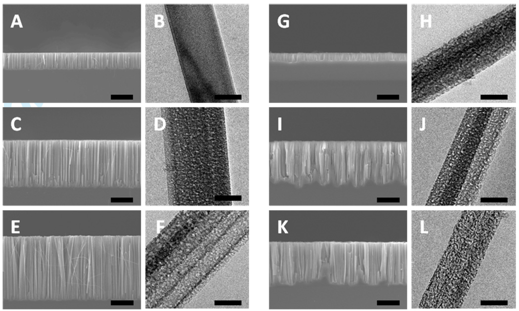
The SEM images of the cross sections are shown in Figure 2A, 2C, 2E for silicon nanowire arrays obtained from 0.008–0.016 Ω·cm silicon wafer. Similar to the etching behaviors of the lightly doped silicon wafers, the nanowire length increases from 7.1 µm (Figure 2A) to 29.3 µm (Figure 2E) with increasing H2O2 concentration. Representative TEM images of each sample are shown in Figure 2B, 2D and 2F. For H2O2 concentration of 0.1 M, non-porous silicon nanowires are obtained. However, a porous structure is observed when the concentration of the H2O2 reaches 0.3 M. As the concentration of H2O2 is further increased to 0.6 M, the porosity of nanowires also increases.
Figure 2.
TEM and SEM images of the silicon nanowires obtained from 0.008–0.016 Ω·cm and 0.001–0.002 Ω·cm n-type Si (100) wafers in etchant solutions composed of 4.8 M HF and H2O2 of variable concentrations through a two-step reaction for 30 minutes. (A,B) Nanowires formed from 0.008–0.016 Ω·cm silicon wafer with 0.1 M H2O2. (C,D) Nanowires formed from 0.008–0.016 Ω·cm silicon wafer with 0.3 M H2O2. (E,F) Nanowires formed from 0.008–0.016 Ω·cm silicon wafer with 0.6 M H2O2. (G,H) Nanowires formed from 0.001–0.002 Ω·cm silicon wafer with 0.1 M H2O2. (I,J) Nanowires formed from 0.001–0.002 Ω·cm silicon wafer with 0.3 M H2O2. (K,L) Nanowires formed from 0.001–0.002 Ω·cm silicon wafer with 0.6 M H2O2. The scale bars for all SEM and TEM images are 10 µm and 100nm, respectively.
Figure 2H, 2J, and 2L are TEM images for silicon nanowires synthesized from 0.001–0.002 Ω·cm silicon wafer with increasing H2O2 concentrations. Notably, at H2O2 concentration of 0.1 M, pores are already observed on the surfaces of silicon nanowires. With increasing H2O2 concentration, the porosity of silicon nanowires increases significantly. Longer nanowires are produced with increasing H2O2 concentration as shown in the cross sectional SEM images (Figure 2G, 2I, and 2K).
It is now well accepted that the silicon nanowires are formed through Ag particle catalyzed electroless etching. The total reaction is: 32
| (1) |
For the same type of silicon wafer, according to the Nernst equation which characterizes the etching process: 27
| (2) |
The etching rate is expected to increase with increasing H2O2 concentration which explains why longer nanowires are obtained with a higher H2O2 concentration. During the etching process, Ag nanoparticles at the roots of the nanowires can be converted into Ag+ ions by H2O2.27 At a low H2O2 concentration, the generated Ag+ ions can be recovered back to Ag by taking electrons from silicon. A higher H2O2 concentration will lead to a higher concentration of the Ag+ ions, which may have more chances to diffuse up and re-nucleate on the sidewalls of the silicon nanowires to form new etching sites. As a result, surface roughness and porosity are achieved for lightly and highly doped wafers at high H2O2 concentration.
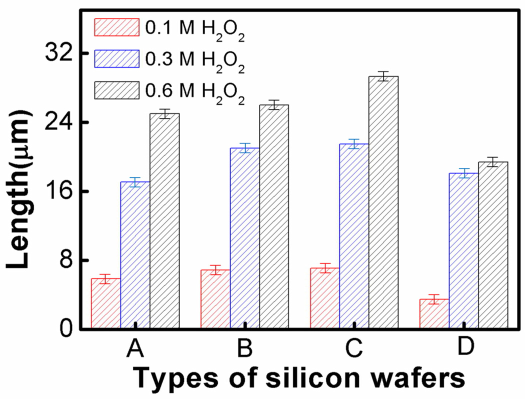
The above discussions clearly illustrate the role of H2O2 in the etching process. A summary of the nanowire length evolution as the function of H2O2 concentration for four types of silicon wafers is presented in Figure 3. Longer nanowires are generally obtained at higher H2O2 concentration while other conditions are kept the same. It is consistent with the expected increase in vertical etching rate with increasing H2O2 concentration. The impact of dopant concentration is much more complicated: even though the surface roughness or porosity increases with increasing dopant concentration, a monotonic trend in the nanowire length vs dopant concentration is not observed. For example, with the increase of the dopant concentration of the silicon wafer, an increase in the nanowire length is firstly observed followed by an unexpected decrease at a very high dopant concentration (e.g. 0.001–0.002 Ω·cm). This non-monotonic dependence on the dopant concentration suggests there are other competing factors that can impact the vertical etching rate.
Figure 3.
Length evolution of silicon nanowires from four types of starting wafers with increasing H2O2 concentration. (A) Silicon nanowires from 1–5 Ω·cm silicon wafer. (B) Silicon nanowires from 0.3–0.8 Ω·cm silicon wafer (C) Silicon nanowires from 0.008–0.016 Ω·cm silicon wafer (D) Silicon nanowires from 0.001–0.002 Ω·cm silicon wafer.
We have shown that the amount of Ag initially deposited on the silicon substrate is dependent on the dopant concentration (See Supporting Information Figure S1).27 We hypothesized and confirmed that the amount of Ag can significantly affect the etching rate (See Supporting Information Figure S2). To remove this variable of Ag amount, we designed a second set of experiments by using evaporated Ag film as the starting etching metals. By physically depositing 20 nm Ag, four types of wafers with equal amounts of Ag were used for the growth of silicon nanowires under the same experimental conditions. When exposed to the etching solution for a short period of time, the deposited Ag film forms isolated islands (See Supporting Information Figure S3).
Figure 4 displays the TEM images of nanowires from four types of wafers etched for 15 minutes in 0.3 M H2O2 etchant solution, showing similar results to those obtained with chemical deposition silver. Nanowires from two lightly doped wafers only show surface roughness while nanowires from two highly doped wafers show increasing porosity with the increase of dopant concentration.
Figure 4.
TEM images of the silicon nanowires obtained from four types of wafers with e-beam evaporation deposited Ag-film as the etching metal in etchant solutions composed of 4.8 M HF and 0.3 M H2O2 through a two-step reaction for 15 minutes. (A) Silicon nanowires from 1–5 Ω·cm wafer. (B) Silicon nanowires from 0.3–0.8 Ω·cm wafer. (C) Silicon nanowires from 0.008–0.016 Ω·cm wafer. (D) Silicon nanowires from 0.001–0.002 Ω·cm wafer. The scale bars are 100 nm.
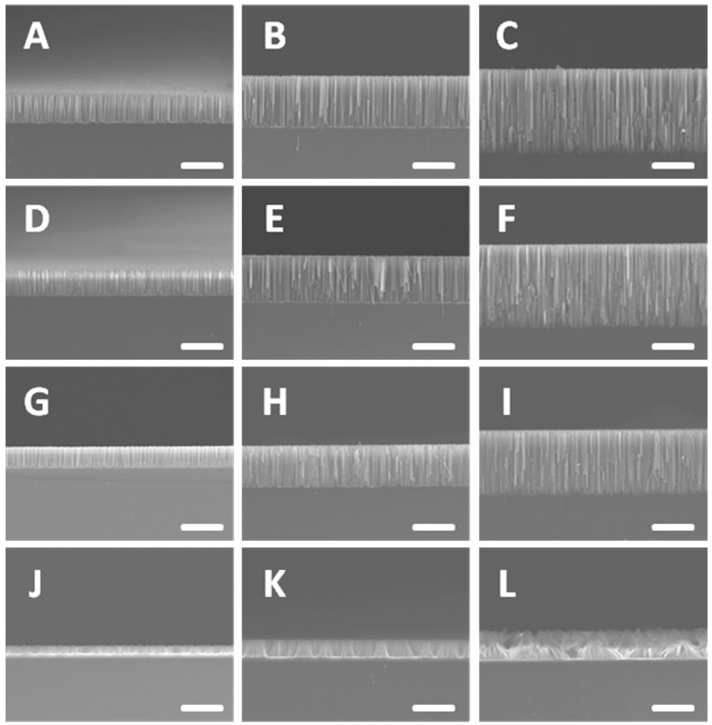
Figure 5 shows the cross sectional SEM images of the nanowires obtained from four types of wafers with physical vapor deposited Ag-films and variable reaction durations. A list of the key experimental parameters and length of the resulting nanowires were summarized in Table 2. The summary of length evolution as a function of etching time is also displayed in Figure 6. Surprisingly, the length of the nanowires becomes consistently shorter with increasing dopant concentration. In other words, the vertical etching rate decreases with increasing dopant concentration. This trend is particularly evident in the case of nanowires obtained from highly doped silicon wafer. This observation appears to be in contradiction with the conventional wisdom that the etching rate should increase with increasing dopant concentration. Nonetheless, this phenomenon can be fully explained after we reconsider the etching process more carefully. According to the assumed mechanism27, the initially deposited Ag nanoparticles at the roots of the silicon nanowires can be oxidized by H2O2 to form Ag+ ions, which may diffuse out and re-nucleate around the defective sites (e.g. near dopants) on the nanowires sidewalls. Consequently, the more the Ag clusters nucleate on the sidewall, the less the Ag is left at the nanowire roots, and the slower the etching rate is along the vertical direction. As higher degree of porosity is observed in nanowires from higher dopant concentration wafers, we believe that the amount of Ag that dissolves and diffuses up is positively correlated with the dopant concentration.
Figure 5.
SEM images of nanowires evolved from four types of wafers with deposited Ag-film for various reaction times in the etchant solutions containing 0.3 M H2O2. (A–C) Silicon nanowires from 1–5 Ω·cm wafer for reaction times of 10 minutes, 15 minutes and 30 minutes, respectively. (D–F) Silicon nanowires from 0.3–0.8 Ω·cm wafer for reaction times of 10 minutes, 15 minutes and 30 minutes, respectively. (G–I) Silicon nanowires from 0.008–0.016 Ω·cm wafer for reaction times of 10 minutes, 15 minutes and 30 minutes, respectively. (J–L) Silicon nanowires from 0.001–0.002 Ω·cm wafer for reaction times of 10 minutes, 15 minutes and 30 minutes, respectively. The scale bars are 10 µm.
Figure 6.
Length evolution of silicon nanowires obtained from four types of wafers with physical vapor deposited Ag-film as a function of reaction time. Red: silicon nanowires from 1–5 Ω·cm wafer. Blue: silicon nanowires from 0.3–0.8 Ω·cm wafer. Black: silicon nanowires from 0.008–0.016 Ω·cm wafer. Green: silicon nanowires from 0.001–0.002 Ω·cm wafer.
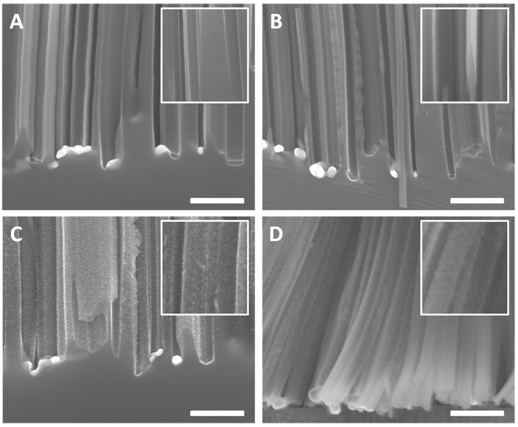
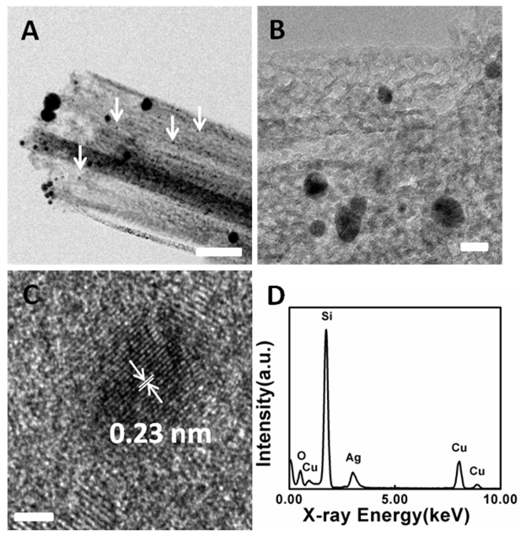
In order to further probe the etching process and achieve solid experimental evidences of the assumed mechanism27, we have studied cross sectional SEM images of nanowires obtained from four types of wafers with physical vapor deposited Ag-film before removing Ag. As expected, the nanowires from two lightly doped wafers (Figure 7A, 7B) show relatively clean and smooth surfaces. In contrast, nanowires from two highly doped wafers (Figure 7C, 7D) show rough surfaces with a large number of specks that may be attributed to re-nucleated Ag nanoclusters. Most of these specks disappeared after immersing the nanowires in the nitric acid for one hour, suggesting that these specks are small Ag nanoparticles (See Supporting Information Figure S4). TEM studies of these nanowires before removing Ag further show that a large number of Ag nanoclusters are present on or in the porous nanowires (Figure 8A, 8B). The sizes of Ag nanoclusters exhibit a broad distribution with the majority in a few nanometer regime and a few larger ones. The large particles may come from the roots during the TEM sample preparation steps. HRTEM and element analysis by EDX were carried out to confirm that these nanoclusters are indeed Ag (Figure 8C, 8D).
Figure 7.
Cross sectional SEM image of nanowires evolved from four types wafers with reaction time of 15 minutes in the etchant solutions containing 0.3 M H2O2 without immersing in the nitric acid solution. The insets are enlarged SEM images for each type of the nanowires respectively. (A) Silicon nanowires from 1–5 Ω·cm wafer. (B) Silicon nanowires from 0.3–0.8 Ω·cm wafer. (C) Silicon nanowires from 0.008–0.016 Ω·cm wafer. (D) Silicon nanowires from 0.001–0.002 Ω·cm wafer. The scale bars are 500 nm.
Figure 8.
(A,B) TEM images of a porous silicon nanowire decorated with Ag nanoparticles on the sidewall. The silicon nanowire was made from 0.008–0.016 Ω·cm silicon wafer in 0.3 M H2O2 for 15 minutes without the treatment in the concentrated nitric acid. Small Ag nanoparticles are indicated by the white arrows. The scale bars are 80 nm and 20 nm for 8A and 8B, respectively. (C) HRTEM of Ag nanoparticles on the sidewall of the porous silicon nanowire. The lattice spacing 0.23 nm corresponds to Ag (111) plane. The scale bar is 2 nm. (D) An EDX spectrum recorded from one nanowire. Ag was detected on the nanowire, confirming the TEM characterization.
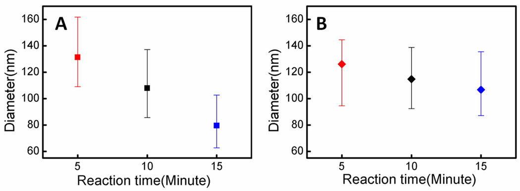
The etching dynamics can also be probed by analyzing the size of catalytic Ag nanoparticles at the nanowire roots. Although the size distribution of the Ag nanoparticles can be quite broad, a careful statistical analysis of the size evolution of the Ag nanoparticles can still reveal a consistent trend. For reactions on highly doped wafers, the sizes of Ag nanoparticles at the roots reduce significantly with increasing reaction time (Figure 9A). This can be attributed to the partial dissolution of Ag nanoparticles at the roots into Ag+ ions, upward diffusion of Ag+ ions, and re-nucleation of Ag clusters on nanowire sidewalls. For reactions on lightly doped wafers, a much smaller decrease in the size of Ag nanoparticles is observed (Figure 9B) due to the less consumption of Ag+ through re-nucleation process on the sidewalls.
Figure 9.
Size distribution of Ag nanoparticles at the roots of the nanowires with increasing reaction time. (A) Reactions on 0.008–0.016 Ω·cm silicon wafer. (B) Reactions on 1–5 Ω·cm silicon wafer.
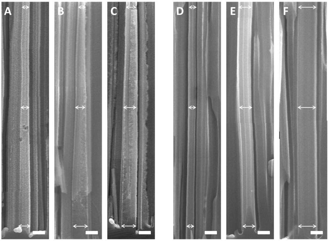
A further evidence of the size shrinking of the Ag nanoparticles at the roots is the trapezoid structure observed in nanowires obtained from highly doped silicon wafers (Figure 10A–C). The images clearly show that diameter near the tip is smaller than that near the root, indicating the fact that the size of Ag nanoparticles is decreasing as the reaction proceeds. On the other hand, nanowires from lightly doped wafers (Figure 10D–F) kept nearly the same width (diameter), suggesting that the size of the Ag nanoparticles is not significantly changed throughout the reaction process.
Figure 10.
(A–C) Cross sectional SEM images of nanowires from 0.008–0.016 Ω·cm silicon wafer etched in 0.3 M H2O2 for 15 mintues, showing the trapezoid structure. The diameter of the upper part is smaller than the lower part, indicating the size of Ag nanoparticle is shrinking as the reaction proceeds. (D–F) Cross sectional SEM images of nanowires from 0.3–0.8 Ω·cm silicon wafer etched in 0.3 M H2O2 for 15 mintues, showing nearly constant wire width/diameter, suggesting that the size of Ag nanoparticles remains nearly unchanged in the etching process. The images are grouped together from multiple images to show the diameter/width evolution over extended length. The scale bars are 200 nm.
Based on the experimental results discussed above, we can draw several solid conclusions in the following three aspects and propose an optimal model to elucidate the fundamental mechanism for the formation of the porous silicon nanowires.
The Effect of H2O2 Concentrations on the Etching Rate and the Pore Formation. With increasing H2O2 concentration, the vertical etching rate increases, resulting in longer nanowires. Additionally, H2O2 concentration can be used as a tuning factor to control the surface roughness and the overall porosity of the resulting silicon nanowires.
The Effect of the Silicon Wafer Dopant Concentration on the Surface Roughness and Pore Formation. The dopant concentration of the wafer is one of the key factors that determine whether a porous structure or a non-porous structure with a rough surface can be achieved. The overall vertical etching rate is inversely associated with the dopant concentration of the starting wafer if the amount of Ag is kept the same at the beginning of the reaction.
The Role of Ag Initially Deposited On the Silicon Wafer. Ag initially deposited on the silicon wafer will serve both as the cathode and the catalyst in the etching process.34 As the catalyst, Ag at the roots may dissolve, diffuse upwards and re-nucleate on the defective sites on the sidewalls of the silicon nanowires. For highly doped wafers with more defective sites (e.g. near dopants), more Ag nanoclusters may therefore form on nanowires and function as new etching points for the formation of pores; while for lightly doped wafer with fewer dopant sites, fewer Ag nanoclusters may form on the nanowires and it is therefore less likely to form porous structures.
Illustration of the Proposed Mechanism for the Formation of Porous Nanowires
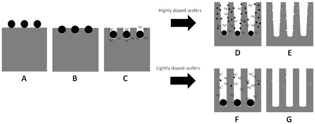
Scheme 1 is a schematic summary of the etching model for the formation of porous and non-porous nanowires from highly and lightly doped wafers. In the two-step etching method, Ag nanoparticles are firstly deposited on the surface of the silicon wafer (Scheme 1A). When the etching process is initiated (Scheme 1B), the nanoparticles serve as a cathode while the silicon serves as an anode to form an electrochemical cell. The half cell reactions are as follows:33,35
- Anode (Si):
(3) - Cathode (Ag):
(4)
Scheme 1.
Schematic illustrations of the formation process of porous and non-porous silicon nanowire arrays through a two-step silver assisted etching method from the highly and lightly doped wafers respectively.
At the anode, the silicon is continuously dissolved by electron transferring to the upper surfaces of the Ag nanoparticles to reduce H2O2 into H2O. While serving as a cathode, Ag nanoparticles can also be oxidized into Ag+ ions by H2O2 according to the following reaction:
| (5) |
On the other hand, these Ag+ ions can be quickly reduced back to Ag by taking electrons at the interface of Ag and Si before they can diffuse out. The reaction is:
| (6) |
As a result, the Ag+ ions are confined in the close proximity of the Ag nanoparticles (Scheme 1C). In this way the Ag nanoparticles are confined in the nanopits that they create and the silicon below the Ag nanoparticles is continuously etched down to form the silicon nanowires. In general, the concentration of the Ag+ ions is expected to increase with increasing the H2O2 concentration, and part of the Ag+ ions can diffuse upwards from the roots and re-nucleate on the sidewalls of the nanowires. Those newly nucleated Ag nanoclusters can serve as the new etching sites which may lead to the pore formation on the nanowires sidewalls.
Generally, a higher dopant concentration of the silicon wafer would result in a higher silicon etching rate due to the larger number of defective sites near dopants that are favorable for the etching process. On the other hand, since the defective sites are preferred nucleation sites for Ag+ ions, there would be a larger number of Ag nanoclusters formed on the sidewalls of the silicon nanowires from highly doped wafers (Scheme 1D). With Ag nanoclusters continuously nucleating on the sidewalls of the nanowires, the equilibrium of reaction (5) can’t be reached. More Ag at the roots will dissolve and diffuse upwards to compensate the decreasing Ag+ concentration in the solution. As a result, the amount of the Ag at the roots of the nanowires from highly doped wafers decreases gradually, which slows down the vertical etching rate. On the contrary, the nanowires from lightly doped silicon wafers have few defective sites on surface so that there is less chance for Ag+ to nucleate on the sidewalls (Scheme 1F). Therefore, the concentration of Ag+ ions remains nearly constant. The amount of Ag at roots is fixed and becomes more than that in highly doped wafers as reaction proceeds. Thus, the vertical etching of silicon nanowires from lightly doped wafers can maintain at a stable rate and surpasses that from the highly doped ones.
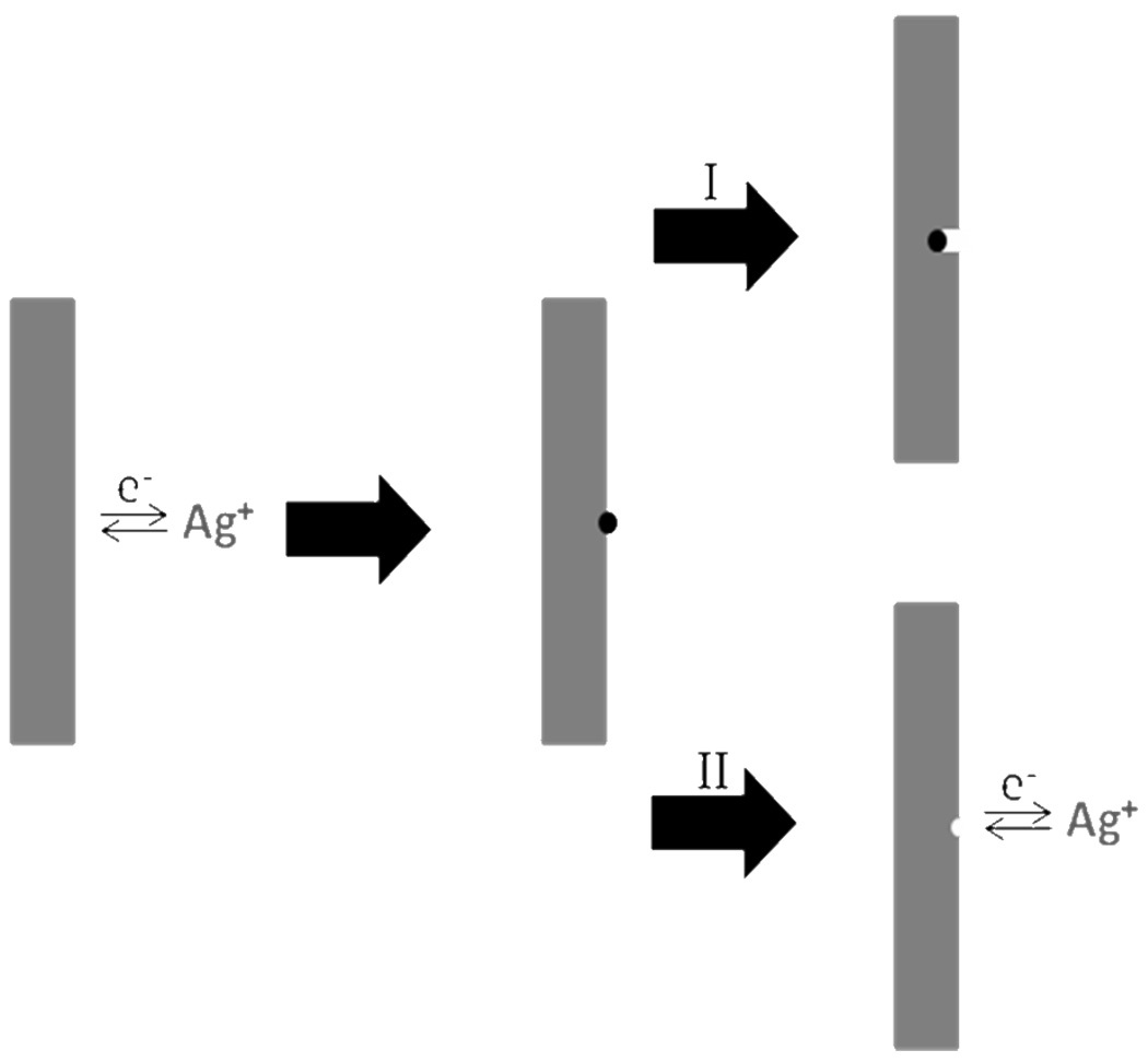
The dissolution and nucleation of Ag nanoparticles on silicon nanowires is a highly dynamic process and closely related to the silicon etching process. According to the reaction (5), the dissolving rate of the Ag is only related to the concentration of the [H+] and [H2O2]. Hence for any type of silicon wafers, the dissolving rate of Ag is nearly identical under the same reaction conditions, regardless of the dopant concentration. The nucleation of Ag, however, is strongly related to the etching rate and hence the dopant concentration of the silicon wafer. Our studies clearly suggest that a higher dopant concentration can lead to more effective Ag nucleation (See Supporting Information Figure S1). Therefore, for highly doped silicon wafers, the larger number of dopant defects (e.g. ~1 dopant per cube with a edge length of 3 nm for 0.001–0.002 Ω·cm wafer) can lead to a higher silicon etching rate to facilitate the nucleation of Ag nanoparticles on the nanowire sidewalls and sustain them to function as effective etching sites for the formation of pores (Scheme 2-I). In contrast, for the lightly doped silicon, only a small number of Ag clusters may nucleate on the nanowire sidewalls due to a small number of defects (e.g. one dopant per cube with a edge length of 100 nm for 1–5 Ω·cm wafer). Additionally, the slow silicon etching rate may not be sufficient to sustain the small Ag clusters in the stable format and the Ag clusters may be readily converted back to Ag+ ions by H2O2 (Scheme 2-II). In this case, the Ag clusters may not be able to serve as effective etching sites or only etch a small portion of the nanowire surface to result in rough surfaced nanowires.
Scheme 2.
Schematic illustration of the two possible behaviors of the anchored Ag nanoparticles on the sidewalls of silicon nanowires. I. The anchored Ag nanoparticle acted as a new etching site. II. The anchored Ag nanoparticle re-dissolved into solution.
Our proposed mechanism is consistent with the explanation of pore formation in one step method, 26 in which the Ag+ ions nucleating on the surface of the nanowires come from the original solution rather than from the oxidation of the Ag nanoparticles at the roots of the nanowires. A recent study suggested the pore formation mechanism of the two step etching and attributed the etching on the surface of the nanowires to the Ag+ ions in the solution since no Ag nanoparticles were observed in their experiment.28 In our studies, SEM and TEM images clearly show small Ag nanoparticles in/on the resulted porous nanowires, which supports the argument for our experiment. Nonetheless, considering the dissolution and nucleation of the Ag is a highly dynamic process, the Ag nanoparticles may be quickly converted into Ag+ ions and may not be readily observable under certain experimental conditions.
Control of Porosity and Specific Surface Area of the Porous Silicon Nanowires
With high porosity and high specific surface area, such porous nanowires show considerable promise in catalysis, separation, hydrogen adsorption, and energy storage. For example, mesoporous Co3O4 nanowire arrays were found to good candidates for lithium ion batteries with high capacity and rate capability.36 Porous platinum nanowire arrays showed enhanced electrocatalytic activities for ethanol oxidation in direct alcohol fuel cells. 37
Our systematic studies readily allow us to tune the porosity and specific surface area of the nanowires. The standard multipoint BET analysis was performed to determine the porosity and specific surface area of the porous and non-porous nanowires obtained with various silicon wafers or etching conditions. Nitrogen adsorption/desorption isotherms for different silicon nanowires are shown in Figure 11A. For the reaction time of 30 minutes in an etching solution of 0.3 M H2O2 and 4.8 M HF, porous silicon nanowires obtained from 0.008–0.016 Ω·cm silicon wafer show a surface area of 240 m2·g−1 ,while porous silicon nanowires obtained from 0.001–0.002 Ω·cm silicon wafer show a significant increase of the surface area to 370 m2·g−1. For non-porous silicon nanowires obtained from 1–5 Ω·cm and 0.3–0.8 Ω·cm silicon wafers, surface areas are 30 m2·g−1 and 40 m2·g−1, respectively. The total pore volumes are 0.65 cm3/g, 0.47 cm3/g, 0.06 cm3/g and 0.05 cm3/g at P/Po = 0.90 for silicon nanowires obtained from wafers with the resistivities of 0.001–0.002 Ω·cm, 0.008–0.016 Ω·cm, 0.3–0.8 Ω·cm and 1–5 Ω·cm, respectively. The results clearly demonstrate that higher dopant concentration of the starting silicon wafer leads to more porosity in silicon nanowires.
Figure 11.
(A) Nitrogen adsorption/desorption isotherms of porous and nonporous silicon nanowires obtained from wafers with various resistivities. The mean BET surface areas of the different nanowires are 370 m2·g−1, 240 m2·g−1, 40 m2·g−1 and 30 m2·g−1, respectively. (B) Nitrogen adsorption/desorption isotherms of porous nanowires obtained from 0.08–0.016 Ω·cm wafer with various reaction time. (C) Corresponding BJH pore size distributions for of different nanowires. The mean pore diameters are 10.0 nm and 9.7 nm for porous silicon nanowires obtained from 0.001 Ω·cm and 0.08–0.016 Ω·cm silicon wafers, respectively.
Figure 11B shows the nitrogen adsorption/desorption isotherms for the silicon nanowires obtained from the silicon wafer (0.008–0.016 Ω·cm) with various reaction times. As expected, the surface area increases with increasing the reaction time. For the reaction time of 15 minutes, 30 minutes and 60 minutes, the surface areas were 160 m2·g−1, 240 m2·g−1 and 337 m2·g−1, respectively.
Figure 11C shows the typical pore size distribution for the porous/non-porous nanowires calculated by the BJH model. The pore distribution of silicon nanowires synthesized from lightly doped wafers is flat over the entire range, indicating the lack of pores. On the other hand, the mean pore diameters of the porous nanowires are 10.0 nm and 9.7 nm for silicon nanowires synthesized from the silicon wafers with resistivities of 0.001–0.002 Ω·cm and 0.008–0.016 Ω·cm, respectively.
HRTEM studies were also used to study the crystalline structure and directly image the pore structures. In general, the porous silicon nanowires retain the single crystalline structure of the original silicon wafers. Figures 12A and 12B show HRTEM images of porous nanowires obtained from 0.08–0.016 Ω·cm and 0.001–0.002 Ω·cm silicon wafers by etching in solution containing 0.3 M H2O2 and 4.8 M HF for 15 minutes, respectively. The insets are fast Fourier transform (FFT) patterns of the corresponding lattice-resolved HRTEM images. These FFT patterns combined with crystal lattice images indicate that the axial direction of the nanowires is [100]. Figure 12C shows the HRTEM image of the porous nanowire obtained from 0.001–0.002 Ω·cm silicon wafer by etching in 0.6 M H2O2 and 4.8 M HF for 15 minutes. The silicon nanowires become so porous that it forms a network with narrow walls of 2–3 nm. The HRTEM studies also show that pores typically have a size around 10 nm, which is consistent with BET studies.
Figure 12.
HRTEM images with FFT of porous silicon nanowires. (A) Nanowires obtained from 0.008–0.016 Ω·cm silicon wafer in the etching solution of 0.3 M H2O2 and 4.8 M HF for 15 minutes. (B) Nanowires obtained from 0.001–0.002 Ω·cm silicon wafer in the etching solution of 0.3 M H2O2 and 4.8 M HF for 30 minutes. (C) Nanowires obtained from 0.001–0.002 Ω·cm silicon wafer in the etching solution of 0.6 M H2O2 and 4.8 M HF for 15 minutes. The scale bars are 2 nm.
CONCLUSIONS
In conclusion, we have presented a systematic study on the synthesis of porous silicon nanowires through the two-step metal assisted wet-etching method and revealed the fundamental mechanism for the formation of the porous silicon nanowires. Large scale single crystalline porous silicon nanowire arrays were synthesized in a highly controlled manner by systematically tuning the dopant concentration of the starting silicon wafers and the concentration of the H2O2. Our studies showed that the Ag metal at the roots of the nanowires can be converted into Ag+ and re-nucleate on the sidewalls of the nanowires. The presence of a large amount of defective sites in highly doped silicon wafers (e.g 5×10¹⁹/cm3 for 0.001–0.002 Ω·cm) allows more Ag nanoclusters to form on the sidewalls of the nanowires, developing new etching sites to eventually create porous structure with a surface area as high as 370 m2·g−1. The availability to synthesize large-scale single crystalline porous silicon nanowires with predictable and controllable porosity can open up exciting opportunities in a wide range of applications. For example, the vertically aligned nanowires with a high surface area can be exploited as a high capacity electrode for supercapacitors. The intrinsic fluorescence26,27 and biodegradability28 feature of the porous silicon nanowries may enable interesting applications in biomedical imaging and drug delivery.38
Supplementary Material
Acknowledgment
We acknowledge support by the NIH Director’s New Innovator Award Program, part of the NIH Roadmap for Medical Research, through Grant 1DP2OD004342-01. We acknowledge Electron Imaging Center for Nanomachines (EICN) at UCLA for the support of TEM studies, supported with funding from NIH-NCRR shared resources Grant (CJX1-443835-WS-29646) and NSF Major Research Instrumentation Grant (CHE-0722519). The authors thank Dr. Hiroyasu Furukawa and Dr. Omar M. Yaghi for helpful discussions and assistance with the gas adsorption measurements.
Footnotes
Supporting Information Available: SEM studies of porous nanowire formation with Ag deposited via chemical and physical methods. This material is available free of charge via the Internet at http://pubs.acs.org.
REFERENCES AND NOTES
- 1.Peng KQ, Huang Z, Zhu J. Adv. Mater. 2004;16:73–76. [Google Scholar]
- 2.Lieber CM, Wang ZL. MRS Bull. 2007;32:99–104. [Google Scholar]
- 3.Patolsky F, Lieber CM. Mater. Today. 2005;8:20–28. [Google Scholar]
- 4.Pavesi L, Dal Negro L, Mazzoleni C, Franzo G, Priolo F. Nature. 2000;408:440–444. doi: 10.1038/35044012. [DOI] [PubMed] [Google Scholar]
- 5.Yang PD, Yan RX, Fardy M. Nano Lett. 2010;10:1529–1536. doi: 10.1021/nl100665r. [DOI] [PubMed] [Google Scholar]
- 6.Hochbaum A, Yang PD. Chem. Rev. 2010;110:527–546. doi: 10.1021/cr900075v. [DOI] [PubMed] [Google Scholar]
- 7.Huang ZP, Zhang XX, Reiche M, Liu LF, Lee W, Shimizu T, Senz S, Gosele U. Nano Lett. 2008;8:3046–3051. doi: 10.1021/nl802324y. [DOI] [PubMed] [Google Scholar]
- 8.Li X, Bohn PW. Appl. Phys. Lett. 2000;77:2572–2574. [Google Scholar]
- 9.Ge JP, Li YD. Adv. Funct. Mater. 2004;14:157–162. [Google Scholar]
- 10.Wang JW, Li YD. Adv. Mater. 2003;15:445–447. [Google Scholar]
- 11.Cui Y, Duan X, Hu J, Lieber CM. J. Phys. Chem. B. 2000;104:5213–5216. [Google Scholar]
- 12.Huang Y, Duan XF, Cui Y, Lauhon LJ, Kim KH, Lieber CM. Science. 2001;294:1313–1317. doi: 10.1126/science.1066192. [DOI] [PubMed] [Google Scholar]
- 13.Hochbaum AI, Chen R, Delgado RD, Liang W, Garnett EC, Najarian M, Majumdar A, Yang PD. Nature. 2008;451:163–168. doi: 10.1038/nature06381. [DOI] [PubMed] [Google Scholar]
- 14.Tian BZ, Zheng X, Kempa TJ, Fang Y, Yu N, Huang J, Lieber CM. Nature. 2007;449:885–890. doi: 10.1038/nature06181. [DOI] [PubMed] [Google Scholar]
- 15.Hwang Y, Bukai A, Yang PD. Nano. Lett. 2009;9:410–415. doi: 10.1021/nl8032763. [DOI] [PubMed] [Google Scholar]
- 16.Garnett EC, Yang PD. J. Am. Chem. Soc. 2008;130:9224–9225. doi: 10.1021/ja8032907. [DOI] [PubMed] [Google Scholar]
- 17.Peng KQ, Xu Y, Wu Y, Yan YJ, Lee ST, Zhu J. Small. 2005;1:1062–1607. doi: 10.1002/smll.200500137. [DOI] [PubMed] [Google Scholar]
- 18.Garnett E, Yang PD. Nano Lett. 2010;10:1082–1087. doi: 10.1021/nl100161z. [DOI] [PubMed] [Google Scholar]
- 19.Chan CK, Peng H, Liu G, McIlwrath K, Zhang X, Huggins RA, Cui Y. Nat. Nanotechnol. 2008;3:31–35. doi: 10.1038/nnano.2007.411. [DOI] [PubMed] [Google Scholar]
- 20.Cui LF, Ruffo R, Chan CK, Peng HL, Cui Y. Nano Lett. 2009;9:491–495. doi: 10.1021/nl8036323. [DOI] [PubMed] [Google Scholar]
- 21.Chan CK, Patel RN, O’Conell MJ, Korgel BA, Cui Y. ACS NANO. 2010;4:1443–1450. doi: 10.1021/nn901409q. [DOI] [PubMed] [Google Scholar]
- 22.Ruffo R, Hong SS, Chan CK, Huggins RA, Cui Y. J. Phys. Chem. C. 2009;113:11390–11398. [Google Scholar]
- 23.Zheng G, Patolsky F, Cui Y, Wang WU, Lieber CM. Nat. Biotechnol. 2005;23:1294–1301. doi: 10.1038/nbt1138. [DOI] [PubMed] [Google Scholar]
- 24.Patolsky F, Timko BP, Yu G, Fang Y, Greytak AB, Zheng G, Lieber CM. Science. 2006;313:1100–1104. doi: 10.1126/science.1128640. [DOI] [PubMed] [Google Scholar]
- 25.Yang C, Barrelet CJ, Capasso F, Lieber CM. Nano Lett. 2006;6:2929–2934. doi: 10.1021/nl062314b. [DOI] [PubMed] [Google Scholar]
- 26.Hochbaum AI, Gargas D, Hwang YJ, Yang PD. Nano Lett. 2009;9:3550–3554. doi: 10.1021/nl9017594. [DOI] [PubMed] [Google Scholar]
- 27.Qu YQ, Liao L, Li YJ, Zhang H, Huang Y, Duan XF. Nano Lett. 2009;9:4539–4543. doi: 10.1021/nl903030h. [DOI] [PMC free article] [PubMed] [Google Scholar]
- 28.Chiappini C, Liu XW, Fakhoury JR, Ferrari M. Adv. Funct. Mater. 2010;20:2231–2239. doi: 10.1002/adfm.201000360. [DOI] [PMC free article] [PubMed] [Google Scholar]
- 29.Lehmann V, Gösele U. Appl. Phys. Lett. 1991;58:856–858. [Google Scholar]
- 30.Qu YQ, Zhong X, Li YJ, Liao L, Huang Y, Duan XF. J. Mater. Chem. 2010;20:3590–3594. doi: 10.1039/c0jm00493f. [DOI] [PMC free article] [PubMed] [Google Scholar]
- 31.Peng KQ, Wang X, Wu XL, Lee ST. Nano Lett. 2009;9:3704–3709. doi: 10.1021/nl901734e. [DOI] [PubMed] [Google Scholar]
- 32.Peng KQ, Wu Y, Fang H, Zhong XY, Xu Y, Zhu J. Angew. Chem. Int. Ed. 2005;44:2737–2742. doi: 10.1002/anie.200462995. [DOI] [PubMed] [Google Scholar]
- 33.Zhang ML, Peng KQ, Fan X, Jie JS, Zhang RQ, Lee ST, Wong NB. J. Phys. Chem. C. 2008;112:4444–4450. [Google Scholar]
- 34.Peng KQ, Hu JJ, Yan YJ, Wu Y, Fang H, Xu Y, Lee ST, Zhu J. Adv. Funct. Mater. 2006;16:387–394. [Google Scholar]
- 35.Peng KQ, Lu AJ, Zhang RQ, Lee ST. Adv. Funct. Mater. 2008;18:3026–3035. [Google Scholar]
- 36.Li YG, Tan B, Wu YY. Nano Lett. 2008;8:265–270. doi: 10.1021/nl0725906. [DOI] [PubMed] [Google Scholar]
- 37.Zhang X, Lu W, Da J, Wang H, Zhao D, Webley PA. Chem. Commun. 2009:195–197. doi: 10.1039/b813830c. [DOI] [PubMed] [Google Scholar]
- 38.Park JH, Gu L, Maltzahn G, Ruoslahti E, Bhatia SN, Sailor MJ. Nature Mater. 2009;8:331–336. doi: 10.1038/nmat2398. [DOI] [PMC free article] [PubMed] [Google Scholar]
Associated Data
This section collects any data citations, data availability statements, or supplementary materials included in this article.


