Abstract
A type of integrated hollow core waveguide with low intrinsic photoluminescence fabricated with Ta2O5 and SiO2 films is demonstrated. Hollow core waveguides made with a combination of plasma-enhanced chemical vapor deposition SiO2 and sputtered Ta2O5 provide a nearly optimal structure for optofluidic biofluorescence measurements with low optical loss, high fabrication yield, and low background photoluminescence. Compared to earlier structures made using Si3N4, the photoluminescence background of Ta2O5 based hollow core waveguides is decreased by a factor of 10 and the signal-to-noise ratio for fluorescent nanobead detection is improved by a factor of 12.
Hollow core, integrated waveguides have gained attention for optical sensing applications in liquid media based on fluorescence and Raman detection.1, 2 Unlike conventional waveguides, many hollow waveguides do not rely on total internal reflection. Therefore, light can be guided in very low refractive index materials using an interference based method. Bragg fiber,3 photonic crystal fibers,4 omniguides,5 and Fresnel reflecting hollow channels6 qualify as low-loss hollow core waveguides, but their structures are not easily integrated on a planar chip. Antiresonant reflecting optical waveguides (ARROWs),7 based on multilayer optical interference have been introduced as a natural match to a planar substrate. ARROWs do not require periodicity to reach low loss propagation and can be integrated on silicon wafers using common semiconductor microfabrication processes.
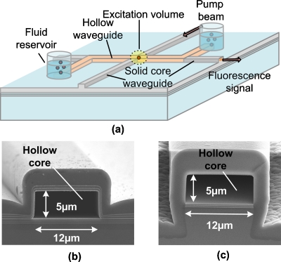
Hollow core ARROWs have been demonstrated using either wafer bonding or sacrificial etching approaches. For the former, hollow core channels were fabricated by first dry etching deep trenches into a silicon wafer.8, 9 Dielectric layers, serving as claddings, were deposited on the etched wafer as well as a flat wafer and the two were then bonded. For a fully self-contained sensing platform as shown in Fig. 1a, sacrificial etching techniques are preferable because this method provides great flexibility for integration of hollow core ARROWs with solid core waveguides, fluid reservoirs, and electrical elements. A fabrication process combining thin-film deposition and sacrificial etching also provides a good way to create ARROWs small enough for efficient fluorescence and Raman spectroscopy,10 down to single particles.11
Figure 1.
(a) ARROW based sensing platform. (b) SEM pictures of a hollow core waveguide fabricated with Ta2O5∕SiO2. (c) SEM picture of a hollow core waveguide fabricated with Ta2O5∕SiO2 on a self-aligned pedestal.
In order to build an optical sensing platform with high sensitivity, the signal-to-noise ratio (SNR) must be as high as possible. A significant source of noise when measuring fluorescence comes from the cladding materials of the waveguides. They can produce photoluminescence (PL) in the same wavelength range as the fluorescence or Raman signal generated by an analyte of interest located inside the waveguide. Because the background caused by the native PL of materials cannot be filtered out, subsequent SNR decreases.
Silicon dioxide (SiO2) and silicon nitride (SiN) have been used to fabricate ARROWs in previous structures.1, 2 However, silicon nitride has relatively high native PL at wavelengths of interest for fluorescence sensing. In this Letter, tantalum oxide (Ta2O5) is introduced as a replacement for SiN as a cladding material. Ta2O5 films are desirable because they have a refractive index (∼2.30 for sputtered film) comparable with SiN, high melting temperatures, low absorption in the visible wavelength, good adhesion to SiO2, and high resistance to acids.12 The design, fabrication, and optical measurements of a Ta2O5 and SiO2 ARROW are presented in this letter, with the goal of producing a waveguide with lower PL while maintaining low optical loss.
The fabrication process for hollow core Ta2O5∕SiO2 ARROWs is similar to the fabrication process used for SiN∕SiO2 ARROWs.2 To begin with, alternating SiO2 and Ta2O5 layers are coated by plasma-enhanced chemical vapor deposition (PECVD) and sputtering respectively. Ta2O5 can also be deposited by PECVD,13 however, the process is more complicated than that used for silicon based films (i.e., SiN and SiO2). SU-8 is then applied as a sacrificial material that forms a rectangular hollow core over the bottom layers. Six alternating dielectric layers are then deposited over the core, including a thick top oxide layer which is grown over the other five top layers to ensure mechanical strength. Substrate temperatures for both sputtering and PECVD are kept around 250 °C to ensure films are dense enough to survive an acid etching process for the removal of the SU8 core, which consisted of a piranha etch solution of sulfuric acid and hydrogen peroxide.14 Figure 1b shows a scanning electron microscope picture of a completed hollow ARROW with Ta2O5∕SiO2 films with a core 12 μm wide and 5.0 μm high. Sputtered Ta2O5 and PECVD SiO2 can also be used to make a structure as shown in Fig. 1c by depositing only one thick SiO2 layer on the top of the SU8 core after etching into the silicon substrate to form a self aligned pedestal.15
To build an on-chip ARROW platform shown in Fig. 1a, solid core waveguides are created on the same substrate to propagate optical signals on and off the chip and into and out of the hollow waveguides. The structure consists of the layers employed to create hollow core ARROWs, including the thick SiO2 layer used to increase the structural strength of the hollow waveguides. Ridges are then formed by plasma etching this topmost SiO2 layer. Light is guided in this layer, confined by ARROW layers beneath and air on top and on the sides (the air-SiO2 interfaces provide total internal reflection).
The optical loss of Ta2O5∕SiO2 solid and liquid-core ARROWs was compared to SiN∕SiO2 ARROWs. Solid core waveguides for both types of ARROWs were 12 μm wide and formed by etching a ridge 2 μm deep into the topmost SiO2 cladding layer. The dielectric layers were (starting from the substrate—in nm): SiO2∕Ta2O5∕SiO2∕Ta2O5∕SiO2∕Ta2O5∕SiO2 (281∕93∕281∕93∕281∕93-5000). Using the cutback method, a loss coefficient of 0.9±0.1 cm−1 was measured for Ta2O5∕SiO2 ARROWs and 0.7±0.1 cm−1 for SiN∕SiO2 ARROWs. For liquid-core ARROWs, the loss coefficients were measured by the scattering loss imaging method16, 17 when the cores were filled with water. The core dimensions for both the Ta2O5∕SiO2 and SiN∕SiO2 hollow core waveguides were 12×5 μm2. The dielectric layers for hollow core ARROW platform were: SiO2∕Ta2O5∕SiO2∕Ta2O5∕SiO2∕Ta2O5 -core-Ta2O5∕SiO2∕Ta2O5∕SiO2∕Ta2O5∕SiO2 (281∕93∕281∕93∕281∕93-5000-158∕281∕158∕281∕158∕5000). The hollow core loss was 2.7±0.2 cm−1 for SiN∕SiO2 samples and 3.1±0.2 cm−1 for Ta2O5∕SiO2 samples. These measurements clearly show that both types of waveguides have comparable losses and replacing the SiN layer with Ta2O5 does not add significantly to optical loss.
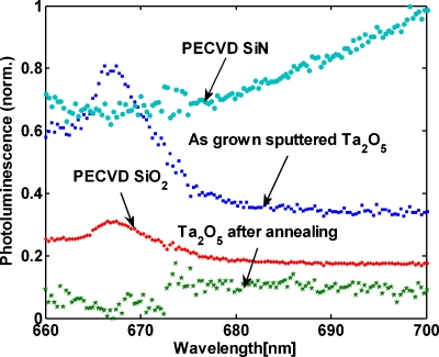
As mentioned above, it is preferable to use materials with low PL to fabricate waveguides in order to increase the sensitivity of fluorescence detection for ARROW platforms. Typically, the relevant PL range for cladding materials is from 660 to 690 nm for bimolecular detection on ARROWs with a pump beam of 633 nm. PL at other wavelengths can be removed with a band pass filter. To compare the PL from SiN based ARROWs with that from Ta2O5 based ARROWs, test films of 150 nm thickness were grown by sputtering and PECVD and measured by a spectrometer (Jobin, Yvon: LabRAM HR, λex=633 nm, P∼5 mW, 5 s integration time). Since alternating PECVD and sputtered films are coated in the ARROW fabrication process, the PL of the sputtered Ta2O5 film was measured before and after being annealed in the PECVD vacuum chamber at 250 °C. Figure 2 shows that an as-grown SiN PECVD film has higher PL than a PECVD SiO2 film or a Ta2O5 sputtered film. In particular, the PL intensity of Ta2O5 film drops substantially after annealing at 250 °C. This is fortunate for our end goal of producing a low PL waveguide since dense SiO2 PECVD films must be grown over the Ta2O5 films at 250 °C. It has been suggested that the annealing in an oxygen-free environment helps to reduce the density of midgap trap states in Ta2O5 films which are responsible for the PL.18
Figure 2.
PL of PECVD SiN and SiO2 films (T=250 °C) and sputtered Ta2O5 (T=250 °C), including as deposited films and after annealing in a vacuum chamber at 250° (excitation wavelength 633 nm).
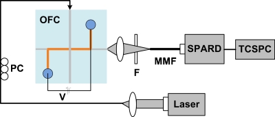
In order to explore and compare the detection sensitivity between SiN∕SiO2 ARROW chips and Ta2O5∕SiO2 ARROW chips, a previously described detection setup was employed11 (Fig. 3). A 633 nm pump light of 3.3 mW emitted from a HeNe laser was coupled into the solid-core waveguides on an ARROW platform [Fig. 1a]. The fluorescence signals generated at the excitation volume were collected via an objective lens (Olympus, NA=0.85). Spurious excitation photons were removed by collecting the fluorescence perpendicularly to the excitation direction and by optical filters (Semrock, 640 nm long pass and 670±17 nm bandpass) before coupling into an avalanche photodiode detector (APD, Perkin Elmer, SPCM-AQR-14-FC). The data were finally analyzed by using a time-correlated single photon counting card and software (Picoquant, Timeharp 200).
Figure 3.
Optical fluorescence setup. OFC: optofluidic chip; F: filter; PC: polarization controller; MMF: multimode fiber; SPAPD: single-photon avalanche photodiode; TCSPC: time-correlated single-photon counting card; V: applied voltage between fluid reservoirs.
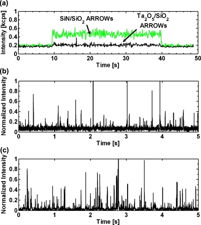
The PL intensity as a function of time from water filled (18MΩ-cm) SiN∕SiO2 and Ta2O5∕SiO2 ARROW chips are measured and compared in Fig. 4a. The liquid core channels were filled with water and the detector signal was recorded with laser off (t<10 s) and laser on (10 s<t<40 s). The experimental results show that the background noise baseline above the detector dark counts of liquid core ARROWs is reduced by a factor of 10 when SiN films are replaced by Ta2O5 films. Note that the total optical throughput from chip edge to edge (through both hollow and solid core waveguides) was approximately 10% for both types of ARROW chips.
Figure 4.
(a) Comparison of fluorescence background signals between SiN∕SiO2 samples and Ta2O5∕SiO2 samples. (b) Fluorescence signals from excited Tetraspeck nanoparticles in the excitation volume on SiN∕SiO2 ARROWs. (c) Fluorescence signals from excited Tetraspeck nanoparcles in the excitation volume on Ta2O5∕SiO2 ARROWs.
To characterize the SNR (detected signal divided by the standard deviation of the noise) of the devices, fluorescent nanoparticles (100 nm diameter, Tetraspeck, Invitrogen) were introduced into the chip via the reservoir [Fig. 1a, 10 μl]. The particle concentration (1.8×10¹⁰ particles∕ml) was chosen such that only one particle was detected in the device excitation volume (∼85 fl using 1∕e2 beam diameters). The particles traveled down the channel using pressure driven flow and were optically excited at the orthogonal hollow core∕solid core interface. The particle fluorescence was then collected by the APD. The detected signals for SiN∕SiO2 and Ta2O5∕SiO2 devices are shown on Figs. 4b, 4c (over a 5 s span), respectively, where each spike corresponded to a detected nanoparticle. The device baseline and noise was clearly higher in Fig. 4b than in Fig. 4c. Over a 40 s timeframe, the number of detected particles for the Ta2O5∕SiO2 sample was 948, with an average SNR of 126.7. The number of detected particles for the SiN∕SiO2 ARROW sample was 53, with an average SNR of 10.3. In other words, the number of detected particles increased by a factor of 18 and the SNR improved by a factor of 12 by replacing SiN with Ta2O5 films.
In conclusion, Ta2O5 films were investigated as a replacement for SiN films for the construction of hollow core and solid core ARROWs. Ta2O5 based ARROWs were shown to have comparable optical losses to their SiN counterparts. Fluorescence measurements also show that the background noise between 660 and 690 nm has been reduced by a factor of 10 by replacing SiN with Ta2O5 films. The SNR of Ta2O5∕SiO2 ARROWs was around 12 times higher than that of SiN∕SiO2 ARROWs. This improved material system allows for more sensitive measurements, including pushing detection limits down to the level of single fluorophores.
Acknowledgments
This work was supported by the NIH∕NIBIB (R01EB006097), NSF (ECS-0528730, ECS-0528714), and the W. M. Keck Center for Nanoscale Optofluidics at the University of California at Santa Cruz.
References
- Schmidt H. and Hawkins A. R., Microfluid. Nanofluid. 4, 3 (2008). 10.1007/s10404-007-0199-7 [DOI] [PMC free article] [PubMed] [Google Scholar]
- Hawkins A. R. and Schmidt H., Microfluid. Nanofluid. 4, 17 (2008). 10.1007/s10404-007-0194-z [DOI] [PMC free article] [PubMed] [Google Scholar]
- Yeh P. and Yariv A., Opt. Commun. 19, 427 (1976). 10.1016/0030-4018(76)90115-2 [DOI] [Google Scholar]
- Russell P., Science 299, 358 (2003). 10.1126/science.1079280 [DOI] [PubMed] [Google Scholar]
- Lo S., Wang M., and Chen C., Opt. Express 12, 6589 (2004). 10.1364/OPEX.12.006589 [DOI] [PubMed] [Google Scholar]
- Cadarso V. J., Llobera A., Salinas I., Izquierdo D., Garcés I., and Domínguez C., Opt. Commun. 281, 1568 (2008). 10.1016/j.optcom.2007.11.028 [DOI] [Google Scholar]
- Yin D., Barber J. P., Hawkins A. R., Deamer D. W., and Schmidt H., Appl. Phys. Lett. 85, 3477 (2004). 10.1063/1.1807966 [DOI] [Google Scholar]
- Bernini R., Nuccio E. D., Minardo A., Zeni L., and Sarro P. M., IEEE J. Quantum Electron. 13, 194 (2007). 10.1109/JSTQE.2007.894054 [DOI] [Google Scholar]
- Testa G., Huang Y., Zeni L., Sarro P. M., and Bernini R., IEEE Photonics Technol. Lett. 22, 616 (2010). 10.1109/LPT.2010.2043352 [DOI] [Google Scholar]
- Yin D., Lunt E. J., Barman A., Hawkins A. R., and Schmidt H., Opt. Express 15, 7290 (2007). 10.1364/OE.15.007290 [DOI] [PubMed] [Google Scholar]
- Yin D., Lunt E. J., Rudenko M. I., Deamer D. W., Hawkins A. R., and Schmidt H., Lab Chip 7, 1171 (2007). 10.1039/b708861b [DOI] [PubMed] [Google Scholar]
- Inci M. N. and Yoshino T., Opt. Rev. 7, 205 (2000). 10.1007/s10043-000-0205-8 [DOI] [Google Scholar]
- Kim I., Chun J. S., and Lee W., Mater. Chem. Phys. 44, 288 (1996). 10.1016/0254-0584(96)80072-1 [DOI] [Google Scholar]
- Holmes M., Keeley J., Hurd K., Schmidt H., and Hawkins A. R., J. Micromech. Microeng. 20, 115008 (2010). 10.1088/0960-1317/20/11/115008 [DOI] [PMC free article] [PubMed] [Google Scholar]
- Lunt E. J., Wu B., Keeley J. M., Measor P., Schmidt H., and Hawkins A. R., IEEE Photonics Technol. Lett. 22, 1147 (2010). 10.1109/LPT.2010.2051145 [DOI] [PMC free article] [PubMed] [Google Scholar]
- Wang H., Appl. Opt. 33, 1707 (1994). 10.1364/AO.33.001707 [DOI] [PubMed] [Google Scholar]
- Strasser A. T. and Gupta M. C., Appl. Opt. 31, 2041 (1992). 10.1364/AO.31.002041 [DOI] [PubMed] [Google Scholar]
- Alers G. B., Fleming R. M., Wong Y. H., Dennis B., and Pinczuk A., Appl. Phys. Lett. 72, 1308 (1998). 10.1063/1.120569 [DOI] [Google Scholar]


