Abstract
Silicon nitride membranes can be used for windows of environmental chambers for in situ electron microscopy. We report that aberration corrected scanning transmission electron microscopy (STEM) achieved atomic resolution on gold nanoparticles placed on both sides of a 50-nm-thick silicon nitride membrane at 200 keV electron beam energy. Spatial frequencies of 1∕1.2 Å were visible for a beam semi-angle of 26.5 mrad. Imaging though a 100-nm-thick membrane was also tested. The achieved imaging contrast was evaluated using Monte Carlo simulations of the STEM imaging of a sample of with a representative geometry and composition.
The introduction of aberration correctors for scanning transmission electron microscopy (STEM) has made it possible to achieve subangstrom probe sizes.1, 2 Now that these ultimate resolution values have been achieved, the field of in situ electron microscopy of materials at gaseous and liquid environments is gaining prominence in material science and biological research.3, 4, 5, 6, 7In situ TEM with atomic resolution on specimens in gaseous environments has already been demonstrated for subambient pressures3, 4 using differentially pumped systems. Ambient pressures and higher were achieved by the use of environmental chambers fully enclosed by thin windows of silicon nitride (SiN).6, 8 To achieve high pressures the window should be as small and thick as possible while for high-resolution electron microscopy the windows should be as thin as possible, i.e., to avoid beam blurring in the window. So far, atomic resolution was demonstrated for SiN window thicknesses of ∼10 nm.6, 9 However, for the design of in situ systems it is important to be able to use SiN windows of 30 nm and thicker,10 since these can be manufactured in commercial processes without holes, and allow much larger window sizes in combination with high pressures than the ultrathin windows,11 with advantages also for the alignment of two windows forming an environmental chamber.12 An important question is thus if atomic resolution imaging can still be achieved for SiN membranes thicker than 30 nm. In this letter, we show aberration corrected STEM imaging of gold nanoparticles with atomic resolution through SiN membranes of 50, a standard thickness for membranes spanning hundreds of micrometers.
The samples were prepared by depositing gold nanoparticles on both sides of 50-nm-thick SiN membranes on silicon microchips (SPI); windows of 100 nm thickness were also tested. Gold nanoparticles (Ted Pella) of sizes 2, 5, 10, and 30 nm in saline water solution were mixed together and diluted with ethanol. A second water∕ethanol solution containing gold nanoparticles of a size of 1.4 nm (Nanoprobes) was also prepared. Each solution was mixed for about 2 min in an ultrasonic bath. The nanoparticle solutions were then applied from ∼0.2 μl droplets to both sides of the SiN membranes and dried in air (∼3 min). The silicon microchips were then cleaned with ethanol. Finally the microchips were plasma cleaned for ∼30 s on each side to avoid contamination during STEM imaging. Plasma cleaning possibly led to the breaking of a few nanoparticles into fragments, and in some cases, individual gold atoms.
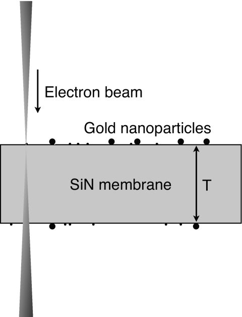
The samples were imaged with a 200 kV aberration corrected STEM∕TEM (JEOL, 2200 FS) adjusted at an electron beam opening semiangle of α=26.5 mrad and a probe current of 30 pA. The geometry of the experiment is shown in Fig. 1. The corrector was aligned on the same day of and prior to the imaging. The SiN membranes were preirradiated with a dose of ∼8×10⁴ e−∕nm2. This procedure called “beam shower” was performed by scanning the sample at the eucentric height with a defocused beam at a magnification of 50,000×, with the purpose to avoid contamination during subsequent imaging at high magnification;13 this procedure does not damage the specimen. It was also observed that gold nanoparticles of samples that were subjected to a beam shower showed stronger adherence to the support membranes, i.e., did not move during imaging. The high angle annular dark field (HAADF) detector was used to collect the signals. All images were recorded at a magnification of 10,000,000 (pixel size of 0.028 nm), an image size of 512×512 pixels, and a pixel dwell time of 32 μs. The actual thickness of the SiN membrane was measured by determining the vertical positions at which the gold particles were at focus at the top and at the bottom of the membrane, respectively, in a three-dimensional focal series. This measurement was repeated for ten different positions on SiN membrane, yielding a thickness of 45.7±3.9 nm (the error being the standard deviation).
Figure 1.
Schematic representation of STEM of gold nanoparticles on the top and at the bottom of a SiN membrane of thickness T. The electron beam direction is downward.
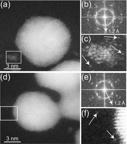
Figure 2a shows the STEM HAADF image of gold nanoparticles on top of a SiN membrane, with respect to the beam direction from the top to bottom. Figure 2d shows an image of gold nanoparticles at the bottom of the SiN membrane. The lattice fringes of the gold nanoparticles are visible in both images. The fast Fourier transforms (FFTs) of these images show intensity spots out to spatial frequencies of 1∕1.2 Å [Figs. 2b, 2e]. This spatial frequency is consistent with the theoretical resolution limit of the aberration corrected STEM, which was calculated from the diameter d59 that contains 59% of the probe current incident on the specimen. The value of d59=1 Å, for α=26.5 mrad, for a 200 keV electron probe corrected for spherical aberrations up to third order, and with Cc=0.75 mm, dE=2 eV, and C5=5 mm.14 Figures 2c, 2f show enlarged sections of their respective original images showing single gold atoms for both sides of the SiN membrane. Hence, for a SiN membrane of 50 nm thickness, atomic resolution was achieved irrespective of whether the gold nanoparticles were on the top or bottom of the membrane. Imaging at α=17.3 mrad and 41 mrad (data not shown) showed a similar spatial resolution.
Figure 2.
Aberration corrected STEM of gold nanoparticles on a 50-nm-thick SiN membrane. (a) Image of gold nanoparticles on the top of the SiN membrane. (b) FFT of the image in (a). (c) Magnified image of the area selected by the rectangle in (a) showing single atoms; examples are indicated by the arrows. (d) Image of gold nanoparticles at the bottom of the SiN membrane. (e) FFT of image (d). (f) Selection (rectangle) from (d).
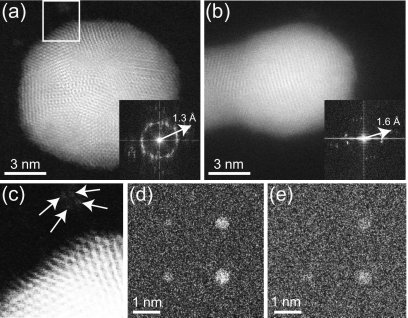
For comparison we have also imaged gold nanoparticles on a 100-nm-thick SiN membrane. Figure 3a shows gold nanoparticles on top of the SiN membrane, lattice fringes are clearly visible in the image. The FFT of Fig. 3a exhibited intensity spots out to a spatial frequency of 1∕1.3 Å. Single gold atoms can still be discerned in the left upper corner of the image and are shown magnified in Fig. 3c. The STEM image of a gold nanoparticle on the bottom of a 100-nm-thick SiN membrane is shown in Fig. 3b. The corresponding FFT includes spatial frequencies up to 1∕1.6 Å. Figure 3b shows lattice fringes in at least three different directions while five different orientations are visible in the FFT. The resolution obtained on gold nanoparticles at the bottom of the 100-nm-thick SiN was also verified for two other nanoparticles. The FFTs of these images included spatial frequencies of maximal 1∕2.0 Å with different directions than for Fig. 3b, thus ruling out a preferential nanoparticle∕fringe orientation. To ensure that this reduction in resolution was not due to incorrect stigmation, a focal series was recorded. The focal series showed particles going in and out of focus in a spherical shape rather than cigar shape, thus confirming correct stigmator settings. Therefore, the average resolution was 1.9 Å for STEM imaging at the bottom of a 100-nm-thick SiN membrane, a reduction of 0.6 Å with respect to imaging at the top of the window.
Figure 3.
The effect of beam broadening. (a) STEM image of gold nanoparticles on top of a 100-nm-thick SiN membrane. The FFT is shown in the inset. (b) Image recorded at the bottom of the SiN membrane in (a), with the FFT shown in the inset. (c) Magnified image of the area selected by the rectangle in (a) showing four single atoms indicated by the arrows. (d) Monte Carlo simulations of gold nanoparticles with diameters of 0.3, 0.4, 0.5, and 0.6 nm placed in a 2×2 matrix at the bottom of a SiN membrane of 50 nm. (e) Same as in (d), but then for a membrane thickness of 100 nm.
The observation of a reduced resolution for imaging at the bottom of a 100-nm-thick SiN membrane compared to imaging at the top can be explained by electron beam scattering. Nanoparticles at the top were imaged with an unperturbed electron probe while nanoparticles at the bottom were imaged with an electron probe that had already interacted with the membrane, causing a skirt of scattered electrons around the unscattered electron probe. Scattering led to a decrease in the contrast, and in addition, a broadening of the focused electron probe. The broadening due to elastic scattering though a material of thickness T can be expressed as width of an intensity distribution across a sharp edge, where the intensity goes from 25% to 75% of the total intensity, x25–75,15
| (1) |
| (2) |
with electron accelerating voltage U (in volt), atomic number Z, the rest mass of the electron, the speed of light c, and the electron charge e. The chemical composition of the SiN window approximately equals that of Si3N4, with ρ=3.2×10⁶ g∕m3, W=3∕7×28+4∕7×14=20.0 g∕mol, and Z=√(3∕7×142+4∕7×72)=10.6. The calculation gives x25–75=3 Å and 8 Å, for T=50 nm and 100 nm, respectively. Previous experimental data recorded under conditions not compatible with atomic resolution using a noncorrected STEM showed a resolution of 0.4 nm on gold nanoparticles below a 50-nm-thick SiN membrane.8 The calculated numbers and previous data seem too pessimistic considering the present experimental data.
To provide a more realistic calculation of the beam blurring we have simulated the imaging of gold nanoparticles at the bottom of a SiN membrane with Monte Carlo methods in a modified version of the software CASINO with electron scattering models for the energy range of the STEM implemented.16 Figures 3d, 3e show simulated STEM images of gold nanoparticles of different sizes for SiN thickness of 50 and 100 nm, simulated with the same parameters as used in the experiment. For the 50 nm membrane the nanoparticle with a diameter of 0.3 nm (which is the smallest atomic diameter of the gold particle in the SiN membrane) is still visible in the noise at the left upper corner while it vanished in the noise for the thicker membrane. This result is consistent with the experimental findings.
Our results show that spatial frequencies of 1∕1.2 Å, and individual gold atoms are visible when imaging gold nanoparticles positioned on both sides of a 50-nm-thick SiN membrane, using an aberration corrected STEM at 200 keV. Dedicated environmental chambers may be designed for in situ STEM imaging of samples containing gold atoms, for example, to examine the behavior of gold catalysts,17 or the growth of nanomaterials at the solid–gas interface.18 Windows of 30 nm thickness and with dimensions as large as 0.1 mm withstand a pressure difference over 1 atm.10 Membrane devices can be combined with technology for rapid heating.7
Acknowledgments
We thank D. Drouin, D. C. Joy, and L. F. Allard for discussions and help with the experiments. Electron microscopy conducted at the Shared Research Equipment user facility at Oak Ridge National Laboratory sponsored by the Division of Scientific User Facilities, U.S. Department of Energy. Research supported by NIH Grant No. R01GM081801.
References
- Krivanek O. L., Nellist P. D., Dellby N., Murfitt M. F., and Szilagyi Z., Ultramicroscopy 96, 229 (2003). 10.1016/S0304-3991(03)00090-1 [DOI] [PubMed] [Google Scholar]
- Nellist P. D., Chisholm M. F., Dellby N., Krivanek O. L., Murfitt M. F., Szilagyi Z. S., Lupini A. R., Borisevich A., W. H.Sides, Jr., and Pennycook S. J., Science 305, 1741 (2004). 10.1126/science.1100965 [DOI] [PubMed] [Google Scholar]
- Boyes E. D. and Gai P. L., Ultramicroscopy 67, 219 (1997). 10.1016/S0304-3991(96)00099-X [DOI] [Google Scholar]
- Helveg S., Lopez-Cartes C., Sehested J., Hansen P. L., Clausen B. S., Rostrup-Nielsen J. R., Abild-Pedersen F., and Norskov J. K., Nature (London) 427, 426 (2004). 10.1038/nature02278 [DOI] [PubMed] [Google Scholar]
- de Jonge N., Peckys D. B., Kremers G. J., and Piston D. W., Proc. Natl. Acad. Sci. U.S.A. 106, 2159 (2009). 10.1073/pnas.0809567106 [DOI] [PMC free article] [PubMed] [Google Scholar]
- Creemer J. F., Helveg S., Hoveling G. H., Ullmann S., Molenbroek A. M., Sarro P. M., and Zandbergen H. W., Ultramicroscopy 108, 993 (2008). 10.1016/j.ultramic.2008.04.014 [DOI] [PubMed] [Google Scholar]
- Allard L. F., Bigelow W. C., Jose-Yacaman M., Nackashi D. P., Damiano J., and Mick S. E., Microsc. Res. Tech. 72, 208 (2009). 10.1002/jemt.20673 [DOI] [PubMed] [Google Scholar]
- de Jonge N., Bigelow W. C., and Veith G. M., Nano Lett. 10, 1028 (2010). 10.1021/nl904254g [DOI] [PubMed] [Google Scholar]
- Creemer J. F., Helveg S., Hoveling G. H., Ullmann S., Molenbroek A. M., Sarro P. M., and Zandbergen H. W., J. Microelectromech. Syst. 19, 254 (2010). 10.1109/JMEMS.2010.2041190 [DOI] [Google Scholar]
- Nishiyama H., Suga M., Ogura T., Maruyama Y., Koizumi M., Mio K., Kitamura S., and Sato C., J. Struct. Biol. 169, 438 (2010). 10.1016/j.jsb.2010.01.005 [DOI] [PubMed] [Google Scholar]
- Ciarlo D. R., Biomed. Microdevices 4, 63 (2002). 10.1023/A:1014275913962 [DOI] [Google Scholar]
- Ring E. A. and de Jonge N., Microsc. Microanal. 16, 622 (2010). 10.1017/S1431927610093669 [DOI] [PubMed] [Google Scholar]
- Egerton R. F., Li P., and Malac M., Micron 35, 399 (2004). 10.1016/j.micron.2004.02.003 [DOI] [PubMed] [Google Scholar]
- Haider M., Uhlemann S., and Zach J., Ultramicroscopy 81, 163 (2000). 10.1016/S0304-3991(99)00194-1 [DOI] [PubMed] [Google Scholar]
- Reimer L., Transmission Electron Microscopy (Springer, Heidelberg, 1984). [Google Scholar]
- Demers H., Poirier-Demers N., Drouin D., and de Jonge N., Microsc. Microanal. 16, 795 (2010). 10.1017/S1431927610094080 [DOI] [PMC free article] [PubMed] [Google Scholar]
- Veith G. M., Lupini A. R., and Dudney N. J., J. Phys. Chem. C 113, 269 (2009). 10.1021/jp808249f [DOI] [Google Scholar]
- Hofmann S., Sharma R., Wirth C. T., Cervantes-Sodi F., Ducati C., Kasama T., Dunin-Borkowski R. E., Drucker J., Bennett P., and Robertson J., Nature Mater. 7, 372 (2008). 10.1038/nmat2140 [DOI] [PubMed] [Google Scholar]


