Abstract
We report the experimental observation of a trapped rainbow in adiabatically graded metallic gratings, designed to validate theoretical predictions for this unique plasmonic structure. One-dimensional graded nanogratings were fabricated and their surface dispersion properties tailored by varying the grating groove depth, whose dimensions were confirmed by atomic force microscopy. Tunable plasmonic bandgaps were observed experimentally, and direct optical measurements on graded grating structures show that light of different wavelengths in the 500–700-nm region is “trapped” at different positions along the grating, consistent with computer simulations, thus verifying the “rainbow” trapping effect.
Keywords: slow light, surface dispersion engineering, surface plasmons
Since Ebbesen et al.’s report on extraordinary optical transmission through plasmonic hole arrays was published in 1998 (1), the study of plasmonics and metamaterials (2) has progressed at a rapid pace and led to the discovery of phenomena with unique optical properties. For example, recent theoretical investigations reported the “trapped rainbow” storage of terahertz waves in metamaterials (3) and plasmonic graded structures (4), and generated considerable interest for slow-light applications. It was predicted that tapered waveguides with a negative refractive index core (3) and graded metallic grating structures (4, 5) were capable of slowing a broadband rainbow to a standstill. By varying the nanotopology of metal surfaces, the optical properties of surface plasmon polaritons (SPPs) can be tailored via so-called surface dispersion engineering (6–8). Moreover, by scaling the feature size of the graded grating structures down to the nanometer scale, it was theoretically predicted that telecommunication waves and even visible waves can also be trapped (9, 10).
The intrinsic slow-light properties of SPP modes in 1D metallic grating structures can be seen from their dispersion relations, where their group velocity vg is found to decrease significantly as the photonic band edge is approached. Our recent investigations of simple 1D metallic gratings demonstrated that the surface dispersion properties can be tuned by systematically varying the groove depth and grating period. The dispersion relations for adiabatically graded gratings vary monotonically with position, so that incoming waves at different wavelengths can be trapped or localized at different positions along the propagation direction of the grating.
Advances in nanofabrication and characterization techniques now permit the experimental demonstration of this interesting class of structures. Rainbow trapping has not yet been unambiguously demonstrated in the visible regime for either metamaterials (3) or plasmonic structures (4, 5, 9), although in related studies photonic crystal nanocavities with graded hole size were recently shown to exhibit adiabatically reduced group velocities for photonic modes at telecommunication frequencies (11). Two preliminary efforts were recently reported to realize the trapped rainbow in tapered metamaterial waveguides (12, 13). However, there is currently no clear pathway for realizing negative refractive indices materials over a broad range of visible wavelengths (2, 14), as required for the tapered metamaterial waveguide concept (3). On the other hand, the adiabatically graded plasmonic gratings are convenient and practical structures that can be readily realized by modern nanofabrication techniques. In the present work, one-dimensional adiabatically graded metallic grating structures were designed, fabricated, and experimentally characterized.
The first part of this paper describes the tailoring of the surface dispersion properties by tuning the nanopatterned groove depth and grating period. Experimental interferometric measurements are performed to confirm key features of the theoretically predicted SPP dispersion properties, including observation of the photonic bandgap, and variation of the cutoff wavelength with groove depth. Finally, rainbow trapping in graded grating structures is experimentally demonstrated at room temperature in the visible domain. Due to the large decrease in the SPP group velocity at a specific position along the adiabatic grating surface, the SPP modes are predicted to accumulate at this position (4, 9). Scattering from SPP modes propagating along the nanopatterned surface permits probing of the localized intensity of the surface-confined SPP mode as a function of position by far-field optical microscopy. These measurements confirm that SPP modes of different wavelengths are localized at different positions along the graded grating, thus validating the theoretical predictions of “rainbow trapping.” Such solid-state plasmonic slow-light structures provide a means to control the group velocity (15), with the potential for incorporation into light-based (photonic) logic circuits.
Surface Dispersion Engineering of 1D Metallic Groove Arrays
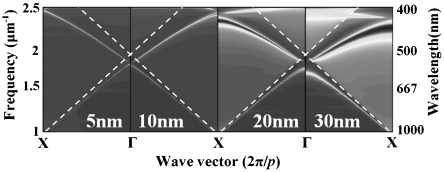
To illustrate the tunability of the dispersion curves of nanopatterned surfaces, angular-dependent reflection spectra of silver grating surfaces were calculated using the rigorous coupled-wave analysis (RCWA) method,* and their corresponding dispersion curves are plotted in Fig. 1 for a series of groove depths. The grating period and groove width are 520 and 150 nm, respectively. The calculated dispersion relations in the first Brillouin zone exhibit a downward curvature relative to the free-space light lines, indicating a reduced vg for the SPP modes. Note that the vg reduction is greater for larger groove depths. Fig. 1 also shows the surface photonic bandgap for these periodic nanopatterns (6–8), which is located roughly in the 540–560 nm wavelength region and broadens with increasing groove depth. SPP modes in this frequency region cannot be supported by this nanopatterned surface. Such groove structures have been suggested as a surface distributed Bragg reflector for a unidirectional surface wave coupler (16) or a bidirectional plasmonic splitter (17, 18). Similar modeling also demonstrates how the shape of the dispersion curves can be tailored by varying the grating period (SI Text and Fig. S1).
Fig. 1.
Dispersion curves of the nanopatterned silver gratings with groove depths of 5, 10, 20, and 30 nm, calculated by the RCWA method. The dashed lines are light lines in free space. In these calculations, the period and width of the grooves are 520 and 150 nm, respectively.
Experimental Verification of Surface Dispersion Engineering
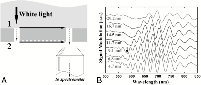
To confirm the above theoretical predictions of surface dispersion engineering experimentally, a series of 1D nanopatterned gratings with different groove depths were fabricated using focus ion beam (FIB) milling (FEI Dual-Beam System 235). Eight gratings were fabricated on a 300-nm-thick layer of Ag that had been evaporated onto flat fused silica microscope slides (Fisherbrand). The period and the width of this series of gratings were approximately 520 and 150 nm, respectively. The eight structures have groove depths of 4.7( ± 0.2), 6.8( ± 0.1), 9.1( ± 0.2), 11.7( ± 0.5), 14.5( ± 0.5), 16.7( ± 0.5), 20.2( ± 0.7), and 23.9( ± 0.9) nm as measured by an atomic force microscope (AFM; Asylum Research MFP-3D) with an ultrasharp tip (NanoAndMore USA, Inc., SSS-NCH AFM probes). SEM images of two gratings with groove depths of approximately 4.7 and 23.9 nm are shown in Fig. 2. Next, two nanoslits were patterned on opposite sides of each grating structure to function as the input and output couplers (19) for a plasmonic Mach–Zehnder interferometer (MZI) (20), as illustrated in Fig. 3A. The slit separation distance for these samples is approximate 21 μm. Both the top metal–glass interface 1 and bottom metal–air interface 2 can support SPP modes. When SPP modes excited by the slit on the left propagate to the right slit, the SPP signals from the upper and lower optical branches interfere with each other and modulate the far-field distribution of the scattered waves. This plasmonic MZI permits experimental characterization of the optical properties of the surface grating structures and validation of the predicted bandgaps as a function of groove depth.
Fig. 2.
SEM images of two gratings with groove depths of 4.7 and 23.9 nm. The period and the width of this series of gratings were approximately 520 and 150 nm, respectively.
Fig. 3.
(A) Illustration of apparatus for plasmonic MZI interoferometric measurements. (B) SPP-mediated spectral interference introduced by the SPP modes from the top and bottom surfaces: Here we study eight doublet samples on an Ag film with groove depths of 4.7( ± 0.2), 6.8( ± 0.1), 9.1( ± 0.2), 11.7( ± 0.5), 14.5( ± 0.5), 16.7( ± 0.5), 20.2( ± 0.7), and 23.9 nm( ± 0.9).
Measurement of the modulated far-field transmission of the plasmonic MZI as a function of wavelength permits detection of the SPP bandgap of the grating structure at the metal–air interface. Variations in the bandgap of SPP modes for different nanopatterend surfaces are detected from changes in their interference patterns. The onset of reductions in vg is also determined. The far-field interference pattern varies as (19) (see SI Text)
 |
[1] |
where neff is the effective refractive index of the metal–dielectric interface, L is the slit separation distance, and φ0 is an additional phase shift. For the flat interface 1, the effective refractive index is given by the expression
 |
where  is the real part of the metal permittivity, and n1 is the refractive index of the substrate. For the nanopatterned interface 2, neff2 changes with grating geometry.
The measured interference oscillations for the eight plasmonic MZIs are shown in Fig. 3B. In this data, the low-frequency background and high-frequency noise have been numerically filtered using a fast Fourier transform technique (with a low-frequency cutoff of approximately 4.344 μm-1 and high-frequency cutoff of approximately 101.358 μm-1). The observed interference oscillations in the 570–580-nm wavelength region decrease in amplitude and eventually disappear with increasing groove depth (as shown by the black arrow), indicating the presence of an SPP bandgap. The data show that the bandgap broadens as the groove depth increases, consistent with theoretical predictions (19) (see Fig. S2). For grooves deeper than 10 nm, interference oscillations are not observed on the short wavelength side of the bandgap, because of the increased loss of SPP modes that are more tightly confined at these higher frequencies. To further confirm the tunability of the SPP bandgap, a series of four structures was also fabricated with grating period and groove width of approximately 635 and 200 nm, respectively. For these structures, the interference oscillations disappear between the wavelengths of 660 and 700 nm as the groove depth increases, indicating a shift of the bandgap to longer wavelengths (19) (see Fig. S3). These measurements provide clear evidence that the surface dispersion properties can be tuned by tailoring the dimensions of the nanopatterned surface.
It is also possible to determine the group velocity vg2 and group index ngr = c/vg2 of the SPP modes at the nanopatterned air–Ag interface, by measuring the peak and valley wavelengths of interference oscillations. The derived group index at the metal–air interface increases up to 1.35 for nanopatterned surfaces in the spectral region of 600–800 nm, as shown in Fig. S4 (19). Although this increase is modest, the data show that it occurs over a broad range of wavelengths and that the group index increases with increasing groove depth, as predicted. These experimental data demonstrate the broadband slowing of light in nanoengineered plasmonic structures. In principle, it should be possible to determine significantly larger group indices, but that is difficult using the current sample geometry (see Fig. S5). Although the group index increases as the groove depth increases, neff becomes closer for the two arms of the plasmonic MZI, increasing the period of the interference pattern and making observation near the band edge more difficult (19) (see SI Text). Nevertheless, from the theoretical simulation results in Fig. 1, one can estimate that the vg2 decreases to 0.01c at the band edge (here c is the light speed in the free space).
Metallic Graded Gratings
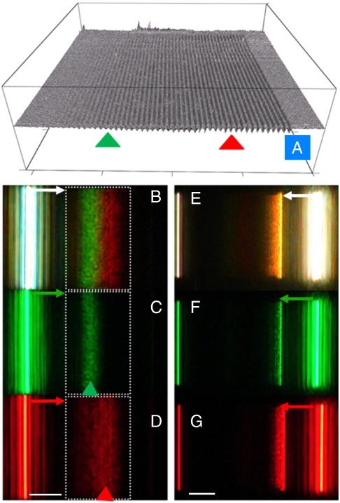
We now discuss the fabrication and experimental characterization of graded grating structures to verify the trapped rainbow effect, which is the primary focus of this paper. Employing the principles of surface dispersion engineering discussed above, a graded grating was designed for the 500–700-nm wavelength region, and fabricated by FIB milling, with a grating period and groove width of approximately 475 and 150 nm, respectively (see Fig. 4A). The surface topology was measured by AFM. The milling time for each successive groove was incrementally increased to achieve a grating with a linearly graded groove depth. AFM measurements results (see Fig. 4A) indicate that the surface roughness at the bottom of the grooves is approximately 0.3 nm, and the groove depth increases by approximately 1.8 nm with each step. A nanoslit was fabricated 13 μm from the left edge of the graded grating to couple free-space light incident from the bottom to SPP modes on the top surface (indicated by arrows in Fig. 5 B–G). Light emanating from the nanogrooves is observed from the top side. White light illumination was passed through a multiband filter (Semrock, with transmission bands centered at 542 and 639 nm), and a colorful emission at red and green wavelengths is observed at different positions on the grating and shown in Fig. 4B, demonstrating the rainbow trapping effect. Subsequently, two bright line filters (Semrock) at 546 (bandwidth 6 nm) and 655 nm (bandwidth 12 nm) were used to narrow the range of illumination wavelengths. Our theoretical simulations indicate that the green light at 546 nm and red light at 655 nm should be trapped at groove depths of approximately 30 and 70 nm, respectively (as indicated by the triangles in Fig. 4A). The experimental results in Fig. 4 C and D show that the green and red SPP emissions extend to different positions along the graded grating structure, and their central positions agree reasonably well with the theoretical predictions. The bright regions in these figures are relatively broad, arising in part from increased scattering loss caused by surface roughness at the bottom of the nanogrooves and the breadth of the dispersion curve at the photonic band edge and resulting spread in vg and propagation loss.
Fig. 4.
(A) The AFM image of a graded grating. The period and the width of the grooves are approximately 475 and 150 nm, respectively. The groove depth increases from approximately 6 to 100 nm. B–D are images of the emission from the structure with different filters, respectively. E–G are emission images with the SPP modes coupled and propagating in a direction opposite to that for B–D. (Scale bar: 10 μm.)
Fig. 5.
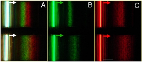
Microscope images of graded gratings with different gradients. In this measurement, three filters are employed: (A) a multiband filter (Semrock, transmission bands centered at 542 and 639 nm), (B) a green filter centered at 546 nm (bandwidth 6 nm), and (C) a red filter centered at 655 nm (bandwidth 12 nm). (Scale bar: 10 μm.)
If the SPP modes were excited and guided from the opposite side of the grating, they would reach the deepest groove first, which is approximately 100 nm in depth. Theory predicts that the SPP modes should be scattered at once without propagating into the waveguide. To confirm this prediction experimentally, we fabricated another nanoslit positioned 13 μm from the right edge of the graded grating. This nanoslit couples the incident light to SPP modes and guides them toward the grating in the opposite direction. It is obvious from Fig. 4 E–G that the emission is scattered at the deepest grooves without further propagation into the surface grating waveguide, as can be seen by comparison with the images shown in Fig. 4 B–D.
According to our previous simulations (4), varying the grade of the groove depths permits tuning of the locations at which light of different wavelengths are trapped. To validate this prediction, we fabricated another graded grating structure, whose period and width are fixed at 475 and 150 nm, respectively. The milling time for each groove was decreased by a factor of two, and the number of the grooves was doubled. AFM measurements indicate that the groove depth increased approximately 1.0 nm for each incremental step. The nanoslit input coupler was again fabricated 13 μm from the left edge of the graded grating. Fig. 5 shows the microscope images of the two graded grating structures side by side for comparison. The propagation direction of the SPPs launched by the nanoslit is indicated by the arrows. As predicted, the center positions of the trapped green and red emissions are shifted slightly to the right, and the SPP emission bands are slightly broader for the more slowly graded structure. These results validate the predictions of the numerical simulations (9) and demonstrate the tuning of the local dispersion properties of the graded plasmonic gratings.
We now consider the extent to which the grating structures employed in our experiments may be considered adiabatically graded. The criterion for validity of the adiabatic or Wentzel–Kramers–Brillouin approximation is (21–23)
| [2] |
The groove depth of the graded nanogratings increases by a fixed step size from one period to the next. Consequently, Eq. 2 may be rewritten
 |
[3] |
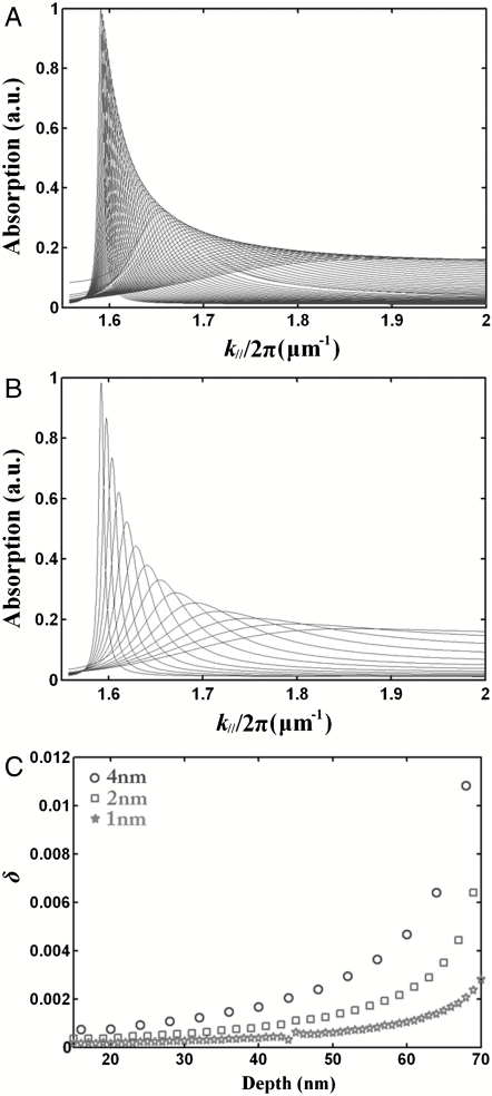
where P is the period of the grating. Angular-dependent absorption spectra were calculated by RCWA techniques for a series of metallic gratings with different groove depths. In this modeling, A = 1 - R, where A is the absorption and R is the reflection. The results are shown in Fig. 6 A and B, assuming a free-space wavelength of 655 nm. From sample to sample, the groove depth is assumed to change from 15 to 70 nm in increments of 1 nm in Fig. 6A and from 16 to 68 nm in increments of 4 nm in Fig. 6B. The calculated results clearly show that the resonant peak shifts with the groove depth of the grating, and that the peak shift is larger for Fig. 6B than for Fig. 6A, because of the larger incremental change in groove depth. Eq. 3 is employed to estimate the adiabatic parameter, δ, directly from the numerical simulation results in Fig. 6 A and B. The resulting values of δ, plotted in Fig. 6C for three different grating pitches, are found to increase as the depth approaches the “trapping” position, corresponding to the Brillouin zone boundary for this wavelength. The uncertainty in determining δ increases close to the zone boundary, where the resonant spectrum is broader and the peak position more difficult to determine accurately. Fig. 6C shows that the adiabaticity condition δ ≪ 1 is still met as the grating depth changes from 16 to 68 nm in increments of 4 nm. Consequently, nanogratings with smaller depth changes, shown in Figs. 4 and 5, can be regarded as adiabatically graded nanostructures. Such feature sizes are realizable using current nanofabrication techniques.
Fig. 6.
Absorption resonant spectra for an incident wavelength of 655 nm. The depth changes by 1 nm from sample to sample in A and by 4 nm in B. The adiabatic parameter, δ, for three different incremental depth changes of 1, 2, and 4 nm are plotted as a function of groove depth in C.
Future investigations should quantitatively explore alternative designs for more optimal light trapping, employ improved nanofabrication techniques, and investigate the theoretical limits for slowing light in metal systems with loss. Although the broadband trapping and localization of light can be conveniently observed by far-field optical microscopy, time-resolved near-field scanning optical microscopy measurements (24) would permit a more direct measurement of reductions in vg2 and the lifetime of the SPP mode in the vicinity of the photonic band edge.
The concept of trapped rainbow storage of light (3–5, 9) enables the simultaneously slowing of multiple wavelengths in a single nanostructure over a broad spectral range. Our experimental results verify that the surface dispersion can be engineered by tailoring the structure of nanopatterned metallic surfaces. Experimental measurements on adiabatic surface grating structures demonstrated clearly that different wavelengths are trapped at different positions on this structure. Admittedly, intrinsic metal loss (9, 25) does not permit the complete “stopping” of SPP modes in current adiabatic plasmonic structures. However, it has been theoretically postulated that gain materials could be employed to compensate the loss and enable the stopping of light (26). This intriguing prospect merits further investigation (27). These adiabatically graded “metamaterials” offer the potential to store photons inside solid-state structures at room temperature, for application to nanophotonic components, integrated photovoltaic devices, and biosensors on a chip. The present paper provides unambiguous experimental demonstration of rainbow trapping in plasmonic nanostructures, and represents an important step in this direction.
Supplementary Material
Acknowledgments.
The authors acknowledge the support of this research by the National Science Foundation (Award 0901324).
Footnotes
The authors declare no conflict of interest.
*This Direct Submission article had a prearranged editor.
This article contains supporting information online at www.pnas.org/lookup/suppl/doi:10.1073/pnas.1014963108/-/DCSupplemental.
*RCWA simulation with the commercial solver, Diffraction mode (Rsoft, Inc.), is used to calculate the reflection spectra of the silver grating structures.
References
- 1.Ebbesen TW, Lezec HJ, Ghaemi HF, Thio T, Wolff PA. Extraordinary optical transmission through sub-wavelength hole arrays. Nature. 1998;391:667–669. [Google Scholar]
- 2.Shalaev VM. Optical negative-index metamaterials. Nat Photonics. 2007;1:41–48. [Google Scholar]
- 3.Tsakmakidis KL, Boardman AD, Hess O. Trapped “rainbow” storage of light in metamaterials. Nature. 2007;450:397–401. doi: 10.1038/nature06285. [DOI] [PubMed] [Google Scholar]
- 4.Gan Q, Fu Z, Ding Y, Bartoli FJ. Ultrawide-bandwidth slow-light system based on THz plasmonic graded metallic grating structures. Phys Rev Lett. 2008;100:256803. doi: 10.1103/PhysRevLett.100.256803. [DOI] [PubMed] [Google Scholar]
- 5.Fu Z, Gan Q, Ding Y, Bartoli FJ. From waveguiding to spatial localization of THz waves within a plasmonic metallic grating. IEEE J Sel Top Quantum Electron. 2008;14:486–490. [Google Scholar]
- 6.Kitson SC, Barnes WL, Sambles JR. Full photonic band gap for surface modes in the visible. Phys Rev Lett. 1996;77:2670–2673. doi: 10.1103/PhysRevLett.77.2670. [DOI] [PubMed] [Google Scholar]
- 7.Salt MG, Barnes WL. Flat photonic bands in guided modes of textured metallic microcavities. Phys Rev B Condens Matter Mater Phys. 2000;61:11125–11135. [Google Scholar]
- 8.Steele JM, Moran CE, Lee A, Aguirre CM, Halas NJ. Metallodielectric gratings with subwavelength slots: Optical properties. Phys Rev B Condens Matter Mater Phys. 2003;68:205103. [Google Scholar]
- 9.Gan Q, Ding YJ, Bartoli FJ. “Rainbow” trapping and releasing at telecom wavelengths. Phys Rev Lett. 2009;102:056801. doi: 10.1103/PhysRevLett.102.056801. [DOI] [PubMed] [Google Scholar]
- 10.Chen L, Wang G, Gan Q, Bartoli FJ. Trapping of surface-plasmon polaritons in a graded Bragg structure: Frequency-dependent spatially separated localization of the visible spectrum modes. Phys Rev B Condens Matter Mater Phys. 2009;80:161106. [Google Scholar]
- 11.Engelen RJP, Mori D, Baba T, Kuipers L. Two regimes of slow-light losses revealed by adiabatic reduction of group velocity. Phys Rev Lett. 2008;101:103901. doi: 10.1103/PhysRevLett.101.103901. [DOI] [PubMed] [Google Scholar]
- 12.Zhao XP, et al. Trapped rainbow effect in visible light left-handed heterostructures. Appl Phys Lett. 2009;95:071111. [Google Scholar]
- 13.Smolyaninova VN, Smolyaninov II, Kildishev AV, Shalaev VM. Experimental observation of the trapped rainbow. Appl Phys Lett. 2010;96:211121. [Google Scholar]
- 14.Soukoulis CM, Linden S, Wegener M. Negative refractive index at optical wavelengths. Science. 2007;315:47–49. doi: 10.1126/science.1136481. [DOI] [PubMed] [Google Scholar]
- 15.Boyd R, Gauthier D. Controlling the velocity of optical pulses. Science. 2009;326:1074–1077. doi: 10.1126/science.1170885. [DOI] [PubMed] [Google Scholar]
- 16.Lopez-Tejeira F, et al. Efficient unidirectional nanoslit couplers for surface plasmons. Nat Phys. 2007;3:324–328. [Google Scholar]
- 17.Gan Q, et al. Plasmonic surface-wave splitter. Appl Phys Lett. 2007;90:161130. [Google Scholar]
- 18.Fu Z, Gan Q, Gao K, Pan Z, Bartoli FJ. Numerical investigation of a bidirectional wave coupler based on plasmonic Bragg gratings in the near infrared domain. J Lightwave Technol. 2008;26:3699–3703. [Google Scholar]
- 19.Lalanne P, Hugonin JP, Rodier JC. Theory of surface plasmon generation at nanoslit apertures. Phys Rev Lett. 2005;95:263902. doi: 10.1103/PhysRevLett.95.263902. [DOI] [PubMed] [Google Scholar]
- 20.Gan Q, Gao Y, Bartoli FJ. Vertical plasmonic Mach-Zehnder interferometer for sensitive optical sensing. Opt Exp. 2009;17:20747–20755. doi: 10.1364/OE.17.020747. [DOI] [PubMed] [Google Scholar]
- 21.Cohen-Tannoudji C, Diu B, Laloe F. Quantum Mechanics. New York: Wiley; 1977. p. 912, 931. [Google Scholar]
- 22.Stockman MI. Nanofocusing of optical energy in tapered plasmonic waveguides. Phys Rev Lett. 2004;93:137404. doi: 10.1103/PhysRevLett.93.137404. [DOI] [PubMed] [Google Scholar]
- 23.Durach M, Rusina A, Stockman MI. Toward full spatiotemporal control on the nanoscale. Nano Lett. 2007;7:3145–3149. doi: 10.1021/nl071718g. [DOI] [PubMed] [Google Scholar]
- 24.Sandtke M, Kuipers L. Slow guided surface plasmons at telecom frequencies. Nat Photonics. 2007;1:573–576. [Google Scholar]
- 25.Reza A, Dignam MM, Hughes S. Can light be stopped in realistic metamaterials? Nature. 2008;455:E10–E11. [Google Scholar]
- 26.Tsakmakidis KL, Kirby EI, Hess O. Recent developments in the study of slow light in complex photonic materials. Proc SPIE. 2010;7612:76120U. [Google Scholar]
- 27.Zheludev NI. The road ahead for metamaterials. Science. 2010;328:582–583. doi: 10.1126/science.1186756. [DOI] [PubMed] [Google Scholar]
Associated Data
This section collects any data citations, data availability statements, or supplementary materials included in this article.


