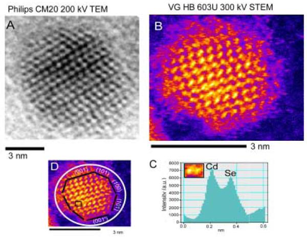
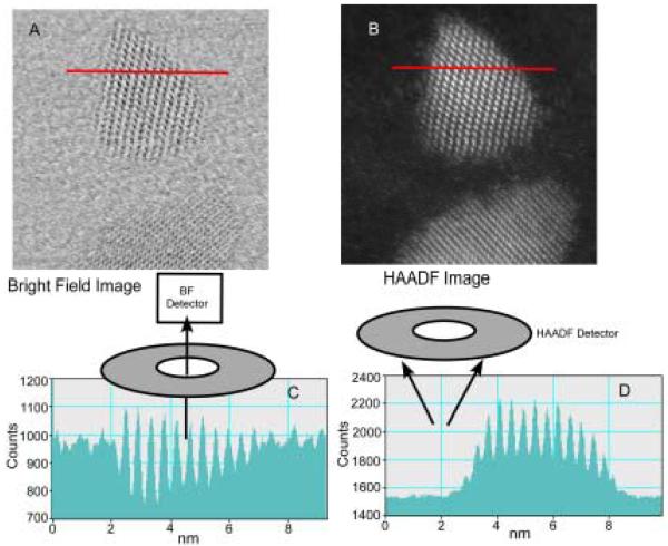
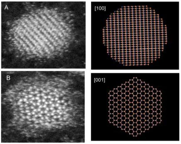
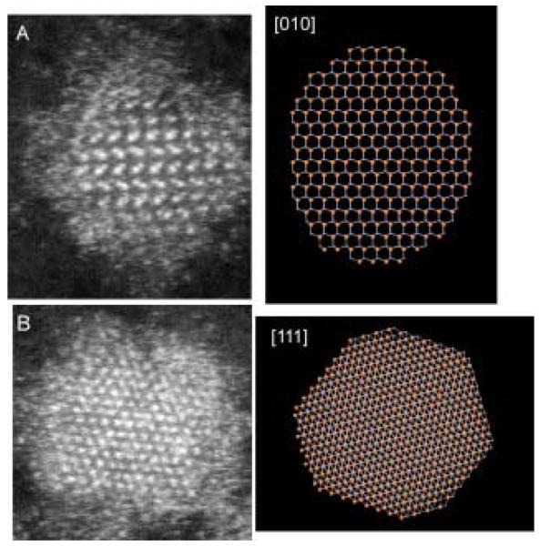
Abstract
Nanostructures, with their very large surface to volume ratio and their non-planar geometry, present an important challenge to surface scientists. New issues arise as to surface characterization, quantification and interface formation. This review summarizes the current state of the art in the synthesis, composition, surface and interface control of CdSe nanocrystal systems, one of the most studied and useful nanostructures.
Keywords: Cadmium, Selenium, Selenide, CdSe, nanocrystal, quantum dot, nanoparticle, surface, synthesis, electron microscopy, Z-STEM, RBS, alloy, core/shell, fluorescence, quantum yield, growth mechanism, expitaxy, spectroscopy
1.0 Introduction
1.1 Background
We are currently witnessing an explosion of research in nanoscale science, engineering, and biotechnology. As the nano-revolution proceeds, basic research is leading to the development of true nanotechnologies which have the potential to impact fields from health care and opto-electronics to energy and the environment. One particular type of nanostructure, semiconductor nanocrystals (also known as quantum dots), may ultimately be employed in technologies in each of these fields. For example, antibody-conjugated CdSe/ZnS core-shell nanocrystals have been used to detect respiratory syncytial virus.1 The high brightness of the quantum dots enables the virus to be detected in a matter of minutes, whereas the previous assay required 4 days. The ramification of this new technology is that anti-viral drugs can be given early in the infection when they are most effective, reducing hospitalizations and deaths. In the field of opto-electronics CdSe nanocrystals have been incorporated in light emitting diodes2-6 and it has been demonstrated that they can serve as the gain media in a laser.7, 8 Nanocrystals are also poised to play a role in solar energy conversion.9-14 A specific example is a device in which elongated CdSe nanocrystals (nanorods) are mixed with a conducting polymer and sandwiched between aluminum and indium tin oxide electrodes to create a device with a power conversion efficiency of 1.7 %.12 Nanocrystals may also have a positive impact on the environment, as it has been shown that they can be used to sequester CO2.15
The spark that ignited two decades of intense research in nanocrystal synthesis, properties, and applications was Louis Brus’ demonstration that quantum confinement of the photocreated electron-hole pair leads to the observed size dependent optical properties of CdSe nanocrystals.16, 17 While there have been studies on II-VI, III-V, and IV-VI nanocrystals, as well as metal oxide nanocrystals and others, CdSe remains the most thoroughly studied nanocrystal system. An early breakthrough came in 1993 when Murray, Norris and Bawendi developed the synthesis of CdS, CdSe, and CdTe nanocrystals by the high temperature pyrolysis of organometallic precursors.18 This afforded precise control of nanocrystal size and subsequent assignment of the electronic structure both experimentally and theoretically.19-23 Improvements in the synthesis followed which yielded monodisperse samples and eliminated the need for size selected separation for most applications.24 Near field scanning optical microscopy studies have determined the intrinsic nanocrystal linewidth and explained the phenomenon of single nanocrystal luminescence blinking.25 Structural studies have examined the hysterisis in the phase transition of wurtzite CdSe to rock salt CdSe nanocrystals.26 The ultrafast electronic dephasing,27 intraband transitions,28 and carrier dynamics29-33 have been determined by femtosecond spectroscopy. The molecular symmetry of CdSe nanocrystals have been determined and related to their Raman spectrum. Electron transport in thin films of CdSe nanocrystals has been studied.34 Numerous other studies have characterized the properties and explored the applications of CdSe nanocrystals. For further review see Alivisatos in the Journal of Physical Chemistry (1996) and others.35-38
1.2 Motivation
Nanocrystals present a quintessential problem for surface and interface science. Given that a nanocrystal is virtually all surface; its properties vary considerably as the crystal grows in size. By precisely controlling a nanocrystal’s size and surface its properties can be engineered. The most studied nanocrystal system and the focus of this report is CdSe. CdSe nanocrystals vary in size from ~1-11 nm and contain ten to ten thousand atoms. Through quantum confinement of the photocreated electron hole pair, the optical properties of the nanocrystal can be tuned by size.16 For example, a 1.2 nm nanocrystal will have 88% of its atoms on the surface and absorb light at 420 nm while an 8.5 nm nanocrystals consists of 20% surface atoms and absorbs light at 650 nm. Further, nanocrystals are chemically synthesized in an organic surfactant that not only passivates the surface, but also can control the growth rate of the nanocrystal, its size and shape.39 The surfactant/nanocrystal interface also controls the ultrafast carrier dynamics in the nanocrystal and the fluorescence quantum yield.29, 32, 40 Alternatively, the surface of the CdSe nanocrystal can be passivated with a second inorganic material, such as CdS, ZnS, or ZnSe to create a core-shell nanocrystal. When wrapped in a wider band gap material, the electron-hole pair is further confined and surface states are eliminated. If the interface between the two inorganics is perfect, a near unity quantum yield material may result.41 Here again characterization of the interface is crucial in order to engineer a quantum dot with desired properties.
Given their large surface to volume ratio and their non-planar geometry, nanocrystals present an important challenge to surface scientists. We have pioneered the application of two techniques that together are uniquely suited to study nanocrystals, nanocrystal surfaces and interfaces. These techniques are Rutherford backscattering spectroscopy (RBS) and atomic number-contrast scanning transmission electron microscopy (Z-STEM). RBS is a well known tool in surface science while Z-STEM has yielded unprecedented structural detail of solids, defects, and interfaces.42-46 When combined these techniques give information on nanocrystal composition, surface composition, surface ligand coverage, and nanocrystal structure, including interior, interfaces, and surfaces.
1.3 Objectives
There are several objectives for this report. In Section 2, Preparation of CdSe Nanocrystals and CdSe/ZnS Core/Shell Nanocrystals, the goal is to familiarize the reader with the various methods used to create CdSe nanocrystal structures and illustrate how the synthesis determines surface termination and nanocrystal shape. Section 3, Review of Surface Studies of CdSe Nanocrystals, provides a review of the literature concerning how CdSe surfaces have been previously characterized. In Section 4, Rutherford Backscattering Spectroscopy of CdSe and CdSe/ZnS Nanocrystals, we introduce the reader to RBS and illustrate how RBS can be used to explore the surface composition and coverage of surface passivating ligands. Section 5, Atomic Number-contrast Scanning Transmission Electron Microscopy (Z-STEM) of CdSe and CdSe/ZnS nanocrystals, introduces the reader to Z-STEM, illustrates how Z-STEM can be used for nanocrystal characterization for CdSe and CdSe/ZnS nanocrystals, and shows how Z-STEM allows the analysis of surface structure and even composition. Finally, in Section 6, Engineering a Biologically Active Nanocrystal, we focus on the biological applications of core/shell nanocrystals, the role the surface plays in determining biological activity, and how the surface can be characterized when engineering a biologically active nanocrystal.
2. Preparation of CdSe Nanocrystals and CdSe/ZnS Core/Shell Nanocrystals
The synthesis of CdSe nanocrystals has now been nearly perfected. Growing flawless nanocrystals is relatively easy because their length scale is so small there is simply not enough time during the growth process to introduce defects. This same tiny length scale, however, makes controlling the size and surface of nanocrystals a tremendous challenge. With current methods it is now possible to synthesize gram quantities of nanocrystals with exquisite control of size (± 2 Å). The procedures for fabricating nanocrystals have evolved over the past 25 years. Originally the synthesis of nanoparticles relied on salts as precursors and micellular methods to attempt to control size.47-49 These methods yielded poor samples as indicated by a lack of sharp absorption features. The emission spectra lacked any band-edge emission feature and consisted of a broad, intense, red-shifted “deep trap” emission originating from radiative recombination at defect sites and surface sites. A quantum leap in the quality and size control of CdSe nanocrystals came from Murray et al. with the development of high temperature pyrolysis of organometallic precursors in the surfactant trioctylphosphine oxide (TOPO).18 These methods are discussed below in Section 2.1.1. One of the reagents in these methods, dimethylcadmium ((CH3)2Cd), is air sensitive, pyrophoric and toxic. As a result, “greener” methodologies were explored and a methodology replacing dimethylcadmium with cadmium oxide (CdO) was developed.50 As an alternative to CdO, cadmium acetate Cd(CH3CO2)2 is also used.51, 52 These greener methods are discussed in section 2.2. Well made CdSe nanocrystals have very low quantum yields. For many applications, such as light emitting diodes and fluorescent labels in biology, bright nanocrystals are a highly desired commodity. Hines and Guyot-Sionnest were the first to synthesize core/shell nanocrystals: a CdSe nanocrystal wrapped in a ZnS shell (Figure 1). The ZnS shell passivates surface states eliminating traps and is a wider band-gap material further confining the electron-hole pair and resulting in efficient radiative recombination. Core/shell synthesis will be discussed in Section 2.3. Finally, Alivisatos and coworkers discovered how to make nanocrystals with different shapes: rods, tear drops, arrow heads, and tetrapods.39 These synthetic methods and a discussion of the role of individual surfaces in determining the shape of the crystal are discussed below in Section 2.4
Figure 1. Schematic of core and core/shell nanocrystal.
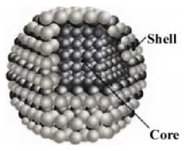
The core nanocrystal is coated with a wider band gap semiconductor to passivate the core surface in order to increase radiative recombination processes. Any uncoated surface could provide possible trap sites that result in non radiative recombination and a reduction in fluorescence quantum yield.
2.1 Pyrolysis of Organometallic Precursors
The first method to prepare highly monodisperse CdSe nanocrystals was presented by Murray, Norris, and Bawendi in 1993.18 (Section 2.1.1, the East Coast Method) The synthesis is based on the pyrolysis of organometallic reagents by injection into a hot coordinating solvent. The key to monodispersity is the separation of the nucleation and growth steps. The synthesis begins with the rapid injection of organometallic reagents into a hot coordinating solvent to produce a temporally discrete homogeneous nucleation. Slow growth and annealing in the coordinating solvent results in uniform surface derivatization and regularity in the core structure. Size selective precipitation provides powders of nearly monodisperse nanocrystals which can be dispersed in a variety of solvents. Improvements to this synthesis were made on the West Coast in the Alivisatos group which led to an improvement in the size distribution of the crystals.24 Another improvement came in 1998 when it was discovered that adding additional reagents as the synthesis progressed helped to “focus the size distribution” and enabled larger, more monodisperse CdSe nanocrystals to be grown (Section 2.1.3).53 Finally, the peculiarities of the coordinating solvent, trioctylphosphine oxide (TOPO) and its effect on the synthetic methodology are discussed in Section 2.1.4
2.1.1 The East Coast Method: TOP/TOPO
A typical experimental set up for nanocrystal synthesis is displayed in Figure 2. The solvent in this reaction is TOPO which is placed in the reaction vessel and heated to 300 °C. The TOPO is purchased from Alfa and usually purified by distillation prior to use. The cadmium precursor is dimethylcadmium, (CH3)2Cd, which is handled with standard airless techniques. The dimethyl cadmium is mixed with trioctylphosphine (TOP) as is selenium shot. These two solutions are combined and loaded into a syringe. The heat is removed from the reaction vessel and the reagent:TOP mixture is rapidly injected into the hot TOPO undergoing rapid stirring. Both organometallic reagents thermally degrade to reactive species in the hot solvent. The injection of the room temperature reagent solution causes a sudden decrease in temperature to 180 °C. Heating is resumed and the temperature is gradually raised to 230-260 °C. Aliquots of the reaction solution are removed from the reaction vessel at intervals of 5-10 minutes and absorption spectra are recorded to monitor the growth of the nanocrystals. The best quality samples are prepared over a period of a few hours in response to changes in the size distribution as determined by the width in the absorption features. The growth temperature is lowered in response to a spreading of the size distribution and increased when the growth stops. The nanocrystals are isolated by the addition of methanol which results in the flocculation of the nanocrystals. The flocculent is then separated from the supernatant by centrifugation, dispersed in 1-butanol and further centrifuged again to yield a solution of nanocrystals and a precipitate containing by products. Addition of methanol to the clear solution once again produces a flocculent which when rinsed in methanol and vacuum dried yields 300 mg of TOP/TOPO capped nanocrystals for 13.35 mmol of Cd.18 The characterization of the surface coverage will be discussed in Section 3. The fact that the surface is covered in an organic molecule means that the nanocrystals can be dispersed in organic solvents. As produced TOP/TOPO nanocrystals can be dissolved in non-polar solvents. Ligand exchange reactions can be performed to put polar groups on the surface of the nanocrystals and enable their dispersion in polar solvents.54, 55 As will be discussed in Section 6 surface modification with polar organic molecules is critical for nanocrystal applications in biological systems which are always in aqueous buffer solutions.
Figure 2. Typical experimental set up for the synthesis of nanocrystals.

A three neck flask is placed in a heating mantle and fitted with a thermocouple, a condenser, and a septum by which reagents are injected from a syringe. Argon or nitrogen can be purged from the top bump trap, through the three neck flask and out a needle placed through the septum.
2.1.2 The West Coast method: TBP/TOPO
In 1994, a year after the report of Murray et al. describing a powerful new method for synthesizing crystalline, monodisperse, size tunable CdSe nanocrystals, Bowen-Katari, Colvin and Alivisatos reported an improvement in the procedure which eliminated the need for size-selected precipitation, which is a time consuming, wasteful, and tedious procedure.24 The principal difference is the temperature of the injection, which affects the time evolution of the nanocrystal growth as well as the crystallinity and shape of the nanocrystals. A second difference is the use of tributylphosphine (TBP) to coordinate to Se instead of the use of TOP. The use of TBP instead of TOP results in a low coverage of Se surface atoms, as TBP is more labile at 350 °C. In this preparation, 99% TOPO and TBP were used as received from Aldrich. Se (60 mesh powder) was dissolved in TBP and followed by the addition of dimethylcadmium. The solution is then diluted 4:1 with TBP and the reaction vessel TOPO was heated to ~350 °C. It is found that differences in temperature of less than 1 °C can change both the average size and the quality of the size distribution. When the temperature had stabilized, the reagent solution was rapidly injected. The solution was removed from heat and allowed to cool under argon, which prevents any oxidation of the nanocrystal surface. To recover nanocrystals from the solid, room temperature TOPO mixture, methanol was added to dissolve the TOPO and precipitate the nanocrystals which were then recovered by filtration. To make nanocrystals with an absorption maximum larger than 580 nm, the reaction was cooled from 350 °C to 320 °C and the nanocrystals were allowed to grow (here again the size was monitored by drawing aliquots from solution and monitoring the absorption spectra). Using this growth method the initial tight control of size distribution was lost. This can be overcome by the addition of additional reagent solution to “focus” the size distribution, which is discussed below in section 2.1.3.
2.1.3 Size-Focusing
In 1998 Peng, Wickham and Alivisatos published a kinetic study of nanocrystal growth and demonstrated how the nanocrystal size can be “focused” through the addition of monomer reagents (the initial reagent solution) during the course of the reaction.53 The strategy was designed to overcome Ostwald ripening, or “defocusing” of the size distribution. Ostwald ripening occurs when smaller nanocrystals in the distribution dissolve and become smaller and the monomers released allow the larger nanocrystals in the solution to grow further, subsequently broadening the size distribution.
The “focusing” argument is as follows: at a given concentration of monomer in the reaction solution and assuming diffusion is the rate limiting step for growth, the size dependent growth rate can be obtained by considering the Gibbs-Thompson equation:56
| (2.1) |
Sr and Sb are the solubility of the nanocrystal and the corresponding bulk solid, σ is the specific surface energy, r is the radius of the nanocrystal, Vm is the molar volume of the materials, R is the gas constant and T is the temperature. If 2σVm/rRT << 1 then the diffusion controlled rate of growth of the nanocrystal of a size r is:
| (2.2) |
In the above equation K is a constant proportional to the diffusion constant of the monomer. δ is the thickness of the diffusion layer. At a fixed concentration, r* is the critical radius for which the solubility of the nanocrystal is exactly equal to the concentration of monomer reagent in solution (zero growth rate). At any monomer concentration there is a critical size which is at equilibrium. Nanocrystals smaller than r* dissolve while larger nanocrystals grow at rates strongly dependent on size. When the nanocrystals in solution are slightly larger than the critical radius the size distribution “focuses”. For these conditions, small nanocrystals grow faster than large ones. When the monomer reagent is used up the critical size becomes larger than the average size and Ostwald ripening occurs. The nanocrystal size distribution can be partially recovered by adding more monomer at this time. By varying the initial monomer concentration the focusing time as well as the focused size varies. Focusing times and sizes are determined by experiment. Peng, Wickham and Alivisatos note that in an actual experiment the concentration of the monomer changes continuously so that r* and the relative growth rates of the various sizes are also changing. Peng et al. suggest the optimum way to synthesize narrow size distributions for all desired sizes is to continuously monitor and adjust the monomer reagent concentrations. To our knowledge automation of this procedure has not yet been implemented. Nevertheless, this size focusing methodology provides highly monodisperse size distributions even at larger nanocrystal sizes, which were previously problematic.
2.1.4 The TOPO Story
The choice of trioctylphosphine oxide (TOPO) as the coordinating solvent allows the reaction to take place above the nucleation temperature (since TOPO has a high boiling point) and, as we will discuss extensively below, passivates the surface of the nanocrystal such that nanocrystals do not agglomerate. Further, the TOPO on the surface allows the nanocrystals to be soluble in organic solvents or dispersed in a polymer film. Clearly, Murray’s choice of TOPO was one key to revolutionizing the synthesis. However, it was discovered early on that there were peculiarities in the TOPO. As an example 90 % TOPO (technical grade) from Aldrich produced nanocrystals with sharp absorption features whereas 99 % TOPO yielded nanocrystals with a broad absorption onset and no sharp features. It became apparent that there was an impurity in the TOPO that was affecting the synthesis in a positive way. Peng et al. first postulated that the important impurity was a phosphonic acid.39 The impurity was also variable, leading to fluctuations in the synthesis from one batch of TOPO to the next. This ultimately triggered an evolution in the synthetic methodology used in our laboratory.57 When we found a batch of TOPO that yielded high quality nanocrystals we would buy the entire lot number (several kilos of TOPO). This strategy ultimately failed when all the current batches of TOPO from all suppliers failed to yield high quality nanocrystals. At this point we continued using technical grade TOPO, but added co-solvents that improved yield and quality of the nanocrystals synthesized.58 The first co-solvent was dodecylphosphonic acid (DPA) which supplements the unknown impurity and slows the nucleation process so that the size distribution is not as distorted as the system rapidly cools to the growth temperature. Using DPA helps not only with the quality of the nanocrystals produced but also with the quantity. Large batches of nanocrystals with a narrow dispersity are produced since larger volumes of reagents can be nucleated while maintaining a sharp UV-Vis absorption spectrum.
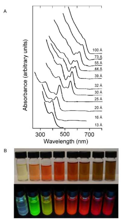
The second co-solvent, hexadecylamine (HDA), provides resistance to Ostwald ripening.59, 60 Nanocrystals grown in TOPO/DPA/HDA maintain a narrow dispersity for many hours (~7 hr) at growth temperatures. The use of only TOPO and DPA yields major broadening of the band edge absorption, and hence a large polydispersity, in less than an hour. The surface-bound HDA must provide a lower overall energy for the nanocrystal than does a larger surface face. Equivalently, if the larger surface face were more stable than a smaller face with HDA, then Ostwald ripening would be observed. The mechanism of Ostwald ripening is noticeably inhibited, since the band edge absorption does not broaden even for extended periods at the growth temperature (Figure 3).61
Figure 3. Series of CdSe nanocrystals synthesized in TOPO/HDA/DPA.
The typical CdSe absorption spectrum exhibits a sharp absorption onset followed by multiple electronic states that are visible in the spectra, as shown in Figure 3A. The absorption continuum allows for several sizes of nanocrystals to be optically excited by a single wavelength. Figure 3B is an image of a representative sample of CdSe cores under room lights (TOP) and under UV illumination (BOTTOM).62
It is further observed that a balance between TOPO and HDA is required. Truly unique is the almost complete separation of the activity of both co-solvents, considering that not only is a single reaction being modified, but a single reagent is being targeted. This would seem to lend support to the supposition that the DPA truly influences the cadmium precursor, while the HDA affects the cadmium once incorporated onto the nanocrystal surface. Comparison of TBP:TOPO and TOPO/DPA/HDA nanocrystals by Z-STEM (Atomic Number Contrast Scannin g Transmission Electron Microscopy) is presented below in Section 5.
2.2 “Greener” Methods for CdSe Nanocrystal Synthesis
The cadmium precursor for all of the synthesis described above is dimethylcadmium, (CH3)2Cd. This reagent is pyrophoric and therefore requires standard airless techniques (Schlenk lines and glove boxes). This is fine for a research setting, but difficult for the standard undergraduate laboratory, where fabrication and characterization of CdSe nanocrystals provides a beautiful, “real world” application of the quantum mechanical concept of the particle in a box.62 Further, (CH3)2Cd is expensive and is toxic. Many initially believe dimethylcadmium to have a similar toxicity (LD50 or Lethal Dose, 50%) to dimethylmercury, which in at least one instance has caused a laboratory fatality. Fortunately, for two reasons, dimethylcadmium is actually much less toxic. First, cadmium is bound by the scavenging enzyme, metallothionein. The bound cadmium is then stored in the liver until cell death, then is transported to the kidney for the life of the individual. This explains the low time weighted average (TWA) for cadmium compounds in the MSDS. Even though (CH3)2Cd may cross the blood brain barrier it is bioactive; therefore the mechanisms already in place within the body for dealing with heavy metals are effective. This is unlike alkyl mercury compounds, which have no removal mechanism and do damage in the brain. As with any heavy metal there will be illness and possible morbidity from a large acute dose. Concentrations over 200 μg per kg body mass lead to toxic effects. At these concentrations, cadmium begins to replace copper and zinc in various metallozymes rendering them inactive (e.g. cytochrome P60 and DNA binding proteins). The second reason was an oversight in early testing which over predicted cadmium toxicity. In testing cadmium as an alternative for the anticorrosive tin in “tin cans”, cadmium was found to have a very low LD50. Later work, however, showed the chicken embryos used for testing overproduced metallothionein, which lead to a copper deficiency and fetal death. So although dimethylcadmium is not as toxic as dimethylmercury, it is advisable to use a handling program in accordance with exposure, as should be practiced when handling any heavy metal (e.g. meticulous glove use and require yearly screenings for heavy users). Finally, an inhalation hazard exists. The fine CdO particles from the rapid degradation of Cd(CH3)2 in air in large doses can cause respiratory distress or failure as any fine particulate. Inhalation symptoms usually appear within 1-8 hours of exposure.62
Of course developing new synthetic methodologies which employ a different precursor can eliminate the fire hazard (Cd(CH3)2 is pyrophoric) and some of the health hazard. In large part, the nanocrystal community has headed in this direction. A seminal paper in this regard is from Peng & Peng who put forward a synthetic methodology which uses CdO as the cadmium precursor.50 In this one pot approach, CdO, TOPO and either hexylphosphonic acid (HPA) or tetradecylphosphonic acid (TDPA) were loaded into a three neck flask. At temperatures above 270 °C, the phosphonic acid complexes with the CdO forming a clear and colorless solution. After the formation of the colorless cadmium phosphonate complex, TBP:Se was then injected which initiates the formation of nanocrystals. The authors found that not only can high quality CdSe nanocrystals be produced by this method but when the Se was replaced by Te or S high quality CdTe and CdS nanocrystals can also be produced. Peng et al. postulate that CdO works well as a precursor due to its low stability relative to the phosphonates in comparison to other precursor candidates such as CdCl2.63
CdO is not the only alternative to dimethylcadmium being employed in nanocrystal synthesis. Weller and co-workers developed a synthetic methodology using cadmium acetate Cd(CH3CO2)2 as the precursor.51 In this method a stock selenium solution of TOP:Se is added to a mixture of TOPO:HDA:TDPA at 120°C This is then heated to 300°C to which a stock solution of cadmium acetate in TOP is rapidly injected. Both the cadmium and selenium stock solutions are stored inside a glove box under nitrogen atmosphere. While some air free techniques are still required, these “greener” methods are certainly more favorable for classroom and large scale industrial settings. Indeed, a recent method for synthesizing CdS and CdSe is so “green” it uses vegetable oil (oleic acid) to complex Cd from CdO.64 In this method, TOPO is replaced with the noncoordinating solvent octadecene.
2.3 Core/Shell Nanocrystals
The methodologies described above indicate that CdSe nanocrystals can be prepared that are nearly monodisperse, can be grown to a desired size over a large range, have good crystallinity and desired surface properties. For several applications though, it is desired that the nanocrystals have a high luminescence quantum yield. For the CdSe nanocrystal methodologies described above the quantum yields range between 1-15 %. Indeed, well made large CdSe nanocrystals register no fluorescence. The simplest explanation of this is because of the rapid trapping of carriers to surface sites.29
In 1996 Hines and Guyot-Sionnest made the important discovery that the luminescence from CdSe nanocrystals can be substantially improved by growing heteroepitaxally an inorganic shell of a wide band gap semiconductor, in this case ZnS, around the nanocrystal.65 This work opened the path that led directly to two key publications in Science exploiting the properties of CdSe/ZnS nanocrystals for biological application and initiated that field.55, 66 This will be discussed further in Section 6. Other groups soon followed in developing methods for the synthesis of core/shell nanocrystals.52, 60, 67-72 Indeed, it is now possible to synthesize nearly unity quantum yield materials.41 In this report we will show how a synergistic combination of synthesis, RBS, and Z-STEM has led to these materials. In this section we review a few of the different methods for fabricating core/shell nanocrystals.
The first method for fabrication ZnS –capped CdSe nanocrystals presented by Hines and Guyot-Sionnest used all organometallic reagents and was a one pot synthesis. Initially CdSe nanocrystals were made by the addition of a TOP:Se and Cd solution to 350 °C TOPO. The reaction mixture was allowed to cool and when it reached 300 °C the Zn/S/TOP reagent solution was added. The Zn/S/TOP stock solution was prepared using (TMS)2S (bis(trimethylsilyl)sulfide) and (CH3)2Cd as the cadmium and sulfur precursors. The Zn/S/TOP reagent solution was injected in five half milliliter proportions at intervals of 20 seconds. The Zn/S/TOP solution was added at lower temperature and in steps in order to avoid nucleation of ZnS nanocrystals. The mole ratio of injected reagents was 1:4 CdSe:ZnS. The reaction mixture was cooled to 100 °C and stirred for 1 hour. The nanocrystals were purified by precipitation with anhydrous methanol, collected by centrifugation and washed three times with anhydrous methanol. Transmission electron microscopy (TEM) and X-Ray photoelectron spectroscopy (XPS) studies indicated that this method produces CdSe/ZnS nanocrystals. The fluorescent quantum yield of these particles was 50% and the broad surface-trapping emission feature was eliminated from the fluorescence spectrum. Fluorescence lifetime measurements determined by the phase method showed a four component lifetime as follows: 8.5%, 160 ns, 53%, 26 ns 37%, 12 ns, and 1.5% 1.5 ns. Hines and Guyot-Sionnest used TEM to characterize the particles. We will see below in Section 5 how Z-STEM can reveal additional information on core/shell structures and how that relates to the fluorescence quantum yield of the material.
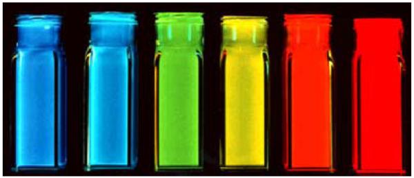
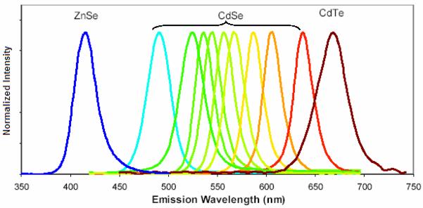
Shortly following the paper of Hines and Guyot-Sionnest, Dabbousi et al. presented their work on the synthesis and characterization of a series of CdSe/ZnS core/shell nanocrystals in which the core size varied from 23 to 55 Å.67 The quantum yields of their materials ranged from 30-50%. The wide spectral range of the emission in these materials is shown below in Figure 4. The synthetic methodology of Dabbousi et al. was a two-pot synthesis.67 The CdSe nanocrystals were first synthesized by the East Coast TOP/TOPO method as described above in Section 2.1.1.18 These nanocrystals were isolated as powders and then redispersed in hexanes. These dots were added to a TOP/TOPO solution at 60 °C via syringe and the hexane solvent was evaporated. The Zn and S precursors were diethylzinc (ZnEt2) and (TMS)2S, respectively. The amount of precursors needed to grow a shell of desired thickness was calculated based on the ratio of the shell volume to the core assuming a spherical CdSe nanocrystal. Equimolar amounts of the Zn and S precursors were dissolved in TOP inside a glove box, loaded into a syringe, and transferred to an addition funnel attached to the reaction flask. The reaction flask containing the CdSe nanocrystals, TOP, and TOPO was heated and the Zn and S precursors were added dropwise to a vigorously stirring reaction mixture over a period of 5-10 min. The temperature of the addition varied depending on the size of the core CdSe. For 23 Å cores the reaction mixture was held at 140 °C whereas for 55 Å cores the reaction mixture was heated to 220 °C. After addition, the mixture was cooled to 90 °C and continued stirring for several hours. Butanol was added to keep the TOPO from solidifying. The ZnS coated CdSe particles were stored in TOPO to ensure surface passivation. They were recovered as powders by precipitation in methanol. Dabbousi et al. characterized their core/shells by wavelength dispersive X-ray spectroscopy (WDS), XPS, TEM, small-angle X-ray scattering (SAXS) and wide-angle X-ray scattering (WAXS) as well as standard optical characterization by absorbance and fluorescence.67 TEM, SAXS, and WDS demonstrated an increase in the size of the core/shells with increasing Zn:Cd ratios as well as an increase in the size distribution and aspect ratio. WAXS probed the internal structure and indicates that at very high coverage the ZnS shell retains its bulk lattice parameter. At low coverage the ZnS shell appears to be epitaxial but Dabbousi et al. concluded that at high coverage the shell is partially epitaxial but probably contains defects to accommodate the 12% lattice mismatch between ZnS and CdSe.67
Figure 4. Series of highly fluorescent CdSe/ZnS core/shell nanocrystals (Bawendi).
The emission can be tuned from blue through red depending upon the size of the core CdSe nanocrystal.
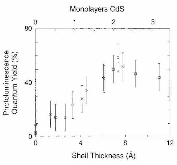
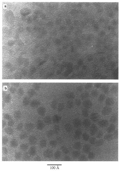
Peng et al. also published the fabrication and characterization of core/shell nanocrystals in 1997 but their system was CdSe capped by CdS.71 They fabricated core/shells from three different sizes of CdSe cores: 23 Å, 34 Å and 39 Å. Their method is also a two pot synthesis. The synthesis of the cores follows the procedure outlined above in Section 2.1.2. The stock solution for shell growth uses (CH 3)2Cd for the cadmium precursor and (TMS)2S for the sulfur precursor. These are dissolved in TBP with an ultimate Cd:S ratio of 1.0:2.1. To grow core/shells CdSe nanocrystals are placed in a three neck reaction flask to which pyridine is added. The nanocrystals readily dissolve in the pyridine which is then refluxed over night. The solution was heated to 100 °C and the shell solution added dropwise at a rate of approximately 1 drop per second. Stopping the CdS addition and removing the heating completed the growth. Dodecylamine was added to the reaction solution at room temperature until the nanocrystals precipitated. The absorption spectra indicated a red shift for the core/shells as compared to the cores. The photoluminescence quantum yield increased with increasing shell thickness, peaking at 50% for all samples at ~7 Å shell thickness, (Figure 5). These core/shells were further analyzed by XPS, TEM, and XRD to demonstrate that a shell is indeed grown as opposed to forming a CdSxSe1-x alloy. A comparison of the 34 Å cores and the core/shells with a shell thickness of 9 Å is shown in Figure 6. It is clear from this comparison that the core/shells are bigger than the cores. However in traditional high-resolution TEM (HRTEM) the shell cannot be distinguished from the shell, therefore the uniformity of the shell coverage cannot be assessed. As we will see below in Section 5 Z-STEM allows for just such an analysis.
Figure 5. Increasing fluorescence quantum yield as a function of shell thickness for CdSe/CdS core shell nanocrystals.
The fluorescent quantum yield peaks for a shell thickness of 7Å. The degradation of the fluorescent quantum yield is likely the result of the formation of CdS nanocrystal which will absorb light but not contribute to the desired luminescence.71
Figure 6. Transmission electron microscopy image comparing 34 Å cores to core/shells with a shell thickness of 9Å.
While a difference in size is clearly observable, details concerning the uniformity of shell coverage cannot be determined by HRTEM.71
Just as “greener” methods were devised for the synthesis of CdSe nanocrystals, Weller and coworkers applied the same principles to the growth of CdSe/CdS nanocrystals in a one-pot approach.52 The procedure begins with the synthesis of CdSe nanocrystals from Cd(CH3CO2)2 and TOP:Se precursors as described above in section 2.2. To make the core/shells a reaction flask containing a freshly prepared crude solution of CdSe nanocrystals was heated to 140 °C. H2S gas was injected above the solution and not bubbled through the reaction solution. The reaction mixture absorbed the H2S during stirring for a half an hour. The temperature of the reaction mixture was then decreased to 100 °C and stirred an additional hour. The mixture was cooled to 50 °C at which point chloroform was added to the solution to prevent solidification of the TOPO and HDA when the mixture was cooled to room temperature. The nanocrystal solution was injected through a 0.2 μm syringe filter followed by isolation of the nanocrystals by precipitation with methanol. The CdSe/CdS core shells produced by this method have narrow photoluminescence spectra (FWHM ~27-35 nm) with quantum yields as high as 50-85%. However, Weller and co-workers do not rule out that a CdSxSe1-x alloy or gradient composition is formed. Below in Section 5 we will see how this dilemma can be addressed with Z-STEM.
2.4 Unique Shapes
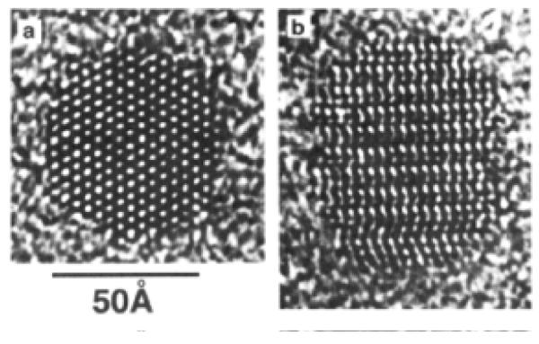
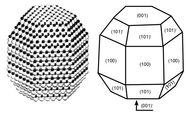
Before describing unique nanocrystal shapes, it is imperative to present the standard shape of CdSe nanocrystals prepared by the synthetic methods presented above in Section 2.1. The defining work on the determination of CdSe nanocrystal shape and symmetry was presented by Shiang et al.73 The shape of the nanocrystal is revealed in the impressive HRTEM images obtained by Kadavanich (Figure 7) which clearly show that the nanocrystals are facetted and slightly elongated in the direction of the C3v symmetry axis. The shape of the nanocrystal can be described as a hexagonal prism capped by two frustrums (Figure 8).74 Indeed Raman depolarization studies confirmed the assignment of CdSe nanocrystals to the C3v point group. The elongation of the nanocrystals varies with size: small nanocrystals have an aspect ratio of ~1.1:1 while larger nanocrystals have a ratio of ~1.4:1.75 The model presented in Figure 8 is for a 1:1 Cd:Se stoichiometric nanocrystal. Implicit in this description of the shape of the nanocrystal is that the terminating top and bottom planes consist solely of Se (001′) and Cd (001). This shape dictates an intrinsic dipole moment which was ultimately observed by Guyot-Sionnest.76 We will see in Section 4 that RBS analysis shows these nanocrystals are indeed not stoichiometric.
Figure 7. HRTEM images of 60 Å CdSe nanocrystals parallel and perpendicular to the C3 axis.
Faceting and elongation along the C3 axis a clearly visible (Figure 7a). Additionally, zinc blende stacking faults are visible running perpendicular to the C3 axis (Figure 7b).
Figure 8. Three dimensional shape of CdSe nanocrystals determined from HRTEM images.
Certain facets are rich in either Cd or Se which results in varied reactivity for certain surfaces.
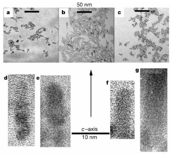
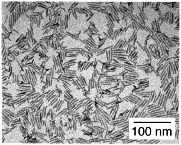
Control of CdSe nanocrystal shape was first demonstrated in CdSe nanorods that could be grown with different aspect ratios (Figure 9).39 It is possible to control the shape of CdSe nanocrystals because of the anisotropic growth of the wurtzite structure. When the system is kinetically driven at extremely high monomer concentrations, the C axis of the wurtzite structure is the preferred growth direction. However, if pure TOPO is used as the surfactant in combination with extremely high monomer concentrations the growth is too fast resulting in insoluble and unprocessable rods. Technical grade TOPO contains impurities which slow the growth.77 The impurities present that are likely to slow the growth by binding strongly to cadmium atoms are alkyl phosphonic and phosphinic acids. Peng et al. discovered that by adding a molecule that bound more tightly to Cd than TOPO, they could control the growth kinetics and produce nanorods.39 Hexylphosphonic acid (HPA) was chosen to simulate the impurities found in technical grade TOPO. The synthesis generally follows the TOPO/TBP scheme outlined above. With small amounts of HPA added to the TOPO (1.5 % and 3 % by weight) spherical nanocrystals result. At higher amounts of HPA (5 %, 10 %, and 15 %) nanorods result. The aspect ratio, size, and growth rate of the nanorods can be systematically controlled by varying the reaction time, the injection and growth temperatures, and the number of injections.
Figure 9. CdSe Nanorods.
HRTEM images of CdSe grown with different aspect ratios, demonstrating the ability to control the growth along the C3 axis.39
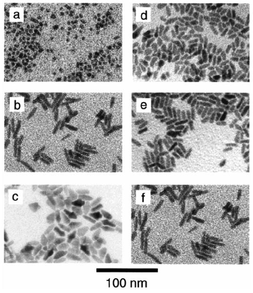
Manna et al. extended the methodology of doping pure TOPO with HPA to create a variety of nanocrystal shapes.78 By controlling the ratio of the surfactants, the injection volumes, and the time-dependent monomer concentrations they produced arrows, teardrops, tetrapods and extremely large aspect ratio (30:1) nanorods. The argument for the origin of shape control is generally as follows: during the growth of the nanocrystals, the surfactants dynamically adsorb to the growing crystallites, allowing atoms to add and subtract for high crystallinity. The surfactant enables the growing crystallite to anneal, resulting in good crystallinity while at the same time preventing aggregation. The growth kinetics can be controlled by varying the time-dependent monomer concentration through the initial injection volume and additional injections, and by the addition of a phosphonic acid, which allows the (001′) surface to grow faster relative to the other surfaces. An example of this principle is shown in Figure 10.
Figure 10. HRTEM images of CdSe nanocrystals demonstrating shape control.
By controlling the ratio of the surfactants, the injection volume, and the time-dependent monomer concentration different shapes and sizes can be obtained. Figures a-c demonstrate the effect of surfactant. The surfactant ratio was increased for (a) 8 to (b) 20 to (c) 60% HPA in TOPO. Figures d-f illustrate the effect of injection volume. The injection volumes used were (d) 1.0, (e) 1.5, and (f) 2.0 ml.78
At concentrations of HPA less than 10% a roughly spherical shape results. At a concentration of HPA of 20 % high aspect ratio rods are formed (Figure 10b). With a HPA concentration of 60% arrows are formed (Figure 10c). Figures d-f illustrate the effect of injection volume. For a fixed HPA concentration of 20% larger aspect ratio rods are obtained by increasing the injection volume. Nanorods with an aspect ratio of 10:1 can be obtained by additional injections during the growth phase (Figure 11).
Figure 11. TEM images of nanorods.
The extended rods are obtained by adding additional reagent during the growth. The arms are believed to extend from a zinc blend core.78
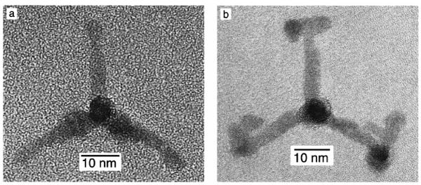
Teardrops (tadpoles) result with a slow initial injection rate and additional slow injections during the course of the reaction. The crystals that were pure wurtzite grew significantly more on the (001′) face, forming the teardrop shape. Finally, all of the synthesis that form nanorods contained some percentage of tetrapods (Figure 12) which can be isolated by size-selected precipitation. The tetrapods are crystalline both in the center and the arms.
Figure 12. HRTEM images of tetrapods.
The tetrapods are formed as a by product in the synthesis of nanorods and separated by size-selected precipitation. The asymmetric structure of the nanocrystal can be used to form self assembled ordered structures for device application.78
The variation of nanocrystal shapes is an intriguing manifestation of surface science. As discussed above, wurtzite CdSe nanocrystals have differing top and bottom faces i.e. the (001′) is anion rich. If we examine a model from Manna et al. (Figure 13), it can be seen that Cd atoms on the (001) face have one dangling bond while the Cd atoms on the (001′) face have three dangling bonds.78 In the presence of HPA the relative growth rate of the (001′) face is much greater than the other faces. The formation of arrows at large HPA concentration unequivocally points to unidirectional growth. The important role of HPA was confirmed by Peng and Peng who claim that its role is to enable the high monomer concentration necessary for growth of nanorods.63
Figure 13. Schematic of dangling bonds.
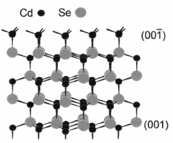
Demonstration of the types of dangling bonds available for reaction for the different growth faces of wurtzite CdSe. On the (001) face, Cd atoms have only one dangling bond, while on the (001′) face Cd atoms have three dangling bonds.78
2.5 Practical Guide for the Synthesis of CdSe Nanocrystals
The following reagents and methods are used for the synthesis of CdSe nanocrystals in our laboratory. Tri-n-octylphosphine oxide (TOPO, 90% tech. grade), hexadecylamine (HDA, 90% tech. grade) are purchased from Aldrich and used as received. CdO (99.999% Puratrem), tri-n-butylphosphine (TBP, 97%) and selenium powder (200 mesh) are purchased from Strem and used as received. Dodecylphosphonic acid (DPA) is synthesized via the Abruzov reaction from triethylphosphite and 1-dodecylbromide followed by acidification with concentrated HCl and recrystallization from cold ethyl acetate. All other solvents were HPLC grade and purchased from Fisher Scientific unless otherwise noted.
A 1.0 M stock solution of selenium in TBP is produced by dissolving 7.896 g of selenium powder in 100 ml of TBP and is kept in a glovebox under nitrogen. 30 ml of this solution is mixed with 120 ml of TBP to produce a 0.2 M working solution which is stored in a sealed bottle with a Teflon-lined rubber septum outside the glovebox. 0.128 g of CdO, 0.496 g of DPA, 6g of HDA and 4 g of TOPO are placed in a 100 ml three-neck flask with a Teflon-coated magnetic stir bar. A rubber septum is placed over one of the flask openings to allow the injection of precursors. A rotovap bump-trap fitted with a gas adapter is placed in the middle opening while a temperature probe fitted with an adapter is placed on the remaining opening. Argon is then purged through the flask from the bump-trap out through a needle placed in the rubber septum while the solution is heated to 150 °C. At 150 °C, the purge needle is removed and the solution is allowed to heat to 320 °C. The CdO converts to cadmium phosphonate, yielding a clear reaction solution. 5 ml of the 0.2 M Se:TBP solution is drawn up in a syringe and fitted with a 12 gauge needle. Immediately prior to the Se:TBP injection, the reaction temperature controller is set to 270 °C and the heating mantle is lowered from the reaction flask. The Se:TBP is quickly and forcefully injected into the reaction solution at 315 °C which will drop the reaction temperature to about 270 °C. The heating mantle is raised back under the reaction flask and the reaction is allowed to proceed until the desired size of nanocrystal is achieved. This can be monitored by UV-Vis spectroscopy by pulling aliquots using a glass syringe. The reaction can be stopped by lowering the heating mantle and using compressed air to drop the reaction temperature below 100 °C. A careful injection of 10 – 20 ml of butanol can also be used to stop the reaction quickly.
The nanocrystals are cleaned in three steps. The first step is by precipitation in methanol which serves to remove excess TBP and TOPO. The second step involves the addition of just enough octanol to cover the pellet from the previous step and is mixed into a cloudy suspension. This suspension is again centrifuged until the supernatant is clear. The pellet on the bottom is a mixture of HDA and unreacted cadmium phosphonate. The supernatant is then carefully decanted into a new via. The nanocrystals are then precipitated with methanol and a few drops of ethyl acetate followed by centrifugation.
3. Review of Surface Studies of CdSe Nanocrystals
Studies of surface bonding, surface chemistry, and surface reconstruction have dominated the field of surface science for the past 50 years. Experimental techniques have been designed for, and evolved around, planar structures. Indeed, the electronic properties of the surface 2D electron gas was the first low dimensional problem studied, illustrating changes in properties determined by lower dimensionality. Nevertheless, surface science experimental tools are not well suited for the studies of nanocrystals; hence there is a limited amount of literature concerning the application of surface science tools to chemically synthesized quantum dots. Of course this is a most significant omission since nanostructures are solids in which the surface is more dominant than in any other structure. Here we review the experimental studies which have analyzed CdSe nanocrystal surfaces.
3.1 X-Ray Photoelectron Spectroscopy
X-ray photoelectron spectroscopy (XPS) is a critical tool in the analysis of surfaces. XPS was developed in the mid 1960’s by K. Siegbahn and his research group and was awarded the Nobel Prize for Physics in 1981 for his work in XPS. The phenomenon is based on the photoelectric effect outlined by Einstein in 1905 where impinging photons cause the ejection of electrons from a surface. For XPS, Al Kα (1486.6 eV) or Mg Kα (1253.6 eV) are often the photon energies of choice. Other X-ray lines can also be chosen such as Ti Kα (2040 eV). The XPS technique is highly surface specific due to the short range of the photoelectrons that are excited from the solid. The energy of the photoelectrons leaving the sample is determined using a high resolution electron analyzer and gives a spectrum with a series of photoelectron peaks. The binding energy of the peaks is characteristic of each element. The peak areas can be used (with appropriate sensitivity factors) to determine the composition of the material’s surface. The shape of each peak and the binding energy can be slightly altered by the chemical state of the emitting atom. Hence XPS can provide chemical bonding information as well. XPS is not sensitive to hydrogen or helium, but can detect all other elements.
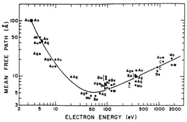
XPS is traditionally carried out in UHV conditions to maintain a pristine surface. The surface sensitivity is governed by the electron escape curve shown below in Figure 14.79 The escape depth of the electrons corresponds to the depth sampled. In XPS of quantum dots, the escape depth can be comparable to the size of the nanocrystal, which can complicate data analysis. In the simplest approximation, the final energy of the electron is given by:
| (3.1) |
where the binding energy corresponds to a specific atom and contains information on the chemical binding. The “escape curve” and this simple equation also illustrate the growing use of synchrotrons as x-ray sources. These variable energy sources allow variation of the incident energy to control the depth sampled.
Figure 14. Electron escape curve.
Graph of the mean free path in Å verses electron energy for surface sensitivity in XPS.79
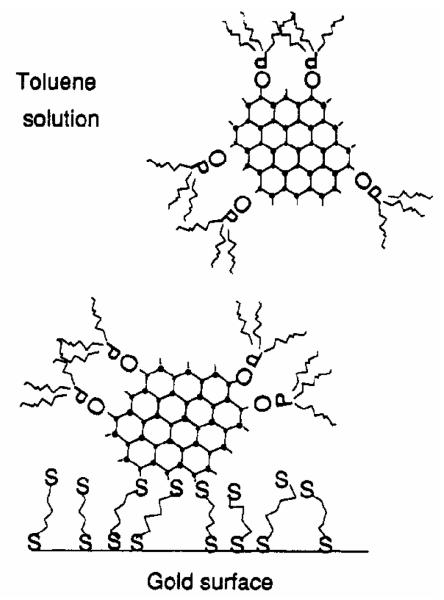
One of the earliest and most extensive studies of the nature of the CdSe nanocrystal surfaces was an XPS study by Katari, Colvin, and Alivisatos.24 This is also one of the few examples of a traditional surface science technique applied to CdSe nanocrystals. In this work, the TBP/TOPO method (Section 2.1.2) was used to fabricate the nanocrystals. In order to perform an XPS experiment, the nanocrystals must be attached to a conducting surface so they do not charge during the experiment. The nanocrystals must also be attached at a uniform distance which must be small. Further, the nanocrystals must be in a single layer without bunching or stacking. Finally the samples must be robust. To meet these requirements the authors employed the method of Colvin et al. in which the nanocrystals are covalently attached to a gold surface using hexanedithiol (Figure 15).80
Figure 15. Sample geometry for performing XPS on CdSe nanocrystals.
The nanocrystals are tied off to a gold surface using hexane dithiol as a “molecular glue”.
In this method, hexanedithiol is self-assembled on ion-etched gold evaporated onto glass slides. The slides are then soaked in a solution of TOPO coated nanocrystals which covalently bind to the sulfur atom of the hexanedithiol. Empirically it was determined that hexanedithiol has the optimal chain length. Longer alkanethiols have the potential to loop, leaving no site for nanocrystal attachment, while shorter chains do not bind strongly enough to the gold to bind nanocrystals to the surface. In addition to attaching nanocrystals to gold surfaces Bowen-Katari et al. also attached CdSe nanocrystals to doped silicon surfaces. Acid cleaned Si (111) wafers were placed in a boiling solution of 10 g of distilled water and 10 g of (3-mercaptopropyl)trimethoxysilane in 400 g of 2-propanol. This process was repeated three times and then the wafers sat in a nanocrystal solution overnight. In the case of both the gold and silicon substrates, the samples were stored under nitrogen to avoid oxidation of the nanocrystal surfaces. FTIR on these samples showed the presence of TOPO on the nanocrystals and Raman spectroscopy confirmed the presence of nanocrystals on the surfaces. RBS on these samples indicated roughly one-sixth a monolayer of coverage. The above methodologies for creating monolayers of nanocrystals attached to surfaces lend themselves to other “traditional” surface science experiments.
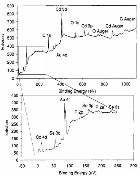
A typical low resolution XPS spectrum from the Bowen-Katari study is depicted in Figure 16. After taking into account the nanocrystal geometry in order to determine composition from the photoelectron spectra, several aspects of the CdSe nanocrystals prepared in TBP/TOPO were analyzed. First, peak areas of the Cd and Se cores were measured to determine Cd:Se ratios. However the resulting ratios are only good to ~10% because of the uncertainty in the shape of the background beneath the peaks. The calculated Cd:Se ratio was determined to be 1.02 ± 0.14 and does not vary systematically with size. We will find below that RBS, which has a higher accuracy in this regard than XPS, shows that these nanocrystals are indeed not stoichiometric as suggested by the XPS study. The binding energy measured from the XPS spectra can be analyzed to determine what species are on the surface of the nanocrystals. Bowen-Katari et al. found by analyzing the P region of the spectra that the P was not bound directly to Cd.24 This means that the tributylphosphine used in the TBP/TOPO preparation acts to deliver precursors but does not remain on the nanocrystal surface, and the P observed in the spectrum originates from TOPO bound to surface Cd atoms. Therefore, we see directly how nanocrystal preparation affects the nature of the surface of the nanocrystal.
Figure 16. Low resolution XPS spectrum of CdSe nanocrystals.
The electronic transitions for specific elements can be readily identified, indicating the surface coverage.
Cd:P ratios can be determined from the XPS spectra, however the analysis is complicated by the fact that P atoms on the surface of the nanocrystal facing the analyzer contribute more to the signal than P atoms facing away from the analyzer. The Cd:P ratios best fit a 1/r curve, indicating the ligands are on the surface. The extrapolated percentage of ligand coverage is shown in Figure 17.24 This result is again different than what was determined by RBS (Section 4.3), thus the analysis technique bears some detailed explanation. First, the number of CdSe units in a nanocrystal for a given radius is calculated using the bulk density, which does not change significantly with size as confirmed from the XRD analysis.81 Then, the number of CdSe units in a nanocrystal of a given radius minus the CdSe bond length of 2.63 Å was calculated, and this number was subtracted from the previous number, giving the number of Cd and Se units on the surface. The percent coverage is obtained by taking the P:Cd ratio and multiplying it by the total number of Cd atoms on the surface of the nanocrystals and dividing this number by the total number of Cd and Se surface atoms per nanocrystal. Thus assuming a uniform distribution of Cd and Se on the nanocrystal surface, coverage of 50% means that every Cd atom is bound to one TOPO molecule on average, with nothing bound to the surface Se atoms. The percentage coverage is larger for smaller size nanocrystals and varies from 60% to 30%. The coverage is lower than that determined by RBS and originates in the details for determining the number of surface atoms.74
Figure 17. Percentage of TOPO ligand coverage on the nanocrystal as a function of nanocrystal size as determined by XPS.
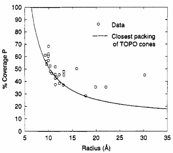
The fit indicates that as the nanocrystal radius increases the amount of TOPO coverage decreases, which is counterintuitive.24
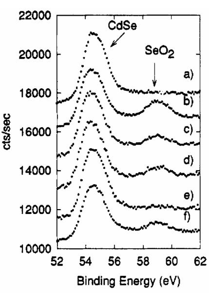
In their study Katari et al. also used XPS to follow the surface oxidation of the nanocrystals. They monitored the Cd and Se peaks as the monolayers were left out in air.24 All samples developed an oxidized Se peak after 24 hours in air while there was no observation of a Cd oxidation peak. The P remained unchanged as well. The Se oxide peak grows in, then decays, and then grows in again (Figure 18). The Cd:Se ratio rises simultaneously with the oxide peak decay, indicating that Se is lost from the nanocrystal. As the surface Cd atoms are bound to TOPO, Bowen Katari et al.24 concluded that the formation of a compound oxide is unlikely and that the oxide formed is SeO2. Finally, XPS spectra for nanocrystals deposited from pyridine solution show a lack of both a phosphorus and a nitrogen peak, indicating that the pyridine displaces the phosphorus and then is pumped off while under vacuum at room temperature, leaving a bare nanocrystal surface.
Figure 18. Dynamics of the growth of a surface oxide on the nanocrystal as monitored by XPS.
This plot indicates the formation of volatile SeO2 which leaves the surface and allows the generation of more SeO2.24
XPS has also been used to verify shelling when making core/shell nanocrystals. Hines et al. observed Zn in the XPS spectrum of CdSe/ZnS core shells.65 Their results indicate three times as much Zn than Cd, to which they attributed the short (50 Å) probe depth. Daboussi et al. took the application of XPS to the studies of core/shells further by studying the degree of passivation of the CdSe surface with ZnS by exposing the nanocrystal surface to air and studying the evolution of the Se peak.67 Their results show that at ~1.3 monolayers of ZnS the oxide peak does not appear, even at long exposure times, suggesting this is sufficient to create a continuous shell of ZnS around the CdSe core. Further, for core/shells with more than 1.3 monolayer coverage, no change in the Cd:Se ratio was observed, even after 80 hours in air, indicating Se did not desorb as an oxide and the shell was complete. Another method to probe the spatial location of the ZnS relative to the CdSe core used by Daboussi et al., was to compare the ratios of the XPS and Auger intensities of the Cd photoelectrons for bare and overcoated samples.67 This analysis confirmed the growth of ZnS on the surface of CdSe cores. Another example of the use of XPS to analyze core/shells is the work of Peng et al., in which CdSe/CdS cores were compared to CdS films.71 These results, combined with the concept of the escape length, were used to analyze the structure of the core/shell. Recognizing that the intensity of the core Se is limited in escape by the shell, according to I/Io=exp(−z/λ), with λ as the escape length, the authors were able to demonstrate that the structure was indeed a core/shell and not an alloy. Such results are critical to understanding the photoemission properties of the semiconductor structure with respect to band-gap and quantum confinement.
The thorough study of Katari et al. demonstrates that it is possible to apply traditional, high vacuum, surface science techniques to the study of nanocrystals.24 The methodology for using hexane dithiol to tether nanocrystals to a gold surface could be extended to other techniques. Nanocrystal composition, surface ligand coverage, surface shell coverage, and surface oxidation have been examined by XPS. A different methodology will be needed to determine surface structure and reconstruction at the atomic level. As we will see below, one technique which might fully achieve this is high resolution Z-STEM.
3. 2 Nuclear Magnetic Resonance Studies of Ligand Surface Coverage
Nuclear magnetic resonance (NMR) can reveal information about crystallite surfaces due to its ability to probe local chemical environments. Becerra et al. applied magic angle spinning, solid state, 31P NMR to the study 37 Å diameter CdSe nanocrystals prepared in TOP/TOPO in order to investigate surface morphology.82 Both TOPO and TOP (bound to Se) were identified in the NMR spectrum with 55% coverage of all surface atoms; 70% of the ligands are TOPO and 30% are TOP:Se. The TOP:Se capping species can be removed by preparing the nanocrystals in 4:1 TOPO:TOP and exchanging the surface TOP with warm TOPO. An average P-P distance of 8 to 10 Å was determined by spin echo experiments, consistent with capping of alternate atomic sites on the surface. The picture that arises from the NMR study is that the two capping species, TOPO and TOP:Se form a close packed shell which physically stabilizes the nanocrystal and electronically passivates the surface. Unlike the XPS study, it was concluded that all Cd sites are passivated while Se sites are bare. Thermal gravimetric analysis, in conjunction with quantitative 1H NMR, indicated these same 37 Å nanocrystals have only 30% of the surface Cd atoms passivated with either TOPO or TOP bonded to Se.83 One might conclude that while NMR can identify the presence of surface species, it may not be the best tool for quantifying surface species.
3.3 Positron Spectroscopy
One of the more novel surface probes applied to nanocrystals involves the use of positron annihilation.84 In this technique, low energy positrons (~3 KeV) are implanted into a solid, lose their energy, thermalize coming to near rest, and eventually annihilate with electrons of the solid into two ~511 KeV gamma rays. High resolution measurements of the energy distribution of the gammas and their angular correlation, measured in coincidence with two detectors, give information on the momentum distribution of the annihilating electrons. (For a general review of the positron technique see Refs 11, 12, 17 of Eijt et al.)84 These momenta may then be correlated with the band structure and/or used to identify core levels of the annihilating electrons.
In the Eijt et al. experiments, relatively thick films of CdSe nanocrystals were used (~2 μm).84 The shape of the energy distribution sharpens relative to bulk CdSe, indicating annihilation with low momenta electrons. Generally such a sharpening is attributed to positron annihilation with vacancy type defects or at surfaces/interfaces, where the positron is far from the high momenta core. In this case the authors conclude that the positron annihilation is primarily at the surface, as the vacancy concentration would be unreasonably high. Interestingly, the annihilation appears to be independent of the nature of the passivating ligand; the positron wave function is strongest at the interface of the inorganic nanocrystal and the organic ligand.
Finally, the complete analysis suggests that this interface is Se rich, in apparent contradiction with RBS results described here. However the authors point out that “positrons are strongly attracted to the relaxed outer shell of Se”, which gives rise to a preferential sensitivity and may explain the difference. This use of positrons is an additional example of the use of novel probes to address the surface interface problem for nanocrystals. Clearly more systematic studies are required. Nevertheless, it is an interesting example of exploring surfaces in non-planar structures, making use of the fact that the positron seeks the surface site.
3.4 Perspective on Surface Analysis and Surface Analysis Probes of Nanocrystals
The discussion of surface analysis of quantum dot nanostructures demonstrates the challenges in clear and unambiguous analysis of the surface and interface chemistry and structure. Planar surfaces have been the focus of the surface science community for decades and the probes, both chemical and structural, have need designed for the planar geometry. Standard techniques such as Auger spectroscopy, x-ray photoelectron spectroscopy, surface sensitive ion scattering all possess characteristics that do not lend themselves straightforwardly to the quantum dot geometry. For example, the fact that the escape length in conventional XPS is comparable to the size of the nanocrystals makes definitive surface analysis difficult. It is clear that more atomic level probes need to be applied to the problem. The clearest example would be the use of scanning tunneling microscopy investigations, although interfacial chemistry will still be problematic. While advances have been made in the surface analysis of nanocrystals, this pursuit remains the most challenging aspect in quantum dot characterization.
4 Rutherford Backscattering of CdSe and CdSe/ZnS Nanocrystals
Rutherford backscattering is a well known tool in surface science.42 With its high sensitivity of detection and ability to provide extremely accurate elemental composition it is an ideal tool for determining the composition of core and core/shell nanocrystals. We have made extensive use of RBS to analyze the composition of nanocrystals. In this section we begin with a discussion of the theory of RBS.41, 58, 74, 85 This is followed by a description of how RBS analysis of nanocrystals is performed. Finally, the results of different RBS experiments performed on nanocrystals are presented in section 4.3.
4.1 Theory of Rutherford Backscattering
Rutherford Backscattering Spectroscopy (RBS) can be used to quantify the chemical composition of a sample to an accuracy of better than a picomol.86 RBS consists of a high energy ion beam that is directed at a sample. The basic signal is the ions that are scattered back through large angles, close to 180°. The intensity of backscattered ions is related to the atomic number (Z) of the detected element and the sample thickness. The energy distribution of backscattered ions is used to form a spectrum with the position of the signal along the x-axis dependent on the energy of the backscattered ion while the area of each peak is related to the abundance of the element being detected. With the use of a standard, such as bismuth-implanted Si, the areal density Nt (atoms/cm2) of any element in the sample can be determined.42
| (4.1) |
In Equation 4.1, Yx is the area of the peak for element x. The integrated charge, Qx, is the amount of current collected during sample acquisition. σx is the non-Rutherford correction factor and is determined by Equation 4.2, where Z1 is the atomic number of the detected element and Z2 is the atomic number of the gas used to create the ion beam divided by Elab, the beam energy in KeV.
| (4.2) |
The absolute accuracy in determining the number of atoms per cm2 using the Bi standard is ~ 5 %.
4.2 Performing RBS experiments on nanocrystals
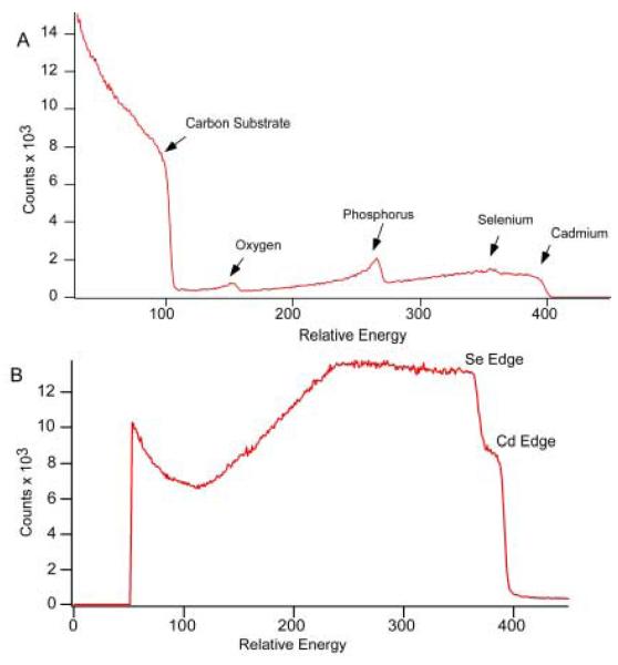
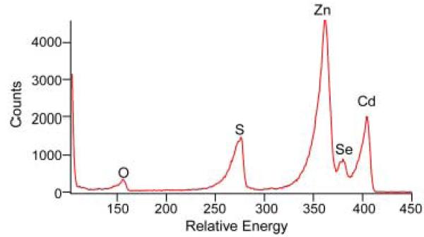
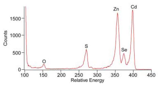
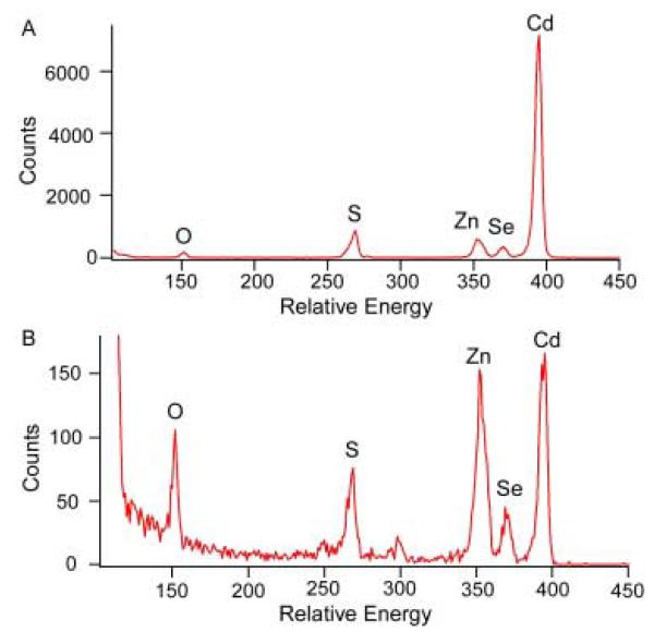
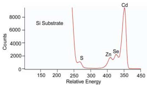
RBS samples were prepared by washing the nanocrystals to remove excess surfactants and organometallic precursors. Excess surfactants can leave an insulating coating on the graphite substrate that causes peak broadening, while excess starting materials cause the experimentally determined atomic ratios to be non-representative of the nanocrystals in the sample. Once the samples were washed, a solution of nanocrystals with an optical density greater than 0.3 was made using a volatile solvent such as toluene or chloroform. Next, one or two drops were placed onto a piece of pyrolytic graphite (Carbone of America) that had been cut to roughly 1 cm2 in size. Once the entire piece of graphite was coated, the solvent was then wicked off by touching the corner of the graphite with a Kimwipe™. This action drew the solvent off the graphite, leaving a uniform coating of nanocrystals without the formation of drying marks. Pieces of a silicon wafer were also used in the same fashion if a smoother surface was required and information for elements lighter than the silicon edge was not needed. If there were excess starting materials, or the sample was too thick, the spectrum could be difficult to decipher (Figure 19).87
Figure 19. Poor RBS spectra.
The spectrum in Figure 19A is the result of large amounts of insulating organic reagents and rough surfaces leading to peak broadening. The spectrum in Figure 19B is the result of the sample being too thick as the clear onset of the substrate is obscured by the sample. Both spectra illustrate the necessity of clean nanocrystals and good sample preparation to obtain information from RBS.87
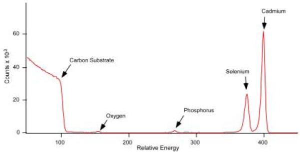
The Van de Graaf generator was typically set to run at 1.8 MeV with He as the ion source and a 1 mm aperture in-line with the beam. The samples were attached to a multi-sample holder using either a small piece of conductive carbon tape or by using copper clips. Each day, a spectrum of a bismuth standard with a known areal density of 4.77 × 10¹⁵ atoms/cm2 was acquired before data collection to ensure that the detector was functioning properly and to facilitate normalization for quantitative studies. Currents of around 10 nA on the Faraday cup, which measures the current carried by the ion beam, were adequate for characterization of thin films or nanocrystal samples. Using too high a current would lead to increased dead time. The detector was run under a 50 V bias and all data was collected through a program written in Igor Pro.88 An example of a good RBS spectrum of CdSe is shown in Figure 20.
Figure 20. RBS spectrum of CdSe nanocrystals.
This is a typical RBS spectrum of a CdSe nanocrystal sample on a graphite substrate. The peaks appear in order of atomic number with the lighter elements appearing at lower channel numbers. The substrate appears as an ‘edge’ due to its thickness.
An RBS spectrum is a plot of the number of counts per channel number. The heavy Cd and Se atoms appear at the highest energy in the spectrum, while lighter elements such as oxygen appear at lower energy (channel numbers). The substrate appears as a step edge followed by a sloping continuum of counts. This is because of the loss of scattering energy and increased cross-section as the beam penetrates deeper into the substrate. Individual peaks were assigned to specific elements by fitting the channel numbers to a line equation using tabulated kinematic factors. Once the elements are identified, the areal densities in atoms/cm2 for each element are calculated. Although traditional elemental analysis can also provide similar results, the availability of the accelerator facility on site and the increased accuracy makes RBS the better choice for nanocrystal studies.
4.3 RBS Results for Different Nanocrystal Systems
RBS data not only provides elemental composition of nanocrystals but also lends insight in to the structure of the nanocrystal. In this section we provide four examples of the use of RBS to provide insight into the nature of CdSe nanocrystals
4.3.1 RBS determination of non-stoichiometric TOPO capped CdSe nanocrystals
As described above in Section 2, for many years the most popular method for synthesizing nanocrystals was the TOPO only method, without addition of co-surfactants. Our initial exploration into implementing RBS to investigate nanocrystal composition was performed on these TOPO only prepared nanocrystals.74 Not only did it immediately become apparent that RBS was a powerful tool for determining nanocrystal stoichiometry, but information on surface ligand coverage and insight into nanocrystal structure could also be obtained. We determined that these nanocrystals are non-stiochiometric, with a Cd:Se ratio of 1.2:1 ± 0.1, that all surface Cd atoms are passivated by TOPO, and that the ideal location of the excess Cd was at the Se-rich (010′) facets (Figure 8). We did not observe channeling of the He ions through the nanocrystal due to the random orientation of the nanocrystals on the substrate.
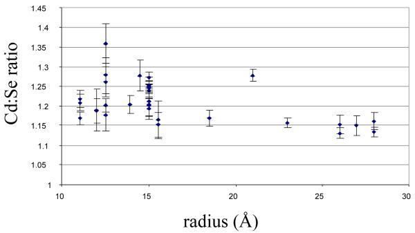
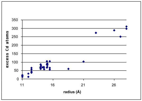
The absolute Cd:Se ratios determined for nanocrystals ranging from 22 Å to 56 Å in mean diameter are summarized in Figure 21. In all cases we found the nanocrystals are Cd rich. The Cd:Se stoichiometry decreases from 1.2 at 22 Å to 1.15 at 56 Å. To convert the Cd:Se ratios in Figure 21 to a number of excess Cd atoms (Figure 22) it is only necessary to know the total number of atoms in a nanocrystal of a given mean diameter, which is the atomic density of CdSe multiplied by the volume of the nanocrystal. Using the experimentally determined shape and size dependent aspect ratio (long/short axis, Section 2.4 above), we determined the volume of a hexagonal prism capped with two frustums to obtain the volume of the nanocrystals and thus the number of Cd atoms.
Figure 21. Stoiciometry of TOPO-prepared CdSe nanocrystals determined by RBS.
The average Cd:Se ratio of all samples is 1.2:1 ± 0.1, indicating that the nanocrystals are Cd rich.74
Figure 22. Number of excess Cd atoms on TOPO prepared CdSe nanocrystals as a function of size.
The change in the stoichiometry due to size is likely the result of asymmetric growth as the nanocrystal becomes larger.74
The size dependence of the excess Cd atoms depicted in Figure 22 does not follow a simple r2 dependence. Given the non-spherical shape of the nanocrystal and the non-uniform surface sites for excess Cd, discussed below, this is to be expected. The characterization of these nanocrystals by X-ray diffraction indicates the core is stoichiometric wurtzite. The luminescence is dominated by the band edge fluorescence, indicating the absence of vacancy defects which would have to be present if the excess Cd were distributed throughout the crystal. We therefore conclude the excess Cd is on the surface of the crystal.
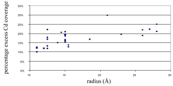
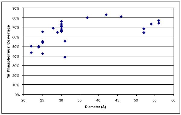
In Figure 23 the excess Cd is displayed as a fraction of the total surface atoms. The total number of surface atoms is obtained by calculating the total surface area and multiplying by the atomic surface density. Values of the excess Cd coverage are in the range of 15-20%, consistent with a substantial surface enrichment. These values indicate that approximately 1 in every 5-6 surface atoms is an excess Cd atom. The absolute P:Cd ratios determined by RBS are extremely similar to those determined by XPS.24 The percentage of phosphorous atoms covering the surface atoms as determined by RBS is presented in Figure 24.
Figure 23.
Excess Cd atoms in TOPO-prepared CdSe as a function of size given as a percentage of total atoms.74
Figure 24. Surface coverage of TOPO on CdSe nanocrystals as a function of nanocrystals size as determined by RBS.
This data contradicts the XPS results, instead suggesting slight increase of coverage as the nanocrystal size increases. This is likely due to the steric bulk of the TOPO ligands limiting the maximum amount of coverage of small nanocrystals.74
As XPS analysis indicated that there was no tributylphosphine coordinated to the nanocrystals, each phosphorous atom represents one TOPO molecule. From this data we obtain an average TOPO surface coverage of 70 %. This TOPO surface coverage is larger than that reported by XPS. This difference originates from considering the atomic surface density of a hexagonal prism capped with two frustums and counting only those atoms which are not fully four-fold coordinated as surface atoms.
The RBS analysis reveals intriguing insight in to the structure of these TOPO only nanocrystals. The presence of excess Cd is not due to contamination from unreacted starting material as RBS analysis of the supernatants used in the washing procedure verified that unreacted Cd and Se are completely removed with the third methanol wash. The excess Cd is either a result of the initial excess Cd used in the synthetic reaction mixture or is a result of the surface passivating ability of the TOPO ligand. We found the stoichiometry to be independent of the initial amount of Cd in the reaction mixture, therefore the excess Cd must be due to the stabilization of Cd dangling bonds by the passivating TOPO.
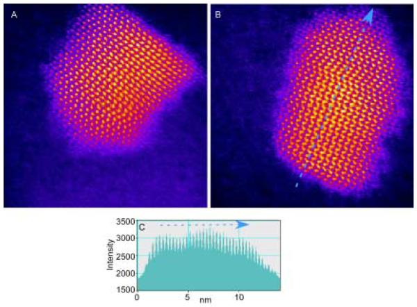
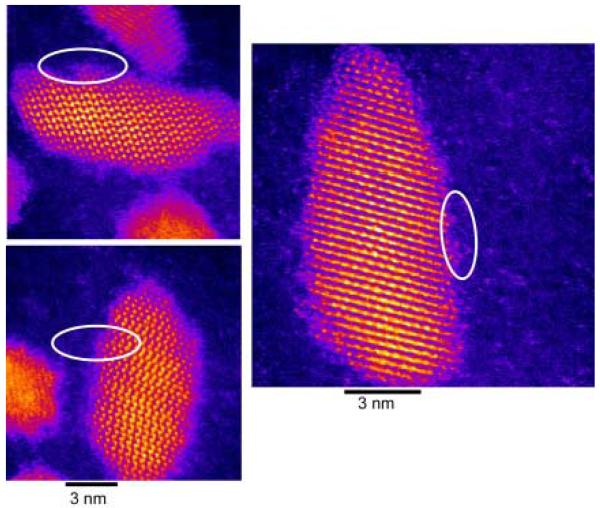
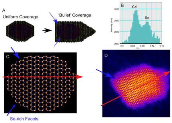
Dangling bonds from unpassivated Cd and Se surface atoms lead to higher energy surfaces. As described above in Section 3, XPS indicates surface Se atoms are bare while surface Cd atoms are coordinated to TOPO. It is therefore consistent that excess Cd would passivate surface Se atoms. However, not all surface Se atoms are equivalent. For example, Se atoms on the (101) facets (see Figure 8) are ideal sites for excess Cd, as one Cd atom can tie up two Se dangling bonds without the addition of strain energy or requiring surface reconstruction. The Se atoms on the top surface Se (001′) and equatorial CdSe (100) planes, however, have only one dangling bond. If excess Cd atoms passivated these Se surface atoms, one dangling Se bond would be passivated but two Cd dangling bonds would be created, so this is a less favorable site for excess Cd. Preferential passivation of the Se facets is also consistent with the observation that CdSe nanocrystals prepared in TOPO have a permanent dipole moment,76 as the Se (001′) terminating plane retains its partial negative charge. Location of excess Cd atoms at the Se facets would lead to an egg shape of the nanocrystals. This shape can be seen in some Z-STEM images of large nanocrystals (below in Section 5, Figure 45). The passivation of Se atoms with two dangling bonds also explains why the midgap absorption features predicted by Leung and Whaley are not observed experimentally.23, 89 Thus, the RBS results not only provide insight into nanocrystal structure but helps explain other experimental and theoretical observations.
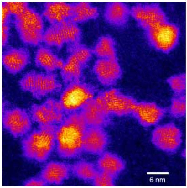
Figure 45. Z-STEM of TOPO CdSe.
This is one of the first aberration corrected Z-STEM images of a CdSe sample. The shapes of the nanocrystals seem irregular with some exhibiting an elongation along the c-axis.
4.3.2 RBS determination of Stoichiometry of TOPO/HDA CdSe Nanocrystals
While nanocrystals synthesized with TOPO alone are Cd rich leading to an egg-like shape, nanocrystals prepared with TOPO/HDA have a symmetrical round shape (Figure 48 in section 5).58 The uniform shape found in the TOPO/HDA sample might be the result of more even growth between the different facets with the addition of HDA to the reaction mixture. This slower growth mechanism allows for surface reconstruction to take place, which is necessary for achieving high fluorescent quantum yields.60 Also, it has been shown that the impurity analogue, in this case dodecylphosphonic acid (DPA), enhances growth along the C-axis, which is an unwanted effect. The addition of HDA seems to prevent this unidirectional growth. The structural differences seen in the nanocrystal images found in Figures 46a and 46b seem to support these two conclusions. The elimination of the elongated (101) facets is also accompanied by the elimination of the excess Cd described above. RBS analysis indicates that the Cd to Se ratio for the TOPO/HDA prepared sample was near unity, supporting the claim above that excess Cd in TOPO only nanocrystals was located on the (101) facets. Figure 25 is a compilation of RBS experiments on three different sizes of HDA/TOPO prepared CdSe. For the CdSe nanocrystal sample with a diameter of 3.2 Å and 4.5 Å, the Cd:Se ratio was around 1.02, much lower than for the nanocrystals formed with TOPO alone as described above. The RBS spectrum for the 35 Å diameter nanocrystals with a Cd to Se ratio of 0.94 has a slight overlap between the Cd and Se peaks, giving rise to additional uncertainty in this case.
Figure 48. Z-STEM of 81% quantum yield Cd-doped CdSe/ZnS core/shell nanocrystals.
Figure 48a is the first lattice resolved image of a graded core/shell nanocrystal. Because of the grading, it is no longer possible to see an abrupt core/shell interface. Figure 48b shows a core/shell nanocrystal associated with a ZnS nanocrystal. The intensity profile in Figure 48c illustrates how the mass contrast in the image can be used to identify dark particles.
Figure 46. Comparison of TOPO CdSe and TOPO/HDA CdSe.
The nanocrystals in Figure 46b are far more spherical in shape than those of the TOPO only nanocrystals, Figure 46a. Figure 46c shows that the (101) face is elongated for the TOPO only nanocrystals. Figure 46d shows a line profile of one of the atomic dumbbells used to identify the Se face.
Figure 25. RBS of TOPO/HDA Nanocrystals.
Three RBS spectra taken of three different sizes of TOPO/HDA prepared CdSe. Each have a Cd:Se ratio lower than what has been previously reported for TOPO only nanocrystals (Figure 21). Unlike the nanocrystals prepared in TOPO only, these do not show a trend of increasing excess Cd as the nanocrystal size increases. This is likely the result that the large nanocrystals are the same shape as the smaller nanocrystals.
4.3.3 RBS of CdSe/ZnS Core Shell Nanocrystals
RBS was used to determine the elemental composition of CdSe/ZnS core/shell nanocrystals prepared using literature methods (Section 2.3). If the majority of the elements detected are from the core/shell nanostructure and if the shell is coating all the surfaces of the core evenly, then it is a simple calculation to determine the shell thickness using the elemental ratios obtained through RBS. For example, if the core radius is known for a CdSe/ZnS core/shell sample, the shell thickness can be determined by using the ratio of Cd to Zn, then using the density of CdSe, back calculating the density, and then the thickness of the shell. The problem with this technique however, is that often the shell does not cover the core uniformly. Additionally, it is very difficult to remove the excess reagents by standard cleaning procedures due to an often complex mixture of surfactants used in the synthesis. Figure 26 shows the RBS spectrum for the CdSe/ZnS core/shell nanocrystal thin film that was provided by Quantum Dot Corp. and was synthesized using literature methods described above in Section 2.3.67
Figure 26. RBS of literature-prepared CdSe/ZnS core/shell nanocrystals.
Peaks indicate the presence of Cd, Se, Zn, and S as expected for a core/shell. The ratio for Zn:Cd was determined to be 8:1. The high Zn content is likely not all from shell material but from ZnS nanocrystals as well that can form during the shell growth. The peak tailing in this spectrum is likely due to the sample being too thick.
The Zn to Cd ratio for this sample was calculated to be nearly 8 to 1. The high Zn content is likely not all from shell material but also from ZnS nanocrystals that can form during shell growth. CdSe and ZnS have an 11 % lattice mismatch, so one strategy to obtain improved shell growth is to dope Cd into the shell, reducing the mismatch. Figure 27 shows the RBS spectrum of the first core/shell nanocrystals where Cd precursor was added during the shelling process. This core/shell sample had a core size around 70 Å and a fluorescence quantum yield of 39%. The extra Cd content can be seen in the RBS data as the reduction of the ratio of Zn to Cd to 3:1. Due to the incorporation of Cd to the shell, the simple assumption that the Cd detected is only from the core no longer holds. To elucidate the true shell shape and composition, RBS must be combined with Z-STEM to determine the shape and elemental composition of core/shell nanocrystals as described below in Section 5.41
Figure 27. RBS of 39% quantum yield Cd-doped CdSe/ZnS core/shells.
The Zn:Cd ratio has been reduced from 8:1 to 3:1 due to the presence of the doped Cd.
Following through with the Cd addition during shell growth, another pair of samples with higher cadmium content in the shell from Quantum Dot Corp was examined. These two samples had core sizes of 3 and 5 nm, and had quantum efficiencies of 81% and 82%, respectively. Figures 28a and 28b show the RBS spectra taken from two core/shell samples with very high quantum yields. From the RBS data it was concluded that the amount of Cd does not necessarily affect the quantum yield since both of these samples had vastly different amounts of Cd in them. These samples had about the same quantum yield yet the 5 nm core/shells had a Cd to Zn ratio of nearly a factor of 10 greater than that of the 3 nm core/shell sample. The ratio of Cd:Se was found to be 8.8:1, which suggests that the increase in Cd is due to the shell and not the change in the size of the CdSe core. A better comparison would be to adjust the amount of Cd introduced into the reaction mixture for two samples with the same core size.
Figure 28. RBS of 81% and 82% quantum yield samples with Cd-doped CdSe/ZnS core/shell nanocrystals.
The amount of Cd is far greater for the 81% quantum yield sample, 28a, compared to that of the 82% quantum yield, 28b. This suggests that the absolute amount of Cd does not directly affect the quantum yield.
The intended use of core/shell nanocrystals is primarily in biological labeling. Water-solubility is crucial for biological studies; however, the extra polymer layer that enables water solubility (see below in Section 6) complicates the problem of quantifying the effectiveness of an inorganic shell. The surface ligands could be more effective at removing surface traps and may be more photostable when encased in this polymer shell. The other experimental drawback to the polymer coating is that a large excess of polymer material is in solution with the core/shell rods, complicating RBS data collection by coating the graphite substrate and causing peak broadening. Figure 29 shows an RBS spectrum of the 655 nm emitting, amphiphilic polymer (AMP) coated dots on Si.
Figure 29. RBS of 655 AMP™ core/shell rods on Si.
A large excess of Cd is seen in this spectrum. The large overlap, however, is due to the excess of AMP found in the sample.
A piece of Si was chosen as the substrate material in order to provide a smoother, more polar, surface which improved the peak separation. The Cd to Zn ratio for this sample was determined to be 2:1. Figure 30 shows the RBS spectra for the 605 AMP quantum dots. Much like the case of the 84% quantum yield sample, the 605 AMP dots have a largely different Cd to Zn ratio compared to the 655 AMP dots, but still maintain a near unity fluorescence quantum yield. The peaks are fairly broad due to the excess of AMP coating the surface. This could also be related to the large amount of phosphorous detected in this sample, which would indicate the sample was not washed well before the polymer coating was applied.
Figure 30. RBS of 605 AMP™ core/shell rods.
As with the 655 AMP sample, poor peak separation is seen due to the large amounts of polymer in these samples. However, this sample has a much larger Cd content.
4.3.4 RBS of alloy nanocrystals
Pseudobinary (II-VI:II-VI) alloy nanocrystals are an intriguing new area of study in nanocrystal research.5, 12, 14, 85, 90-93 They provide an additional degree of freedom in selecting desirable properties for nanoscale engineering, because their physical and optical properties depend on both size and composition. Any study of alloy nanocrystals must include some analysis of alloy composition and homogeneity, for it has been demonstrated that: (a) the proportion of atoms in synthesized nanocrystals is not necessarily the same as the proportion of atoms in the reaction mixture, and (b) alloy nanocrystals may have a gradient structure, in which the composition in one part of the nanocrystal is unlike that in another part of the nanocrystal, thereby changing the properties of the nanocrystal.85, 92
We have recently used RBS to determine the composition and homogeneity of CdSxSe1-x nanocrystals.85 Although RBS can provide a depth profile of composition in thin film structures, most nanocrystals are too small for traditional RBS techniques to distinguish different concentrations at different depths within the nanocrystals. Typically, conventional RBS does not have the resolution to provide a profile of composition as a function of depth in crystals < 10 nm. High resolution RBS techniques however should be adequate for this purpose. The results in our work use conventional RBS.94
To determine whether the alloys were homogeneous or gradient, small aliquots of the nanocrystal solution were removed from the reaction vessel periodically during nanocrystal growth. The aliquots were cleaned, and RBS was performed to determine the composition of the nanocrystals as a function of growth time. A gradient structure is indicated by composition that changes with growth time, while a homogeneous structure is indicated by unchanging composition. Figure 31 shows the RBS-determined composition of alloy nanocrystals, with a precursor sulfur fraction of 0.4, as a function of growth time for nanocrystals grown using three different concentrations of one of the reagents, tributylphosphine (TBP).
Figure 31. Alloy composition as a function of TBP in the reaction mixture.
Alloy composition as a function of growth time for CdS0.4Se0.6 grown using Se precursor solutions that were 2.5% (○), 3.0% (□), and 8.3% (+) TBP by volume. The 8.3% precursor shows a strong increase in sulfur with growth, indicating the formation of gradient alloys. The 3.0% precursor shows a slight increase in sulfur, and the 2.5% precursor a slight decrease. It is noted that the nanocrystals produced using the 2.5% TBP precursor were synthesized with the use of growth solution, unlike the 3.0% and 8.3% nanocrystals; the 2.5% nanocrystals are therefore much larger.85
Analysis shows that of the three different TBP concentrations, a 2.5% TBP precursor produced the most homogeneous alloy, while an 8.3% TBP precursor yielded a strongly gradient structure. In this case, results from RBS prompted a change in synthetic strategy until the desired result was achieved.85 The experiment was repeated for all sulfur fractions (Figure 32), showing that homogeneous CdSxSe1-x could be produced using the same general synthesis simply by varying x in the reaction.
Figure 32. Alloy composition as a function of growth time for CdS0.8Se0.2 (○), CdS0.6Se0.4 (□), CdS0.4Se0.6 (△), and CdS0.2Se0.8 (◇).
RBS analysis of aliquots of nanocrystals pulled from single batches of nanocrystals during growth reveals that the composition of the nanocrystals remains reasonably constant over the growth period, an indication of alloy homogeneity.85
5. Atomic Number Contrast Scanning Transmission Electron Microscopy (Z-STEM) of CdSe and CdSe/ZnS Nanocrystals
Atomic Number Contrast Scanning Transmission Electron Microscopy (Z-STEM) provides an unmatched ability to achieve structural and chemical information from individual nanostructures at the atomic level.44, 95 For example, Z-STEM tomography was recently used to determine the 3 dimensional structure of less than 10 nm Sn quantum dots embedded in Si with cubic nanometer resolution.96 Z-STEM has been used for many years to directly image the atomic structure of grain boundaries and interfaces, even revealing specific impurity segregation sites.97-99 A key advantage of Z-STEM is that it can be easily combined with Electron Energy Loss Spectroscopy (EELS) to achieve elemental identification with atomic resolution.100 Today, with the successful correction of lens aberrations, Z-STEM has demonstrated 0.78 Å spatial resolution by directly imaging Si [112] atomic dumbbells.44 The higher resolution and image contrast also result in a greatly improved sensitivity for EELS, opening many opportunities for materials science research.101 For example, it was shown using these two techniques that rare earth dopant atoms, such as La, preferentially segregate to the amorphous crystal interfaces of Si3N4102. This level of precise information is critical for the development of nanomaterials where the placement of a single atom could drastically affect the desired properties.
We have applied Z-STEM to the study of core and core-shell nanocrystals.41, 43, 58 In this section we first present a description of Z-STEM operation and provide illustrative comparisons between TEM and Z-STEM imaging of nanocrystals. In section 5.2 alternatives in image analysis are discussed, followed by the presentation of experimental results for different nanocrystal systems in Section 5.3.
5.1 Z-STEM Operation
Scanning Transmission Electron Microscopy (STEM) and Atomic Number Contrast STEM (Z-STEM) use a focused electron beam that is rastered across the sample. A typical STEM setup is shown in Figure 33. Like TEM, an electron beam is used to form an image. However, the electron beam is focused to an atom-sized probe that scans across the sample to form an image. The electrons that are scattered at low angles are used to form a bright field image while those scattered at high angles are used to form a dark field image. Also, the nature of the scattering process is different: the bright field image is a coherent phase contrast image, as would be formed in a comparable high-resolution TEM. High angle scattering is generated incoherently, and leads to an incoherent image the resolution of which is directly related to electron probe diameter. The electron probe size is limited only by the beam energy, its energy spread, and by aberrations in probe forming lenses.103 Also, high-angle scattered electrons show a strong atomic number contrast hence the term Z-STEM or Z-contrast imaging, also known as high-angle annular dark field (HAADF) imaging.43, 45, 46 These electrons behave much like the He ions in Rutherford Backscattering in that their energy and intensity is dependent on the material with which they interact. Electrons impinging upon a heavy atom will scatter more frequently to higher angles than those that encounter a lighter atom. Scattered electrons detected from different atoms appear as intensity variations in the image, which yields elemental information directly from the image. Unlike coherent imaging techniques such as phase contrast imaging, there are no complicated contrast changes with focus or specimen thickness.104 This allows for direct interpretation of the images; a bright spot in the image plane corresponds directly to a scattering center in the object plane, i.e. an atom. Additionally, the intensity of the scattered electrons depends on the square of the atomic number of the scattering atom, yielding spatially resolved chemical information.43 The incoherent scattering of the electron is described by the Rutherford scattering formula (Equation 5.1):
| (5.1) |
The left side of the equation denotes different scattering cross-sections as a function of the scattering angle θ. E0 is the incident beam energy, e is the electron charge, and Z is the atomic number of the scattering nucleus. This equation predicts that the intensity of the scattered electrons is dependent on the square of the atomic number (Z2) for a sufficiently high angular range where screening by the electron cloud can be ignored. For this reason, atomic number contrast can be observed directly from the image.
Figure 33. Z-STEM setup.
The electrons are focused into a narrow electron probe that is then scanned across the sample. The electrons that are scattered at high angles are collected by the HAADF detector and used to form the Z-STEM images. Weakly scattered electrons pass through the annular detector and can be used for Electron Energy Loss Spectroscopy (EELS) or for forming a Bright Field (BF) image.
Intensity is also dependent on sample thickness allowing for direct measurement of an object’s three-dimensional structure from the image. A comparison between two comparably orientated CdSe nanocrystals imaged under HRTEM and Z-STEM is shown in Figure 34.
Figure 34. Comparison of Z-STEM and HRTEM.
The phase contrast HRTEM image obtained with 200 kV Phillips TEM, Figure 34a, does not distinguish the Cd and Se columns and shows little intensity difference between the edge of the nanocrystal and the amorphous carbon support making it difficult to assign faces. However, in the Z-STEM image in Figure 34b of a similarly aligned nanocrystal, the intensity is dependent on the atomic number of the material being imaged. Figure 34c shows how the mass contrast between the Cd and Se columns can be used to determine the specific facets seen in the image, Figure 34d.
False color has been added to the Z-STEM image to emphasize the importance of the image intensity. Unlike the conventional HRTEM image in Figure 34a, chemical and structural information can be obtained directly from the intensities in the raw Z-STEM image. For example, the Cd and Se columns in Figure 34b can be assigned from the intensity difference found in the raw image, as indicated by the intensity profile in Figure 34c. With this information, the Cd-rich (001) and the Se-rich (001′) surfaces can be then assigned by following the alternating intensities to the surface, as shown in Figure 34d. Additionally, since the electrons that are detected are incoherently scattered, phase contrast that produces the speckle pattern in bright field images of amorphous carbon is not present. As a result, single atoms can be imaged on the surface of an amorphous carbon film, and nanocrystal edges are clearly visible in cases where the nanocrystal is not susceptible to oxidation.105 In this case the edges are oxidized due to exposure to air, and the amorphous oxide layer, which has been enclosed by a white circle, can be clearly seen in the Z-STEM image in Figure 34d. The spots seen in the oxide are the remains of the outer surface of the nanocrystal. Individual atoms and atomic clusters can readily be found in this region; these atoms and clusters would not be visible using conventional HRTEM since there is no contrast between amorphous materials and the amorphous carbon support.
The primary limits in resolution of Z-STEM are the signal-to-noise ratio due to the sample thickness, and how small the probe can be made.106 A key limiting factor is the inherent aberrations that broaden the electron probe, which are introduced by the electron lens. With the successful development of STEM aberration correctors, the 100 kV and the 300 kV STEM’s at Oak Ridge National Laboratory were fitted with Nion spherical aberration (Cs) correctors, resulting in an improvement in resolution by roughly a factor of two.
The principle of the aberration corrector is similar to that of a stigmator found in conventional TEM instruments, in that it corrects aberrations by introducing compensating magnetic fields into the beam line.103 The required fields are more complex in form than necessary for simple astigmatism, and the Nion corrector is therefore composed of four strong quadropoles, three strong octupoles and 24 multipoles. The problem with this approach is that a Cs corrector also introduces ‘parasitic’ aberrations of its own, limiting its effectiveness. Clearly, it would be impractical to attempt to adjust all of these by hand, so a computer controls the manipulations of the corrector.
Besides the smaller probe size, an additional advantage of aberration correction is that the STEM Bright Field (BF) image has about two orders of magnitude more current, and becomes practically useful additional channel of information. It is obtained simultaneously with the Z-STEM image, and is equivalent to an aberration-corrected HRTEM image by the principle of reciprocity (reversing ray directions). Figure 35 shows the simultaneous BF and Z-STEM images taken after installation of the aberration corrector. The BF image now shows the edge of the nanocrystal more clearly, because of the reduced image delocalization, but it is still not able to detect individual atoms on the amorphous carbon support because of the lack of strong Z-contrast. The Z-STEM image does show individual atoms and small clusters on the carbon film. The line profiles in Figure 35c and 35d illustrate how the bright field image is formed by constructive and destructive interference on top of the contrast from the carbon support, whereas the Z-STEM image exhibits a sharp increase in intensity between the carbon film and the nanocrystal, indicating the precise location of the surface. However, the bright field image is still particularly useful for finding focus and for manually adjusting for astigmatism, although it should be noted that optimum focus for a bright field image is not exactly the same as optimum focus for the Z-STEM image.104
Figure 35. Simultaneous Z-STEM and BF imaging.
Figures 35a and 35b are BF and HAADF images taken simultaneously of a CdSe/CdS core/shell nanocrystal. The line profiles in 35c and 35d illustrates the intensity separation between the background and the nanocrystal is vastly improved for the DF image. This allows for high-resolution imaging of low contrast objects such as a nanocrystal surface, and the imaging of single atoms and small clusters on the carbon support.
Z-STEM of CdSe Nanocrystals
In this section we illustrate the power of Z-STEM to extract nanocrystal morphology and structure. After a brief description of experimental protocol we demonstrate how Z-STEM provides “one-shot imaging” to obtain the nanocrystal’s three dimensional shape. In section 5.3.3 we present the results of interrogating nanocrystal morphology for two of the synthetic routes described above in section 2. Z-STEM results indicating the structure of unity quantum yield core/shell nanocrystals are then presented. The section concludes with preliminary Z-STEM investigations into the structure of magic sized nanocrystals.
5.3.1 Z-STEM Experimental
Samples for Z-STEM were made up of a very dilute solution of thoroughly washed nanocrystals in toluene. It is extremely important to have the sample completely free of excess surfactants and starting organometallics. Typically, nanocrystals are synthesized in a surfactant such as TOPO or HDA that allows them to be processable. Under conventional TEM conditions, large amounts of this material will cause a noticeable loss in image resolution, contrast, and will cause the TEM grid to charge and contaminate. Contamination is the term used to describe the pileup of organics under the electron beam. The organics, presumably polymerized hydrocarbons, can eventually become so thick that the sample can become opaque to the electron beam. In the case of STEM, the highly focused electron beam exacerbates this problem so that even the most pristine samples contaminate to some extent. To check sample viability prior to insertion into the STEM, the sample can be placed into a conventional TEM and illuminate a single spot on the sample at maximum magnification for a few minutes. If no contamination is observed the sample will be suitable for imaging in a STEM. To make the sample, a drop of the clean nanocrystal solution was allowed to dry on ultra-thin carbon on lacey support TEM grids purchased from Ted Pella, Inc. This was usually done the day before imaging and stored in a TEM grid box overnight.
5.3.2 “One Shot” Determination of the 3 Dimensional Nanocrystal Shape
The following figures show how easily the images can be interpreted. There are three main orientations that allow lattice-resolved images. Examples of these are shown in Figure 36. The images can be modeled by using a computer generated ‘ball-and-stick’ CdSe nanocrystal model and rotating it in 3-D. This particular model was developed by Andreas Kadavanich using Crystal Maker.107 It is interesting to note that in the image of the nanocrystal in the (100) orientation, Figure 36a, the Cd and Se columns are nearly resolved. The spacing between these two atoms in this orientation is 0.67 Å. The nanocrystal in 36b is in the [001] orientation, showing no mass contrast as the Se and Cd atomic columns are overlapped. In contrast, the nanocrystal in Figure 37a is in the [010] orientation where the Cd and Se atomic columns are separated showing mass contrast. Also, a new orientation that had not been resolved prior to use of the aberration corrector is seen in Figure 37b; it is the [111] orientation with a column separation of 2.75 Å.
Figure 36. CdSe Orientations.
Like TEM, the patterns seen in the Z-STEM images can be related to a CdSe model in the same orientation. The intensity seen in the Z-STEM images is directly related to the nanocrystal’s atomic structure. This allows for a simple comparison between the Z-STEM image and a nanocrystal model to identify the observed orientation. Figure 36a and 36b are high-resolution images of CdSe in the [100] and [001] orientations.
Figure 37. CdSe Orientations.
The nanocrystal in A is in the [010] direction which beautifully illustrates how mass contrast can be used to identify the chemical structure of a nanocrystal at the atomic level. In this orientation the Cd and Se columns are separated. The nanocrystal in B is in the [111] direction.
Since the image intensity is dependent on the amount of material under the beam, the nanocrystal’s 3-dimensional shape can be extrapolated.43 Figure 38a shows a model Z-STEM image of a CdSe nanocrystal. An intensity map is then generated, Figure 38b, which is used to plot the thickness change from the center of the nanocrystal to the surface, Figure 38c and 38d.43 The experimental results in Figure 39 exhibit a shape similar to the model, but image, noise, and intensity differences due to stacking faults in the image prevent a closer match.
Figure 38. Model intensity map.
Figure 38a is a simulated Z-STEM image of a CdSe nanocrystal obtained simply by convoluting the free space probe intensity profile with the projected number of atoms weighted by Z2, a reasonable approximation for small nanocrystals. The intensities can be projected into directions in the plane of the image to obtain a 3-D shape of the nanocrystal, Figures 38c and 38d.43
Figure 39. Experimental Intensity Map.
The intensities from the reconstructed image were used to form an intensity map. Although the overall trend of the intensities seems to match the model, stacking faults in the nanocrystal can be seen affecting the intensity in the image.
The nanocrystal shown in Figure 40a shows a relatively symmetrical intensity along its C-axis as would be expected for a traditional nanocrystal. The 3D cartoon (Figure 40b) is helpful for visualizing the 3D shape of the nanocrystal. However, the nanocrystal in Figure 40c clearly shows a large decrease in intensity for half of the nanocrystal, giving the impression that it is only partially completed or that a possible defect formation prevented further growth. An artist’s conception of the approximate 3-D shape is shown in Figure 40d. From the 3-D shape, it appears that the growth occurs in a stepwise manner, starting at a surface edge and then moving across while building upward along the C-axis. This likely occurs due to the higher number of dangling bonds on the edges of the nanocrystal. With the surface clearly visible in these images, it should be feasible to observe the structural effects of nanocrystal surfactants as illustrated in the following section.
Figure 40. Z-STEM of an Incomplete Nanocrystal.
Figure 40a shows a typical CdSe preparation using the TOPO only method. The mass contrast in the image can be used to form an approximate 3-D shape as seen in Figure 40b. In this orientation, the thickest part of the nanocrystal should be along the middle and should gradually thin towards the edges. The nanocrystal in Figure 40c does not show this trend Instead, it appears to have a large gap in the upper half of the nanocrystal. This is likely an incomplete nanocrystal. The approximate 3-D shape of this incomplete nanocrystal is shown in Figure 40d. Assuming this is an incomplete nanocrystal, the growth mechanism can be determined from the nanocrystal image.
5.3.3 Effect of surfactant on nanocrystal morphology
It has been reported previously that CdSe nanocrystals prepared by the TOPO-only method are Cd rich.74 It is believed that the excess Cd found in the TOPO-only nanocrystals resides in the elongated (101) facets, where there are two Se dangling bonds at each Se surface site. The images indicate that the (101) faces are predominantly favored over the (100) faces, which is likely the reason for the non-stoichiometry found in the RBS experiments (Section 4.3.1 above).74
In contrast, the nanocrystals prepared by the TOPO/HDA method are extremely uniform in size and shape. The nanocrystals seem to be truncated evenly on either side, suggesting a lack of preferential growth or a more controlled growth than that seen in the TOPO-only sample. Since a majority of the nanocrystals are of the same size and shape, spontaneous hexagonal 2D-arrays form exhibiting the same hexagonal structure as the nanocrystals.
Figures 41 and 42 show images of CdSe nanocrystals from the TOPO/HDA sample in the (100) and (001) orientation, respectively. Although there is an oxide layer coating the surface, it is sufficiently thin in some areas to allow the actual surface of the nanocrystal to be seen.43 This was achieved by minimizing the nanocrystal sample’s exposure to air. Unfortunately, difficulties with achieving the correct sample height forced the repeated removal of the sample and subsequent exposure to air. Nevertheless, the amount of oxide on the nanocrystals appeared much less than that of nanocrystals that were evaporated onto a grid the night before and stored under ambient conditions.
Figure 41. High Resolution Z-STEM of TOPO/HDA CdSe Nanocrystals.
Figure 41a shows an aberration-corrected Z-STEM image of a group of CdSe nanocrystals. Figure 41b shows a close-up view of the [010]-oriented nanocrystal. A very thin oxide layer can be seen on the surface and seems to be thicker on the side, (100) surfaces. The atomic spacing between the Cd and Se columns is 1.5 Angstroms in this orientation.
Figure 42. High Resolution Z-STEM of TOPO/HDA CdSe.
Figure 42a shows a rare image of a CdSe nanocrystal in the [001] orientation. This nanocrystal has been enlarged in Figure 42b. Like the nanocrystal in Figure 41, an oxide layer can be seen on the surface. The spacing between the atomic columns is 2.66 Å in this orientation.
Figure 43 shows two Z-STEM images of the TOPO/HDA nanocrystals with a zinc blende crystal structure. These nanocrystals do not exhibit the alternating ‘zigzag’ pattern of a wurtzite nanocrystal. Also, these images exhibit a larger coating of the oxide layer, since this sample was exposed to air for at least 24 hours. Figure 43a is a CdSe nanocrystal in the (010) orientation. This position shows the clearest mass contrast between the Cd and Se columns. However, a crystallographic defect can be seen in the image as there is an extra intensity source in between the atomic columns, probably indicating a stacking fault or twin boundary in the nanocrystal. The nanocrystal in Figure 43b is also in the [010] orientation, but has a stacking fault parallel to the beam direction, indicated by the black line. Twinning of nanocrystals and zinc blende stacking faults are common to CdSe nanocrystals.75 In the case of the nanocrystal in 43b, two zinc blende phases are separated by a wurtzite stacking fault, forming a twin boundary. These low energy defects in the crystal lattice are common for semiconducting nanocrystal systems.78, 108, 109
Figure 43. Z-STEM of TOPO/HDA CdSe with Defects.
Figure 43a shows a zinc blende CdSe nanocrystal viewed along [010]. The black arrow indicates a stray peak due probably caused by a stacking fault or twin boundary with in the nanocrystal. Figure 43b shows a nanocrystal with two zinc blende phases separated by a twin boundary indicated by the black line.
The nanocrystal in Figure 44a shows the typical [001] pattern, but with faint ‘spots’ situated directly in the center of the hexagons. The intensity profile in Figure 44b shows that these peaks are above the noise level in the image and appear perfectly spaced between the other atomic columns. This particular pattern is the result of a stacking fault midway through the nanocrystal that causes a shift of half of the nanocrystal. Figures 44c and 44d show a model CdSe nanocrystal with a similar stacking fault from the [001] and [010] orientations, respectively. The yellow arrow indicates the direction of the stacking fault.
Figure 44. Z-STEM image of a stacking fault in the (001) lattice plane.
Figure 44a is a Z-STEM image of a CdSe nanocrystal in the [001] orientation with an extra set of spots in between the atomic columns. The line profile in 44b shows that the peak intensities are well above the noise level. Figure 44c and 44d shows a model of this stacking fault from the [001] and [100] directions. The crystal lattice has shifted (yellow portion) in the (001) plane creating an ‘extra’ set of peaks in the image.
The Z-STEM data reported above suggests that the addition of HDA to the reaction mixture not only narrowed the size distribution, but also greatly reduced the quantity of shape anomalies compared to the traditional TOPO method. Additionally, Z-STEM provides supporting evidence for the location of the excess Cd in TOPO prepared CdSe nanocrystals and the specific growth face of CdSe nanocrystals. The addition of HDA reduced the size of the (101) facets, which have a high number of dangling bonds, that can act as trap sites for holes. The images in Figure 45 are the first high-resolution images of CdSe nanocrystals obtained shortly after the installation of the spherical aberration (Cs) corrector. The optimum probe size just after installation was around 0.8 Å, demonstrated with the direct imaging of the 0.78 Å spacing in a Si [112] foil.44 The sample from which Figure 45 was collected was prepared by simply placing a drop of nanocrystals in hexanes onto an ultra-thin carbon support grid. The striking detail of the surface of the nanocrystals clearly shows the precise shape of the nanocrystals. Several of the nanocrystals appear elongated, while most exhibit an ovoid shape. The Z-STEM images clearly show a lack of shape distribution control. It was proposed that this might be the result of a ‘magic’ impurity that exists in technical grade TOPO causing an increase in growth along the C-axis.41 CdSe nanocrystals with a good size distribution cannot be grown without this ‘magic’ impurity. However, too much of this impurity leads to uncontrolled growth. It was determined by Peng et al. that the magic ingredient was a phosphonic acid impurity in the TOPO that was necessary to control the shape and growth of the nanocrystals.63 In addition to the phosphonic acid, a long-chain, primary amine, such as hexadecylamine (HDA), was also added to obtain superb size distribution without the need for size selective precipitation.72 It was decided that it would be interesting to determine what difference, if any, the new synthetic scheme had on the characteristics of the resultant nanocrystals. Z-STEM and RBS were used to compare the shape and elemental composition of the nanocrystals made with the new surfactants.58
A comparison between the Z-STEM images of the TOPO- and the HDA/TOPO-prepared nanocrystals is shown in Figure 46. In both images, the large number of lattice-resolved nanocrystals illustrates the benefit of the Cs corrector and the small probe size. Since the nanocrystals are free to rotate, obtaining a good lattice-resolved image is dependent on the orientation of the nanocrystal during image capture. As the probe size decreases, the number of lattice resolved nanocrystals increases due to improved ability to image nanocrystals off axis, and the higher number of zone-axis orientations that are resolvable. The small features seen near the surface would be very difficult to detect using traditional HRTEM.
Interestingly, a striking difference between the two images can be seen. Although the sizes of the nanocrystal samples differ only by 0.3 nm on average, their overall shape is markedly different. The TOPO-prepared CdSe nanocrystals in Figure 46a appear to be elongated, with some exhibiting an ovoid shape, compared to those of the HDA/TOPO-prepared nanocrystals in Figure 46b. For example, the nanocrystal circled in Figure 46a shows a definite narrowing along the c-axis, which is parallel to the surface plane. The inhomogeneous faceting of this sample is likely the result of preferential growth along this axis. From this image, the orientation of the Cd and Se dumbbells can be determined as illustrated by the line profile in Figure 46d, allowing us to assign the narrow end of the nanocrystal as the Se rich (001′) face. This directly assigns the Se rich face as the primary growth face and allows the direct determination of the remaining faces as shown in Figure 46c. The growth direction and growth mode can be seen with more detail in the Z-STEM image in Figure 40, which compares the intensity of a complete nanocrystal compared to that of an “incomplete” nanocrystal.
5.3.4 Characterization of the Shell Structure of CdSe-Based Core/Shell Nanocrystals
Unlike traditional HRTEM that uses phase contrast imaging to gain insight into the crystalline nature of particles, the intensity seen in Z-STEM images depends on the scattering power of the atom being imaged, yielding chemical information simultaneously with structural position. The combination of these two properties makes Z-STEM an ideal tool for studying core/shell structures at the atomic level. The mass difference between the core and shell material manifests itself as a clear change in intensity in the raw images. Coreless, or “dark”, particles are easily identified in the same manner. We chose to study CdSe-based cores/shell systems since they have been previously characterized extensively. The purpose of the shell material is to passivate surface trap sites and to energetically confine the electron and hole. Ideally, for every photon that creates an electron and hole pair, one photon is emitted. To ensure radiative electron and hole recombination, a material with a wider band gap than the core is used to coat the surface. In the case of CdSe, ZnS is typically used as the shell material due to its wide band gap. This is an ideal first system for Z-STEM because of the large mass difference between the ZnS shell and the CdSe core.
Figure 47a shows the first Z-STEM image of a CdSe/ZnS core/shell nanocrystal, prepared using the standard literature preparation by Quantum Dot Corp. with a core size of 3.0 nm and a measured fluorescence quantum yield of 34%.70 The nanocrystal in the center of the raw Z-STEM image features a bright core, with a fainter shell encircling it. Lattice fringes seen on the shell indicate that it is crystalline; however, the shell is not spherical in shape and coats the core unevenly. From this image the existence of coreless particles, presumably ZnS nanocrystals that nucleated during shell growth, is confirmed. These dark particles can be clearly identified by their uniform intensity across the particle. Additionally, a large amount of excess starting material is seen associated with the core/shell nanocrystals appearing as large areas of amorphous material, which is surprising to find after several washings. Finally, an amorphous or semicrystalline shell can be seen on the outermost surface of the core/shells, which is most likely an oxide coating on the ZnS shell.
Figure 47. Z-STEM of Literature Prepared CdSe/ZnS Core/Shell Nanocrystals.
Figure 47a is the first Z-STEM image of a core/shell nanocrystal showing mass contrast between the core and shell. The interface between the core and shell has been marked with a black arrow. Figure 47b shows a core with shell growing from only one facet. The intensity profile in Figure 47c shows the relatively sharp interface between the core material and the shell.
Figure 47b shows an extreme case where the ZnS shell only grew in one direction. This is a direct result of the 11% lattice mismatch between CdSe and ZnS.110 The Se rich, (001′) face of CdSe is typically the most reactive and therefore it is the most likely place for shell growth to initiate. It is likely that this surface remains the most chemically reactive since it has the fewest ligands occupying the surface sites. This leads to a competitive growth process that often leaves the remainder of the core with little or no shell coverage, as with the core/shell shown in Figure 47b. Figure 47c shows a line profile along the C-axis of the core/shell in Figure 47b, illustrating the intensity change going from shell to core due to the mass difference between the CdSe core and the ZnS shell. The interface between core and shell has been marked with a black arrow. The shell can be seen only covering one surface of the core. The large number of ZnS particles found in the sample prepared using the standard literature preparation is likely due to the extreme excess of ZnS precursors that were used in an attempt to force the shell to grow on all the surfaces.
The problem of growing a lattice-mismatched material onto a surface has been addressed before.111-113 When a material is grown onto another material with different lattice spacing, strain energy is created as the chemical bonds are bent and stretched. For a cubic system the strain energy areal density, Eε, can be defined by Equation 5.6.110
| (5.6) |
ε is defined as the in-plane strain, B is the bulk modulus for a thin film (for bulk CdSe, B is 5.5 × 10¹¹ dyn/cm2 at room temperature), and lastly, h is the film thickness. This thickness dependence leads to an important parameter called the ‘critical thickness’ or hc. In equilibrium there is a maximum thickness of material that can be grown on a lattice-mismatched substrate before a dislocation forms. For growth on (100) cubic substrates, hc is defined by equation 5.7.110
| (5.7) |
In this equation, b is the Burgers vector, or the lattice constant of the defect, v is Poisson’s ratio, f is the lattice mismatch, Θ is the angle between the dislocation and its Burgers vector, and λ is the angle between the slip direction the direction that the defect propagates and a line in the interface plane.110 The important result of this relationship is that the critical thickness is inversely related to the lattice mismatch between the materials. Since the lattice mismatch between ZnS and CdSe is nearly 12%, hc is less than 1 nm, so only a very thin ZnS shell can be grown before dislocations form. These dislocations could act as potential recombination centers, degrading the effectiveness of the shell. In order to obtain thicker shells, a shell material that has less of a lattice mismatch with CdSe can be grown initially, followed by a thin coating of the large ‘f’ material. Two potential intermediate shell materials for the CdSe/ZnS core/shell system are CdS and ZnSe, which have lattice constants that reside between those of CdSe and ZnS.
Quantum Dot Corp chose to introduce Cd in the shelling process in order to ‘dope’ the shell to improve shell coverage. This method could produce either a Zn(1-x)CdxS shell or a CdSe/CdS/ZnS double-shelled nanocrystal. RBS analysis was used to confirm the addition of Cd to the shell, with an atomic ratio of Zn to Cd of 3:1 (Section 4.3.3), reduced from the 8:1 ratio found in the literature prepared sample. This indicates that the majority of the shell contains Cd. Although the images obtained do not clearly indicate an outer ZnS shell, due to the varied reactivities of the cation precursors it is likely that the majority of the zinc is coating the surface. Z-STEM images were obtained from the 3 nm core/shell/shell sample. This was the first core/shell/shell sample examined after the microscope was fitted with the Cs corrector. Figure 48a shows the first lattice resolved image of a graded core/shell nanocrystal.
The square shape of the nanocrystal suggests that all sides are being coated equally. In comparison to Figure 47, the mass contrast between core and shell has diminished. This is likely due to the structure being that of a core with a double shell of CdS/ZnS. The CdS acts as an intermediate layer, which improved total shell coverage compared to that of a shell consisting of only ZnS. The increased ease of coating the quantum dot surface with CdS is manifest in the fact that the majority of the nanocrystals imaged in this sample are core/shells and not CdS or ZnS nanoparticles. Although the image in Figure 48b is not typical of the sample, it does afford a unique opportunity to show the mass contrast difference between a core/shell nanocrystal and ZnS nanocrystal. This image features a core/shell nanocrystal associated with a long ZnS nanocrystal. The line profile, Figure 48c, illustrates how easily ZnS particles can be identified by the image intensity. Since there is no change in the chemical composition, the ZnS particle has a nearly flat intensity profile, while the neighboring core/shell nanocrystal has a gaussian intensity profile. The intensity changes dramatically across the core/shell nanocrystal since the intensity is not only affected by the change in the amount of material but also by the change in chemical composition.
The double-shell method was then applied to the coating of CdSe nanorods with aspect ratios (length versus width) near 2:1. The resulting core/shell/shell rods routinely have quantum efficiencies of 100% and are now commercially available from Invitrogen (formally Quantum Dot Corporation) under the product names 655 and 605 AMP Quantum Dots.114 The initial number is the wavelength in nm of the emission maximum. These core/shells were coated with an AMP polymer that makes them water-soluble.115 AMP stands for a generalized group of amphiphilic polymers, which have hydrophobic and hydrophilic end groups. The hydrophilic tails are used to interact with the hydrophobic surfactants on the surface of the nanocrystal. In the presence of water, the polymer forms a micelle around the quantum dot with the hydrophilic groups forming the outer surface. These groups can then be cross-linked, essentially sealing the quantum dot in a ‘plastic bag’.
The Z-STEM images in Figure 49 show very little contrast between core and shell, since, as seen in Figure 29, the shell is nearly all CdS. However, clear contrast can be seen between the intensities of the selenium and sulfur from the atomic dumbbells in the images. This is illustrated by the noticeable change in the appearance of the alternating dumbbells going from the center of the particle to the tip, as seen in Figure 49b. The lesser intensity of the peaks in the atomic dumbbell is from the anion, which in this case are the Se and S atomic columns. As the material transitions from predominantly CdSe to CdS, the anion intensity decreases to the point where only intensity from the Cd column can be seen. The abruptness of the loss of the anion intensity suggests that these particular nanorods appear to be a layered structure and not an alloy.
Figure 49. Z-STEM of 655 AMP Core/Shell Rods.
Figure 49a is a Z-STEM image of a core/shell rod close to the [010] orientation. The overall shape of the core/shell rod is that of a ‘bullet’, exhibiting a flat end and rounded end. Figure 49b is another ‘nano-bullet’ also in the [010] orientation. The loss of the anion intensity in the atomic dumbbells in the nano-bullets tip suggests that this is entirely CdS. The intensity profile in Figure 49c shows a slight reduction in intensity from the center of the nano-rod to the point. Some of this intensity change can be attributed to the nanorod narrowing to a point.
Interestingly, the overall morphology deviates strongly from a homogeneous shell coating. The core/shell shape is that of a ‘bullet’, capped with a flat surface on one end while forming a point on the other as demonstrated by the images in Figure 49a and 49b. The line profile in Figure 49c indicates very little intensity difference between core and shell. The sloping nature of the intensity profile near the tip of the nanorod is likely due to a convolution of the lower atomic number of the shell material and the nanorod narrowing to a point. For comparison, Figure 50 includes two HRTEM images of the 655 AMP nanorods.
Figure 50. HRTEM of 655 AMP Core/Shell Rods.
Figure 50a is a typical HRTEM of the core/shell nanorods on ultra-thin carbon taken with a 200 kV Phillips CM20. The apparent mass contrasts seen in the nanorod marked with an arrow is likely due to lattice strain and has previously been seen in cores. Figure 50b shows a core/shell rod with a zinc blende stacking fault similar to the ones seen in the Z-STEM.
The core/shell rod marked with an arrow in Figure 50a appears to have some intensity contrast that could be attributed to the core/shell structure. However, none of the other rods in the same image show similar of contrast. This is more likely a chromatic aberration effect, or the result of lattice strain, than actual contrast between different materials, and has been seen in nanorods that do not have a shell. The arrow in Figure 50b points to a zinc blende stacking fault similar to the ones seen in the Z-STEM images. Figure 51 is a collection of Z-STEM images showing a variety of ‘nano-bullets’.
Figure 51. Z-STEM of 655 AMP Core/Shell Rods – Sample Images.
This is a compilation of several Z-STEM images showing the various ‘nano-bullet’ shapes seen.
Surprisingly, the Z-STEM images of the 605 AMP core/shell nanorods, Figures 52a and 52b, appear narrower and more elongated in comparison to the 655 AMP ‘nano-bullets’. The shell covering the (001′) facet is nearly as thick as the core nanocrystal, as illustrated by the intensity profile in Figure 52c. Additionally, this intensity profile shows a three-tiered structure that suggests three different chemical compositions. We can assign the highest-intensity region to the CdSe core, the intermediate region to the CdS inner shell and the edges to the ZnS outer shell. The other possibility is that the final two rows are also CdS but only covering a small portion of the surface. The filling of the (101) facets is not as evident in the majority of the 605 emitting core/shell rods; however, the shell material still covers the Se-rich faces preferentially. For comparison, Figure 53 shows three HRTEM images of the 605 AMP core/shell nanorods. Figures 53a and 53b are typical TEM images of this nanorod sample, showing a rounded end and a pointed end on each of the core/shell rods. Figure 53c is a HRTEM image of a 605 AMP nanorod aligned with the (001) face perpendicular to the TEM grid. Although the surface is not well defined, the overall shape appears asymmetrical, which is likely due to the shell coating certain surfaces preferentially. Unfortunately, no Z-STEM images of an on-end core/shell rod have been obtained due to the extremely low occurrence of this orientation.
Figure 52. Z-STEM of 605 AMP Core/Shell Rods.
Figure 52a and 52b are Z-STEM images of a 605 AMP nanorods near the [010] orientation. Both appear elongated and are nearly half CdS. The intensity profile in 52c shows possible evidence of a ZnS shell layer at the surface.
Figure 53. HRTEM of 605 AMP Core/Shell Rods.
Figures 53a and 53b show some typical HRTEM images taking on a 200 kV Phillips CM20 showing the long, narrow shape of these core/shell nanorods. Figure 53c is a HRTEM image of a 605 AMP in the (001) orientation. The expected hexagonal shape appears stretched which may be the result of the shell coating the surfaces unevenly.
Figure 54 shows Z-STEM images of the 605 AMP core/shell rods whose shell surfaces are clearly resolved. Several gaps and outgrowths, marked with a white oval can be seen, indicating that the shell is far from perfect at the surface. If tunneling of charges through the shell occurs, these defects would serve as potential trap sites due the presence of unsatisfied bonds. This suggests that the shell need not be perfect at its surface, but only needs to cover the entire surface of the core. This sample has a quantum yield of nearly 100%, indicating the ability of the electron or hole to tunnel to the shell surface is limited.
Figure 54. Z-STEM of 605 AMP Core/Shell Rod Surfaces.
This figure contains several Z-STEM images that show the surface clearly. Defects on the surface have been highlighted with white oval. It is unclear what affect, if any, these defects on the shell surface have on the nanorods photoluminescence properties.
This extreme level of atomic detail can be used to identify specific nanocrystal faces in the same manner as for the TOPO/HDA cores. Again, this is important because the CdSe nanocrystal facets are not chemically equivalent, which can explain why the coating of the shell is not uniform, as illustrated in Figure 55a. Once the alternating intensity pattern of the Cd and Se dumbbells is identified (Figure 55b), we can than assign one end of the rod as the Se-rich (001′) face and the other as the Cd-rich (001) face. We can then compare the image to a model of the CdSe core, such as that found in Figure 55c, to identify the remaining surfaces. The image in Figure 55d exhibits the typical ‘nano-bullet’ shape, with a near perfectly flat end opposite a pointed end. Using the atomic dumbbells we can definitively assign the pointed end of the nanorod as the anion rich (001′) face. This supports predictions in the literature stating that the Se-rich face is the primary growth face for the CdSe core.72 The facets with the next highest concentration of Se surface sites are the (101′) facets, located near the flat end of the ‘nano-bullet’. Interestingly, in order to achieve the unique bullet shape, these corner (101′) facets must also grow at a faster rate than the side (100) faces. The shell appears to be at its thinnest on the Cd-rich (001) and the (100) surfaces, with an average coverage of a monolayer or two, while the Se-rich (101′) facets have about 4-5 monolayers and the (001′) facet has anywhere from 6-15 monolayers. The shell-growth mechanism appears to select the anion surface sites preferentially.
Figure 55. Identifying the Primary Growth Face.
Figure 55a shows a comparison between the predicted shell coverage and that of the experimentally determined shell coverage. In order to produce the ‘nano-bullet’ shape, the shell must be growing at a faster rate on the (001) face and the (101) facets. Using the mass contrast between the Cd and Se columns, as seen in Figure 55b, we can identify the specific facets in an experimental image and compare that to the model, 55c. By comparing the model and the experimental image, 55d, we can see that the Se rich (101′) facets and the Se rich (001′) surface shown by blue arrows are coated with the most shell material.
Figure 56a, shows a CdSe/CdS core/shell nanorod oriented with the (010) face parallel to the TEM grid. The atomic dumbbells are clearly resolved in the raw image and can easily be assigned by their mass contrast. In Figure 56b, a Fourier filter has been used to reduce the amount of noise in the image to better show the mass contrast. This rod was resting on an edge, as illustrated by the model in Figure 56d, and the core/shell rod rotated off axis before another image could be taken with the entire particle in the field of view. However, the image does provide a unique opportunity to illustrate how structure in the z-direction (out of the image plane) can be obtained from the raw image. The intensity profile in Figure 56c beautifully outlines the faceted shape of the nanocrystal surface that coincides with this orientation. Lastly, the intensity profile in Figure 56e shows how cleanly the individual atomic columns are resolved in the image. In this single image we can see the atomic structure, identify specific facets and determine the core/shell rod’s 3-D shape.
Figure 56. Z-STEM of [010] 605 AMP Core/Shell Rod.
Figure 56a is a Z-STEM image of a core/shell rod perfectly aligned along the [010]. The nanocrystal rotated before another image could be taken. The mass contrast can be seen clearly in the Fourier filtered image in Figure 56b. Figure 56c is an intensity profile across the raw image. A clear point can be seen in the middle, which is expected for this orientation. Figure 56d illustrates how the core/shell nanorod would look perpendicular to STEM electron beam (green). Figure 56e shows the 1.5 Å separation between the Cd and Se atomic columns.
The exquisite Z-STEM images and the near unity quantum yield of the AMP-coated core/shell nanorods suggest that defect-free shell coverage is more important than electron and hole confinement. Presumably, defects in the shell or a lack of complete shell coverage provide tunneling sites or surface sites for non-radiative recombination. This is supported by the result that the largest improvement in fluorescence quantum yield was realized by choosing a better latticed-matched material at the expense of electron confinement. Elimination of dark particles is also important, resulting in another 20% increase in fluorescence quantum yield. However, the role of Zn in the core/shell/shell system remains important. Core/shell rods made with only a CdS shell were found to be far less photostable than those with Zn. The role of ZnS as a photostabilizing layer has been supported by previous work, in which CdSe cores with ZnS shells demonstrated an improved photostability over cores with a CdS shell.52 This is likely due to the CdS shell absorbing at 366 nm, which is the wavelength commonly used for fluorescence imaging. Since bulk ZnS absorbs at 345 nm and below, a ZnS shell should only absorb at even lower wavelengths, making it less susceptible to photodegradation under typical experimental conditions. In this system, the benefit of a lattice matched CdS shell has been combined with the photostability of the ZnS shell to make very bright and stable core/shell nanocrystals.
5.3.5 Z-STEM Investigation of Magic Number CdSe Nanocrystals
Recent work by Peng et al. has shown that during the early stages of nanocrystal growth there are sharp absorption features that appear at specific wavelengths.116 These peaks were assigned to ‘magic number’ CdSe nanocrystals. The term ‘magic number’ refers to a specific number of atoms in a cluster at which local thermodynamic stability is reached. The peaks have been seen at 285 nm, 349 nm and 414 nm, each corresponding to a specific size of CdSe nanocrystal. El-Sayed et al. have also shown that addition of butylamine to a solution of small nanocrystals produces a sharp absorption feature at 414 nm.117, 118 This was attributed to the butylamine etching the nanocrystals to a magic size. These very small nanocrystals are believed to have a zinc blende crystal structure, as opposed to the wurtzite structure of larger CdSe nanocrystals. The zinc blende structure was proposed after noting that the cores of CdSe tetrapods appear to be zinc blende also. However, due to their very small size none have been observed using HRTEM. In an attempt to image these very small sizes, CdSe nanocrystals with a primary absorption of around 500 nm were etched using butylamine. Several unexpected peaks were seen during the etching process when using high concentrations of butylamine. Z-STEM was used to image a sample of etched CdSe. Although very small clusters of atoms were seen, they exhibited no observable crystal structure.
Figure 57 shows the absorption features as they appear over time. Several peaks, not previously reported, were seen when a high concentration of butylamine was used. The etching process involved first washing the nanocrystals and then diluting them in toluene. Afterwards, they were placed into an ice bath and allowed to cool. 10 ml of a stock solution of butylamine was added, and the mixture was stirred. Aliquots were removed and their absorption was measured. Samples for Z-STEM were prepared using the previously described methods, with the exception that all sample preparation was performed under nitrogen. An air-free method of getting the nanocrystals into the 300 kV STEM was developed in order to ensure that the nanocrystals did not oxidize. This involved covering the sample exchange chamber with a large air bladder and purging it with argon. The oxygen content was monitored with an oxygen sensor. When the sensor read zero, the nanocrystal solution was injected through the bladder onto the TEM grid using a disposable syringe. The sample was immediately placed into the air lock of the microscope and placed under high vacuum. After 30 minutes of pumping, the sample was treated with a light bulb in order to reduce the occurrence of contamination, and then inserted into the column for imaging.
Figure 57. Absorption Measurements of Butylamine-etched CdSe Nanocrystals.
Absorption measurements show the appearance and disappearance of peaks as the nanocrystals are etched. After 1 week, only the peak at 414 nm and two absorption peaks around 340 nm are seen.
The Z-STEM image in Figure 58 shows several small clusters of atoms. However, no crystal structure could be seen in any of them. This could be due to the fact that they had already oxidized, may have been damaged by the electron beam, or simply that they were not orientated correctly. Figure 59 shows some typical images obtained of large nanocrystals that survived the etching process. The result of this research has been the development of a procedure for placing an air-sensitive nanocrystal sample into the microscope. Images of etched nanocrystals were obtained, however no ‘magic number’ nanoclusters with structure were seen. Recent work by Bowers et al. have devised a synthetic scheme to directly grow and collect ultra-small CdSe nanocrystals which emit white light.119 Future work will involve growing nanocrystals of magic size which emit white light and comparing those to etched nanocrystals that are etched which have typical nanocrystal emission characteristics. Several more attempts at imaging the clusters are warranted, as completely oxygen-free and contaminant-free conditions have not yet been achieved. Indeed, a remaining challenge and opportunity for exploiting of sub-angstrom resolution Z-STEM should be applied towards the determining the precise structure of ultra-small nanocrystals.
Figure 58. Z-STEM of Etched CdSe.
Although many clusters of atoms were seen, none exhibited any discernible structure. The clusters consisted of approximately 5-30 atoms.
Figure 59. Etch Resistant Nanocrystals.
These images are of large CdSe nanocrystals that survived the etching process.
From the Z-STEM images obtained and the chemistry employed, our current understanding of nanocrystal growth involves a dynamic competition between the different reactivities of nanocrystal surface. Growth is predominantly along the C-axis from the anion terminated surface, with a rate dependent on the amount of phosphonic acid. The use of an aliphatic amine reduces the amount of Oswald ripening during growth, keeping the nanocrystal size distribution narrow. The growth of a symmetrical epitaxial shell is also hindered by the highly reactive anion-rich facets leading to certain surfaces with very little shell and others with a large excess.
6. Engineering a Biologically Active Nanocrystal
As seen above in Section 5, the ability to structurally characterize nanocrystal interfaces and surfaces can provide the information necessary to create core/shell nanocrystals with, amazingly, near unity fluorescent quantum yields. These core/shell nanocrystals are potent probes in biological imaging applications. They have narrow linewidths (Figure 60) which enable the monitoring of several processes simultaneously, they are resistant to photobleaching which allows dynamic imaging, they are small compared to cellular components, and they are extraordinarily bright due to large extinction coefficients and high quantum yields.
Figure 60. Emission spectra for a series of core/shell nanocrystals.
(Quantum Dot Corporation). The current available colors of commercial quantum dots.
This last quality leads to enhanced sensitivity and early detection. To build a useful, biologically active quantum dot, one must start with a high quantum yield material as described above. Then the nanocrystal must be rendered water soluble while maintaining its brightness. Biological specificity must then be built in, and nonspecific interactions defeated. In this section of our report we first provide examples of the biological utility of core/shell nanocrystals. We then discuss the surface modifications required to perform biological experiments with quantum dots. We conclude with methodologies for characterizing the bioconjugate surface.
6.1. Overview of Biological Applications of CdSe/ZnS Nanocrystals
Several recent review articles have been written on the biological applications of quantum dots.120-128 Here we have selected to discuss a few representative publications that exploit unique quantum dot properties.
6.1.1 Narrow emission lines yield multiplexing
As illustrated above in Figure 60, core/shell quantum dots have narrow linewidths (~25nm FWHM) with a large range of tunability dependent upon the size and composition of the core. Organic dye molecules traditionally used in biological imaging have broad, log normal lineshapes which spectrally overlap. The narrow lineshapes of quantum dots lend themselves to multiplexing experiments in which multiple biological components can simultaneously be labeled. One such example is the use of quantum dots to spectrally distinguish multiple species within the tumor milieu in vivo.129 Different nanocrystals were customized to concurrently image and differentiate tumor vessels from both the perivascular cells and the matrix. Further, different sized quantum dots were shown to have different accessibility to the tumor. The results of this work are encouraging for the use of nanocrystals in studying tumor pathophysiology and creating avenues for treatment. In a very different application exploiting the multiplexing capability of quantum dots, Lagerholm et al demonstrated multicolor coding of cells with cationic peptide coated quantum dots.130 In this work a nine residue biotinylated L-arginine peptide is conjugated to streptavidin quantum dots, allowing the dots to enter mammalian cells. To create an “optical code” within the cells three quantum dot sizes were chosen which have minimal spectral overlap, 565 nm dots (FWHM 32nm), 605 nm dots (FWHM 23 nm), and 655 nm dots (FWHM 30 nm). Two different quantum dot concentrations we also used yielding eight optical coding possibilities. Cells were incubated separately with one of these eight possibilities. The codes were read out on these cells by flow cytometry. One possible use of this cell coding method is the tracking of cells in vitro, especially in cases involving co-culturing of multiple cell types or multiple genetically engineered cell lines.
6.1.2 Extreme brightness yields enhanced sensitivity and early detection
With extinction coefficients exceeding a million and near unity quantum yields core/shell nanocrystals have potent brightness which can be used to great advantage in biological detection applications.41 One such beautiful demonstration is that of Bentzen et al who used antibody conjugated core/shell nanocrystals to detect respiratory syncytial virus (RSV).1 Respiratory infections are among the foremost causes of medical presentation in the United States and RSV is the leading cause of lower respiratory tract infections in infants and young children, resulting in an estimated 90,000 yearly hospitalizations of children under the age of five. There is an antiviral drug for RSV, but it is effective only when administered early in the infection. Traditional methodologies utilizing antibodies with organic fluorophores are not sensitive to the presence of the virus until after a culture is grown up for four days, and even then further culture development might be required. This means that frequently by the time a determination of RSV infection is made it is too late to administer the antiviral. Bentzen et al demonstrated that by exploiting the high brightness of quantum dots the presence of infection could be detected in as little as an hour (Figure 61). In this experiment the quantum dots are conjugated to antibodies which are specific to a protein on the surface of a virion particle. When the virus infects a cell this protein becomes a part of the cell surface, thus infected cells can be lit up by the antibody-quantum dot conjugates. While demonstrated for RSV, this should be a universal strategy for viral detection and directly impact human health.
Figure 61. Progression of RSV infection as monitored by antibody conjugated quantum dots.
A time series of images showing the detection of RSV using antibody conjugated quantum dots. Immediately, after only an hour, the RSV infection has been identified.1
6.1.3 Resistance to photobleaching yields dynamic imaging
While organic fluorophores rapidly bleach, quantum dots are highly resistant to bleaching, opening the door to dynamic imaging experiments; essentially the ability to make movies of biological processes. Howarth et al. performed a powerful demonstration of the potential to use time-lapse imaging with quantum dots.131 Using a novel biotin ligase strategy streptavidin conjugated dots labeled AMPA receptors in neurons. Through time-lapse imaging the dynamics of individual AMPA receptors can be tracked. Tracking cell surface proteins gives critical information on internalization, diffusion, and the presence of membrane domains. One concern is that the large size of the quantum dot can affect the dynamics of the protein being investigated. To explore this possibility Howarth et al. compared AP-GluR2 at the synapse labeled with either dots or an organic dye. They found that in many places the quantum dot and dye signals overlapped, but in other regions were distinct, indicating that the quantum dot size can affect receptor recognition in certain AP-GluR2 subpopulations. This finding points to a need for new direction in fluorescent quantum dot research; the need for size tunable probes with small hydrodynamic radii. Early progress in this direction has been made by Bawendi who have made small InAs/ZnSe core/shell nanocrystals having small hydrodynamic radii and further demonstrated their implementation in sentinel lymph node mapping.132
6.2 Surface Requirements for Selectively Labeling Cells
To create a biologically useful nanocrystal it must first be water soluble and, second, attached to a biologically active molecule. As discussed in the synthetic section above, nanocrystals intrinsically have a nonpolar organic ligand on the surface which is not compatible with aqueous systems. A common strategy to render the nanocrystal water soluble while building in a conjugation platform is to essentially wrap the organic-coated nanocrystal in a “plastic bag”. One such example is the use of an amphiphilic polymer (Figure 62).
Figure 62. Rendering a quantum dot water soluble by encapsulating it in an amphiphilic polymer.
This figure illustrates the step-by-step process by which non-polar quantum dots are rendered water-soluble. This approach preserves the organic surface coating which is important to maintain the quantum dots fluorescence. Cross-linking the AMP coating also adds to protect the original organic coating.
Hydrophobic interactions cause the polymer to intercalate with the organic surface ligand. Subsequent cross-linking completes the encapsulation while providing carboxylic acid functional groups on the surface for participation in the biomolecule attachment chemistry. While successful, there are two drawbacks to this strategy. The first is that the polymer coating greatly increases the hydrodynamic radius of the dot. New strategies, such as that involving dihydrolipoic acid, provide water-solubilization and conjugation without adding as much steric bulk to the nanocrystal.132 The second drawback to the amphiphilic strategy is that carboxylic acid terminated quantum dots tend to stick nonspecifically to cell surfaces.133 Modifying the surface of the dot with polyethylene glycol chains eliminates this nonspecific binding for most cell lines studied.
Once a high quantum yield dot is obtained that has low nonspecific binding qualities and sites available for conjugation it is ready for attachment to a biomolecule. There are two fundamental conjugation strategies and three classes of biomolecules to choose from. The two conjugation strategies are to either perform direct chemistry to couple the biomolecule to the dot or to use biotin-streptavidin chemistry. The three classes of biomolecules to choose from are small molecule, peptide, and antibody conjugates.134-145 The advantage of using direct conjugation to the dot, such as an EDC coupling of an amine to a carboxylic acid or a maleimide coupling of a thiol to an amine-terminated dot, is that the steric bulk of the nanocrystal is reduced compared to the streptavidin strategy. The ligand, often attached via a linker arm, stands free of the nanocrystal and is less sterically hindered. On the other hand, streptavidin-biotin is one of the strongest binding interactions known in biology, with a dissociation constant on the order of 10−15. Small molecules, peptides, and antibodies are readily connected to streptavidin-coated dots by functionalizing them with biotin. Here again for small molecules and peptides it is strategic to build in a linker arm to keep the biologically active molecule separated from the sterically bulky streptavidin-dot. Different considerations guide the choice of biologically active molecules for conjugation to the quantum dot. If an antibody to the target is available, this is in general the most successful approach. Antibodies are on the order of the size of the dot, easily conjugated to the dots, and the dot doesn’t interfere with the antibody binding to its epitope.
The majority of quantum dot biological imaging experiments have been performed with antibodies.141-145 There are applications however where small molecule and peptide conjugates are preferred. Small molecules and peptides target the quantum dot directly to the binding site of cell surface receptors. This can be exploited to activate and follow the dynamics of the receptor. Further, direct binding at the active site enables displacement studies which could be potentially used as a screening assay.
6.3 Characterizing the Bioconjugate Nanocrystal Surface
It is important to have methodologies to verify conjugation of biomolecules to the surface of the quantum dot, if for no other reason than to confirm the presence of the biomolecule in the case that an initial cell labeling experiment fails. Further, in designing optimized probes, it is important to have a measure of biomolecule coverage. Too many biomolecules on the surface of the nanocrystal can lead to steric hindrance, while too few could reduce activity. In our laboratory we have employed three methodologies for examining conjugation to the surface of the nanocrystal: RBS, a fluorescamine-based assay, and gel electrophoresis.
RBS experiments are most easily performed for molecules with heavy atoms. The carbon in biomolecules is lost is the presence of the graphite substrate, and the nitrogen and oxygen atoms cannot be distinguished from residual atmospheric nitrogen and oxygen absorbed to the substrate. To overcome these limitations and enable RBS analysis of biomolecule coverage we build in heavy atoms to the molecule. One example is the synthesis of a serotonin ligand with an iodine atom incorporated.136 The goal of the experiment was to determine serotonin ligand coverage. The model compound has roughly the same steric bulk as the original serotonin ligand and provides a distinct signal in the RBS (Figure 63).
Figure 63. RBS Spectrum of an Iodinated Serotonin Ligand.
This spectrum shows the location of the intense Iodine peak from the clean serotonin ligand. The area of this peak can be used to determine the average number of ligands bound to a quantum dot.
To obtain the iodine to zinc ratios the individual peaks are integrated and normalized by the square of their atomic numbers, enabling the determination of the number of iodinated surface ligands. This provides a yield of ligand conjugation for the given reaction conditions; these conditions are directly reproduce when attaching the bio-active serotonin ligand and the yield is taken to be the same. For this particular biomolecule coupling the efficiency was determined to be 80% with 160 ligands on the nanocrystal.136 RBS is the most direct way to determine the extent of the ligand coverage, but does have the drawback in that most organic molecules lack heavy atoms. Peptides and antibodies have native sulfur atoms however, which could provide a handle for RBS provided the sulfur in the shell of the nanocrystal is first well characterized.
Another way to determine the efficiency of biomolecule coupling to the nanocrystal is the fluorescamine assay.1, 146 This assay is useful if the functional group of the biomolecule being attached to the nanocrystal is an amine, which is often the case when coupling biomolecules to carboxylic acid terminated dots. The general strategy of the assay is to determine the number of free amines both before and after the conjugation, with the difference being the conjugation yield and the number of biomolecules on the surface. After performing the coupling reaction, the unconjugated amine terminated ligand can be easily separated from the conjugated nanocrystals by means of a molecular weight cut-off filter. Quantification of this free ligand can then be performed by addition of an excess amount of fluorescamine, which forms a blue fluorescent species when reacted with an amine. Comparison of this fluorescent intensity to the signal produced by the same number of ligands in the absence of coupling reagents allows the determination of the number of unreacted amines present, which is equivalent to the number of unconjugated ligands. The difference between the number of ligands added initially, and the number present after conjugation has been performed is assumed to be the number of ligands that have been conjugated to the nanocrystals.
Gel electrophoresis is a common tool in biochemistry and biology and also has utility in verifying the modification of the nanocrystal surface.133 The nanocrystal sample along with appropriate controls are injected, or “loaded”, into a gelatinous film, such as a dense agarose gel. An electric field is applied and the nanocrystals move according to their mass to charge ratio. A simple standard might be an unconjugated core/shell nanocrystal run against the same core/shells for which conjugation has been attempted. As an example we have used gel electrophoresis to verify nanocrystal coverage of polyethylene glycol units in order to reduce nonspecific binding.133 Figure 64 shows electrophoretic gels of carboxylic acid terminate dots (AMP™ dots, Quantum Dot Corp., now Invitrogen) and the same dots when PEGylated. The gel shows that the AMP dots have indeed been PEGylated and the more equivalents of PEG used the less electrophoretic movement. While the RBS and fluorescamine assays are more quantitative, they are not universal to all conjugation strategies. Gel electrophoresis lacks exact quantification, but is simple and a straightforward confirmation for a wide variety of biomolecule conjugations.
Figure 64. Electrophoretic Gels of Coated Quantum Dots.
This image shows electrophoretic gels of carboxylic acid terminate dots (AMP dots) and the same dots when PEGylated. The heavier ligand coverage restricts the mobility of the dots in the Gel.1
6.4 Future Directions for Nanocrystal-Based Biological Assays
While several noteworthy applications have demonstrated both the feasibility and promise of incorporating nanocrystals in biological assays, it is certainly apparent that they have not yet achieved their full potential. A myriad of significant experiments remain which will ultimately expand the application of nanocrystals to the biological sciences. Given their narrow, bright and photostable fluorescent signatures, nanocrystals will eventually enable truly multiplexed, real-time dynamic imaging of cellular processes down to the single molecule level. As mentioned in section 6.1.3, single-molecule receptor trafficking experiments are increasingly being performed in studies employing one color of nanocrystal, and have already provided an improved understating of numerous dynamic cellular processes.131, 145, 147 The application of multiple color nanocrystals, each targeted to different cellular components, to these types of dynamic imaging experiments has the added promise of yielding critical information involving protein-protein interactions, cell signaling cascades and other multi-component cellular processes for durations inaccessible to even the best organic dyes. Additionally, the development of improved surface chemistries will continue to build upon an already highly modular nanoscaffold design, facilitating efficient interrogation of any desired cellular target. Correspondingly, this ability to specifically and rapidly target numerous cellular processes will allow for improved investigations utilizing increasingly multiplexed detection.
Traditionally, nanocrystal labeling of live cells has been performed only for membrane associated targets due to their relatively large size and inability to passively diffuse across the plasma membrane. Consequently, specific labeling of intracellular proteins using nanocrystals first requires fixation and subsequent membrane permeabilization, which precludes this method from being applied to live cell imaging applications. Significant technical challenges remain towards the development of methodologies facilitating targeted intracellular delivery of nanocrystals for live cell systems. A successful intracellular live cell labeling protocol must ultimately include both a means of cytosolic delivery, to ensure that the nanocrystal is free to interact with its intracellular target, as well as some way to modulate the fluorescent emission upon successful recognition and binding. Additionally, nanocrystals are being investigated as potential therapeutic agents in applications ranging from photodynamic therapy to targeted drug delivery.148, 149 These applications take advantage of the multivalent nature of the nanocrystalline surface to incorporate both targeting and drug compounds, providing an improved platform for a targeted delivery of therapeutic payloads. With continued development, this incorporation of nanocrystalline detection strategies in biological assays has the promise to expand biological imaging applications well beyond current capabilities.
7. Conclusions
We have reviewed the preparation, characterization and functionalization of CdSe based nanostructures in depth. Through surface studies, RBS analysis of composition, and Z-STEM structural analysis it is possible to obtain a detailed atomistic description of the nanostructure. Armed with such a description it is possible to engineer nanostructures with desired properties, for example a unity fluorescent quantum yield. It is further possible to functionalize the nanocrystal for utility in some applications, such as biological labeling. While we have focused on CdSe, the methodology detailed above is by no means limited to this material. As the arsenal of synthetic methodologies continues to expand, it is increasingly possible to fabricate high quality nanocrystals and nanocrystal heterostructures in a dazzling array of compositions. However, as is the case for CdSe systems, thorough analysis is required to establish structure, composition and, to the extent possible, surface properties of the material. Once these parameters have established that a given structure has indeed been achieved, the information can be used to guide the modification of the nanostructure to be implemented towards some purpose. Through this iterative process of synthesis and characterization new nanostructures with properties yet unimagined will most certainly continue to be realized.
Acknowledgements
Several individuals contributed to this work. Tadd Kippeny and Mike Bowers worked out the peculiarities of the TOPO synthesis discussed in Section 2. Jason Taylor and Tadd Kippeny performed the Rutherford backscattering experiments on CdSe described in Section 4. Lauren Wiegand contributed to the development of alloy synthesis. Laura Swafford performed the RBS on the alloys and also provided a critical reading of this manuscript. Tony Hmelo and Sriram Dixit were instrumental in the maintenance of the accelerator facility. Andreas Kadavanich performed the initial Z-STEM experiments discussed in Section 5. Also, Andrew Lupini was extremely helpful with the alignment of the aberration correction system on the 300 kV STEM at ORNL. Ian Tomlinson, Michael Warnement and Elizabeth Bentzen contributed to the biological studies presented in Section 6. The work described in this report resulted in funding from SJR’s DOE grant FG02-02ER45957, NSF Career Award, and NIH RO1 EB003728-02.
Appendix A. Image Analysis using Maximum Entropy and Pixon Reconstruction of CdSe Nanocrystal Z-STEM images
Before the introduction of the Cs corrector on the 300 kV STEM, the absolute resolution of the 300 kV STEM microscope was about 1.4 Å. However, it was often found impossible to resolve the 1.5 Å atomic spacing of CdSe due most likely to a combination of several factors including microscope instabilities, chromatic aberrations from thick films, drift and contamination and the inability to precisely orient any nanocrystal to a zone axis. After microscope instabilities, chromatic aberrations from thick films, and drift and contamination are factored in; however, the practical resolution can no longer resolve the 1.5 Å atomic spacing of CdSe. In order to achieve atomic resolution images of CdSe nanocrystals, an image reconstruction program called Pixon™ was used.150
A reconstruction method basically attempts to extract an image from a data set. The data set is a convolution of the image, the point spread function (PSF) or light source, and noise. This is represented mathematically by Equation A.1.151
| (A.1) |
In this equation, D is the data point with respect to positions x and y, H is the point spread function, I is the underlying image model desired, and N is the noise. In most cases, the PSF for a Z-STEM image can be modeled as a Gaussian or Lorentzian with appropriate FWHM. In the case of an uncorrected STEM, the probe is estimated to be Lorentzian in shape, surrounded by an Airy disc. These ‘tails’ add noise, reduce contrast, and ultimately reduce the maximum spatial resolution achievable. This PSF can then be used to ‘smooth’ the data set by removing any data that has FWHM significantly smaller than that of the PSF.43
There are two basic categories of image reconstruction methods. Direct methods involve applying a linear mathematical operator to the data to obtain an estimate of the image. This process inverts the data integral in Fourier space, which ignores the noise in the data. The result often leads to an amplification of noise, which is the major drawback of this technique. Indirect methods model the noiseless image by transforming only in a positive direction to obtain a noise free image (NFD). The NFD is then compared to the data set, and the residuals, which are a measure of the quality of the fit, are minimized. The advantage of indirect methods is that noise is excluded but not ignored, so loss of useful data is reduced. However, this technique is heavily dependent on an initial model or prior. If the prior is chosen poorly, the data is likely to be over-or-under fitted.
One simple indirect method is called a Parametric Least Squares Fit. Also known as ‘Maximum a Posteriori Probability’ or MAP, this technique uses a relatively small number of parameters compared to the data to reconstruct the image. The residuals are assumed to be Gaussian and all models that meet the parameters are considered equally likely. Another method called a Non-Negative Least-Squares Fit is used when no parametric model is known, or when the number of parameters used to define a prior exceeds the number of data points, making a MAP solution impossible. This technique applies the simple parameter that the image must be positive. This works because the noise alternates both positively and negatively on the scale of the PSF, effectively smoothing the image on the scale of the PSF.
The most common method applied to STEM images is the Maximum Entropy Method (MEM). It is a Bayesian method that assigns explicit prior probabilities to different models. The method then maximizes the joint probability of the model and the data. This is represented by Equation A.2.151
| (A.2) |
P(I) is the model probability function or the prior and I and D represent the true image and raw data. Although the object of this technique is to optimize P(I|D), the joint probability is not known and requires a completely arbitrary prior. MEM uses the prior given in Equation A.3 as a first approximation.151
| (A.3) |
The prior sums over the image pixels, I, using the constant a to balance between a smoothed image and a good a fit. Although this method reduces the amount of noise fitted to the image, it ignores the fact that the information density varies across the data set. This leads to inhomogeneous smoothing around the image.
The Pixon™ method has no explicit prior and seeks minimum complexity. This makes sense in that the most complex structure in the data is the random fluctuations of noise. Only the minimum number of parameters is used in order to reduce the amount of artifacts introduced by fitting noise. This is achieved by smoothing the image model locally, reducing the number of independent patches called ‘pixon elements’. This creates a pseudoimage and is represented by Equation A.4.
| (A.4) |
K represents the positive kernel function, which requires the pseudoimage, Φ, to be positive, much like that of a nonlinear least squares fit, on scales smaller than the width of K. K is then maximized at each location without adversely affecting the goodness of fit. In a sense, the size of the pixon element grows, reducing the total number of pixon elements needed to represent the image. The two major advantages to this technique is that the high statistical requirements reduce the noise level significantly, resolving features other methods would miss. The other is that Pixon™ defines the signal-to-noise ratio over the entire data footprint, allowing low-surface brightness features to be equally resolved as high brightness features.
Pixon™ is a program written to run in the IDL or Interactive Data Language environment. The first step is to load a data file into IDL as a ‘.dat’ file. To do this, the bit size, and the size of the header file, if any, must be known. A small code written in IDL by Andreas Kadavanich that was used to import images from the 300 kV STEM has been modified to directly accept images from Digital Micrograph. After the file has been loaded into IDL, it is best to select only the region of interest to help minimize CPU time. This is done by first adjusting the window size. The cropped image is then saved under a different name to allow access to the original image. The next task is to add a ‘mask’ that surrounds the edge of the data. Image reconstruction programs typically behave poorly around the edges of an image. In order to avoid loss of any useful information on the edge, a mask, which is a basically a frame of added data, is applied which effectively covers the edge of the data to reduce the occurrence of edge artifacts. The dimension of the mask must be larger then that of the data. Once a mask has been made, two ‘a priori’ are introduced before the reconstruction process is begun. First, the image must be blurred, using IDL’s Gaussian blurring function, to the point where most features in the image are unrecognizable. This ‘noisy’ version of the data serves as a model that describes the noise in the image. This ‘noise’ file must also be masked in the same manner as the data file. Secondly, an appropriately sized and shaped PSF should be loaded into IDL. The size of the PSF is related to the magnification of the image, while its shape is dependent on the operating conditions of the microscope. The PSF is the key to creating a good image reconstruction. The PSF used in this experiment were acquired through a collaboration with Stephen Pennycook and were modified by Andreas Kadavanich.43 Typically, the PSF size and shape are modified until features between the atomic columns disappear.
Once the above steps have been taken, the Pixon™ object code can be loaded. The first step that Pixon™ does is to create a noise-free data file from the data set by smoothing the data set using the given PSF. After this, a Pixon ‘MAP’ is made. This is where the number of pixon elements is determined. This map is then used to make the final reconstruction of the image. This process is then repeated; however the noise-free data (NFD) file generated after each step is used as the new noise file. Smoothing the NFD, then taking the square root of image makes this simulated image noise Gaussian. Different manipulations of this can be used to adjust how the noise in the data set is modeled.
Figure 66 shows the raw data, the NFD image, the Pixon MAP, the reconstructed image and the residual image for the final reconstruction iteration of a Z-STEM image of a CdSe nanocrystal. The residuals show very little structure in the location of the nanocrystal suggesting, a good fit has been obtained. Figure 67 contains another completed reconstructed image of a CdSe nanocrystal. In this image, some of the atomic dumbbells have been resolved, and the overall shape of the nanocrystal is better defined. Additionally, the intensity differences between the Cd and Se atomic columns are much clearer in the reconstructed image. Using the Pixon™ technique has allowed for ‘ball and stick’ type resolution of CdSe nanocrystals without the aid of an aberration corrector. The reconstructed image can then be directly compared to a simple CdSe model, as shown in Figure 68.
Figure 66. Reconstruction Stages.
The images in this figure are the data inputs and outputs obtained during various stages of a Pixon™ reconstruction.
Figure 67. Pixon™ Reconstruction of a Z-STEM Image of a CdSe Nanocrystal.
The reconstructed image shows the lattice structure clearly, and the atomic dumbbells can be seen. The reconstruction process does a reasonable job reducing the noise in the image, however it is difficult to identify the absolute surface.
Figure 68. ‘Ball and Stick Resolution’.
This figure illustrates how closely the intensity in the reconstructed image matches the CdSe model. The reconstruction of the image retained the mass contrast from the raw image to accurately represent the atomic structure of the nanocrystal.
Although current microscope conditions may have reduced the need for image reconstruction programs such as Pixon™, this tool could be useful for other projects that involve smaller atomic spacing or for those that do not have a corrected microscope. The quality of the reconstructed images is improved over maximum entropy techniques while reducing the amount of CPU cycles. More work is needed on modeling the aberration corrected electron probe and the noise found in the images. Once this is achieved, it will be possible to automate the reconstruction process.
Footnotes
Publisher's Disclaimer: This is a PDF file of an unedited manuscript that has been accepted for publication. As a service to our customers we are providing this early version of the manuscript. The manuscript will undergo copyediting, typesetting, and review of the resulting proof before it is published in its final citable form. Please note that during the production process errors may be discovered which could affect the content, and all legal disclaimers that apply to the journal pertain.
References
- 1.Bentzen EL, House F, Utley TJ, Crowe JE, Wright DW. Nano Lett. 2005;5(4):591–595. doi: 10.1021/nl048073u. [DOI] [PubMed] [Google Scholar]
- 2.Schlamp MC, Peng X, Alivisatos AP. J. Appl. Phys. 1997;82(11):5837–5842. [Google Scholar]
- 3.Colvin VL, Schlamp MC, Alivisatos AP. Nature. 1994;370(4):354–357. [Google Scholar]
- 4.Lee J, Sundar VC, Heine JR, Bawendi MG, Jensen KF. Adv. Mater. 2000;12(15):1102–1105. [Google Scholar]
- 5.Mueller AH, Petruska MA, Achermann M, Werder DJ, Akhadov EA, Koleske DD, Hoffbauer MA, Klimov VI. Nano Lett. 2005;5(6):1039–1044. doi: 10.1021/nl050384x. [DOI] [PubMed] [Google Scholar]
- 6.Zhao J, Bardecker JA, Munro AM, Liu MS, Niu Y, Ding I, Luo J, Chen B, Jen A, Ginger DS. Nano Lett. 2006;6(3):463–467. doi: 10.1021/nl052417e. [DOI] [PubMed] [Google Scholar]
- 7.Klimov VI, Tretiak S, Anikeeva PO, Bezel IV, Balet LP, Achermann M, Piryatinski A, Nanda J, Ivanov SA. J. Phys. Chem. B. 2004;108:10625–10630. [Google Scholar]
- 8.Chan Y, Steckel JS, Snee PT, Caruge JM, Hodgkiss JM, Nocera DG, Bawendi MG. Appl. Phys. Lett. 2005;86:073102. [Google Scholar]
- 9.Huynh WU, Dittmer JJ, Libby WC, Whitting GL, Alivisatos PA. Adv. Funct. Mater. 2003;13(1):73–79. [Google Scholar]
- 10.Huynh WU, Dittmer JJ, Teclemariam N, Milliron DJ, Alivisatos PA. Phys. Rev. B. 2003;67(11):115326-1–115326-12. [Google Scholar]
- 11.Liu J, Tanaka T, Sivula K, Alivisatos AP, Frechet JMJ. J. Am. Chem. Soc. 2004;2004(126):6550–6551. doi: 10.1021/ja0489184. [DOI] [PubMed] [Google Scholar]
- 12.Huynh WU, Dittmer JJ, Alivisatos AP. Science. 2002;295:2425–2427. doi: 10.1126/science.1069156. [DOI] [PubMed] [Google Scholar]
- 13.Nozik AJ. Physica E. 2002;14:115–120. [Google Scholar]
- 14.Robel I, Subramanian V, Kuno M, Kamat PV. J. Am. Chem. Soc. 2006;128:2385–2393. doi: 10.1021/ja056494n. [DOI] [PubMed] [Google Scholar]
- 15.Wang LG, Pennycook SJ, Pantelides ST. Phys. Rev. Lett. 2002;89(7):075506. doi: 10.1103/PhysRevLett.89.075506. [DOI] [PubMed] [Google Scholar]
- 16.Brus LE. J. Chem. Phys. 1984;80(9):4403–4408. [Google Scholar]
- 17.Steigerwald ML, Brus LE. Acc. Chem. Res. 1990;23:183–188. [Google Scholar]
- 18.Murray CB, Norris DJ, Bawendi MG. J. Am. Chem. Soc. 1993;115:8706–8715. [Google Scholar]
- 19.Norris DJ, Bawendi MG. Phys. Rev. B. 1996;53(24):16338–16346. doi: 10.1103/physrevb.53.16338. [DOI] [PubMed] [Google Scholar]
- 20.Bawendi MG, Wilson WL, Rotheberg L, Carroll PJ, Jedju TM, Steigerwald ML, Brus LE. Phys. Rev. Lett. 1990;65(13):1623–1626. doi: 10.1103/PhysRevLett.65.1623. [DOI] [PubMed] [Google Scholar]
- 21.Nrimal M, Norris DJ, Kuno M, Bawendi MG, Efros AL, Rosen M. Phys. Rev. Lett. 1995;13(20):3728–3731. doi: 10.1103/PhysRevLett.75.3728. [DOI] [PubMed] [Google Scholar]
- 22.Franceschetti A, Zunger A. Phys. Rev. Lett. 1997;78(5):915–918. [Google Scholar]
- 23.Hill NA, Whaley B. J. Chem. Phys. 1994;100(4):2831–2837. [Google Scholar]
- 24.Katari JEB, Colvin VL, Alivisatos AP. J. Phys. Chem. 1994;98:4109–4117. [Google Scholar]
- 25.Nrimal M, Dabbousi BO, Bawendi M, Macklin JJ, Trautman JK, Harris TD, Brus LE. Nature. 1996;383:802–804. [Google Scholar]
- 26.Tolbert SH, Alivisatos AP. Science. 1994;265:373–376. doi: 10.1126/science.265.5170.373. [DOI] [PubMed] [Google Scholar]
- 27.Mittleman DM, Schoenlein RW, Shiang JJ, Colvin VL, Alivisatos AP, Shank CV. Phys. Rev. B. 1994;49(20):14435–14447. doi: 10.1103/physrevb.49.14435. [DOI] [PubMed] [Google Scholar]
- 28.Guyot-Sionnest P, Hines MA. Appl. Phys. Lett. 1998;72(6):686–688. [Google Scholar]
- 29.Underwood DF, Kippeny TC, Rosenthal SJ. Eur. Phys. J. D. 2001;16:241–244. [Google Scholar]
- 30.Crooker SA, Hollingsworth JA, Tretiak S, Klimov VI. Phys. Rev. Lett. 2002;89(18):186802. doi: 10.1103/PhysRevLett.89.186802. [DOI] [PubMed] [Google Scholar]
- 31.Link S, El-Sayed MA. J. Phys. Chem. B. 1999;103:8410–8426. [Google Scholar]
- 32.Anderson NA, Hao E, Ai X, Hastings G, Lian T. Physica E. 2002;14:215–218. [Google Scholar]
- 33.Zhang JZ. J. Phys. Chem. B. 2000;104:7239–7253. [Google Scholar]
- 34.Leatherdale CA, Kagan CR, Morgan NY, Empedocles SA, Kastner MA, Bawendi MG. Phys. Rev. B. 2000;62(4):2669–2680. [Google Scholar]
- 35.Alivisatos AP. J. Phys. Chem. 1996;100:132226–13239. [Google Scholar]
- 36.Nirmal M, Brus L. Acc. Chem. Res. 1999;32:407–414. [Google Scholar]
- 37.El-Sayed MA. Acc. Chem. Res. 2001;34(4):257–264. doi: 10.1021/ar960016n. [DOI] [PubMed] [Google Scholar]
- 38.Murray CB, Kagan CR, Bawendi MG. Annu. Rev. Mater. Sci. 2000;30:545–610. [Google Scholar]
- 39.Peng X, Manna L, Yang W, Wickham J, Scher E, Kadavanich A, Alivisatos AP. Nature. 2000;404(2):59–61. doi: 10.1038/35003535. [DOI] [PubMed] [Google Scholar]
- 40.Link S, Furube A, Mohamed MB, Asahi T, Masuhara H, El-Sayed MA. J. Phys. Chem. B. 2002;106:945–955. [Google Scholar]
- 41.McBride J, Treadway J, Feldman LC, Pennycook SJ, Rosenthal SJ. Nano lett. 2006;6(7):1496–1501. doi: 10.1021/nl060993k. [DOI] [PubMed] [Google Scholar]
- 42.Tresmer JR, Nastasi M. Handbook of Modern Ion Beam Materials Analysis. Materials Research Society; Pittsburgh, PA: 1995. [Google Scholar]
- 43.Kadavanich AV, Kippeny TC, Erwin MM, Pennycook SJ, Rosenthal SJ. J. Phys. Chem. B. 2001;105(2):361–369. [Google Scholar]
- 44.Nellist PD, Chisholm MF, Dellby N, Krivanek OL, Murfitt MF, Szilagyi ZS, Lupini AR, Borisevich A, Sides WH, Jr., Pennycook SJ. Science. 2004;305:1741. doi: 10.1126/science.1100965. [DOI] [PubMed] [Google Scholar]
- 45.Nellist PD, Pennycook SJ. Ultramicroscopy. 1999;78(1-4):111–124. [Google Scholar]
- 46.Pennycook SJ, Nellist PD. Z-Contrast Scanning Transmission Electron Microscopy. In: Rickerby D, Valdre G, Valdre U, editors. Impact of Electron Scanning Probe Microscopy on Materials Research. Kluwer Academic Publishers; The Netherlands: 1999. [Google Scholar]
- 47.Duonghong D, Ramsden J, Gratzel M. J. Am. Chem. Soc. 1981;104:2977–2985. [Google Scholar]
- 48.Henglein A. J. Phys. Chem. 1982;86:2291–2294. [Google Scholar]
- 49.Rossetti R, Nakahara S, Brus LE. J. Chem. Phys. 1983;79(2):1086–1088. [Google Scholar]
- 50.Peng ZA, Peng X. J. Am. Chem. Soc. 2001;123:183–184. doi: 10.1021/ja003633m. [DOI] [PubMed] [Google Scholar]
- 51.Qu L, Peng AZ, Peng X. Nano Lett. 2001;1(6):333–337. [Google Scholar]
- 52.Mekis I, Talapin DV, Kornowski A, Haase M, Weller H. J. Phys. Chem. B. 2003;2003(107):7454–7462. [Google Scholar]
- 53.Peng X, Wickham J, Alivisatos PA. J. Am. Chem. Soc. 1998;120:5343–5344. [Google Scholar]
- 54.Bain CD, Evall J, Whitesides GM. J. Am. Chem. Soc. 1989;111(18):7155–7164. [Google Scholar]
- 55.Nie S, Chan WCW. Science. 1998;281:2016–2018. doi: 10.1126/science.281.5385.2016. [DOI] [PubMed] [Google Scholar]
- 56.Sugimoto T. Colloid Interfac. Sci. 1987;28:65–108. [Google Scholar]
- 57.Kippeny TC. Dissertation. Vanderbilt University; Nashville: 2005. Exciton Dynamics in Cadmium Selenide/Zinc Selenide Core/Core-shell Nanocrystals As Affected By Surface Ligand Modification Using Femtosecond Fluorescence Upconversion. [Google Scholar]
- 58.McBride JR, Kippeny TC, Pennycook SJ, Rosenthal SJ. Nano Lett. 2004;4(7):1279–1283. [Google Scholar]
- 59.Hines MA, Guyot-Sionnest P. J. Phys. Chem. B. 1998;102(19):3655–3657. [Google Scholar]
- 60.Talapin DV, Rogach AL, Kornowski A, Haase M, Weller H. Nano Lett. 2001;1(4):207–211. doi: 10.1021/nl0155126. [DOI] [PubMed] [Google Scholar]
- 61.Bowers MJ, II, Garrett MD, Dukes AD, III, McBride JR, Watt T, Smith NJ, Warnement MR, Swafford LA, Lupini AR, Pennycook SJ, Rosenthal SJ. J. Am. Chem. Soc. In Preparation. [Google Scholar]
- 62.Kippeny TC, Swafford LA, Rosenthal SJ. J. Chem. Ed. 2002;79(9):1094–1100. [Google Scholar]
- 63.Peng ZA, Peng X. J. Am. Chem. Soc. 2001;123:1389–1395. doi: 10.1021/ja003633m. [DOI] [PubMed] [Google Scholar]
- 64.Yu WW, Peng X. Angew. Chem. Int. Ed. 2002;41(13) doi: 10.1002/1521-3773(20020703)41:13<2368::AID-ANIE2368>3.0.CO;2-G. [DOI] [PubMed] [Google Scholar]
- 65.Hines MA, Guyot-Sionnest P. J. Phys. Chem. 1996;100:468–471. [Google Scholar]
- 66.Bruchez M, Moronne M, Gin P, Weiss S, Alvisatos AP. Science Reports. 1998;281:2013–2015. doi: 10.1126/science.281.5385.2013. [DOI] [PubMed] [Google Scholar]
- 67.Dabbousi BO, Rodriguez-Viejo J, Mikulec FV, Heine JR, Mattoussi H, Ober R, Jensen KF, Bawendi MG. J. Phys. Chem. B. 1997;101:9463–9475. [Google Scholar]
- 68.Hasselbarth A, Eychmuller A, Eichberger R, Giersig M, Mews A, Weller H. J. Phys. Chem. 1993;97(20):5333–5340. [Google Scholar]
- 69.Kim S, Fisher B, Eisler H, Bawendi M. J. Am. Chem. Soc. 2003;125:11466–11467. doi: 10.1021/ja0361749. [DOI] [PubMed] [Google Scholar]
- 70.Manna L, Scher E, Li L, Alivisatos AP. J. Am. Chem. Soc. 2002;124(24):7136–7145. doi: 10.1021/ja025946i. [DOI] [PubMed] [Google Scholar]
- 71.Peng X, Schlamp MC, Kadavanich AV, Alivisatos PA. J. Am. Chem. Soc. 1997;119:7019–7029. [Google Scholar]
- 72.Talapin DV, Koeppe R, Gotzinger S, Kornowksi A, Lupton JM, Rogach AL, Benson O, Feldmann J, Weller H. Nano Lett. 2003;3(12):1677–1681. [Google Scholar]
- 73.Shiang JJ, Kadavanich AV, Grubbs RK, Alivisatos AP. J. Phys. Chem. 1995;99:17417–17422. [Google Scholar]
- 74.Taylor J, Kippeny T, Rosenthal SJ. J. Clust. Sci. 2001;12(4):571–582. [Google Scholar]
- 75.Kadavanich AV. Dissertation. Berkeley; Berkeley: 1992. The Structure and Morphology of Semiconductor Nanocrystals. [Google Scholar]
- 76.Shim M, Guyot-Sionnest P. J. Chem. Phys. 1999;111(15):6955–6964. [Google Scholar]
- 77.Kolosky M, Vialle J, Cotel T. J. Chromatogr. 1984;299:436–444. [Google Scholar]
- 78.Manna L, Scher EC, Alvisatos AP. J. Am. Chem. Soc. 2000;122:12700–12706. [Google Scholar]
- 79.Feldman LC, Mayer JW. Fundamentals of Surface and Thin Film Analysis. Elsevier Science Publishing Co., Inc.; New York: 1986. [Google Scholar]
- 80.Colvin VL, Goldstein AN, Alivisatos AP. J. Am. Chem. Soc. 1992;114:5221–5230. [Google Scholar]
- 81.Marcus MA, Flood W, Stiegerwald M, Brus L, Bawendi M. J. Phys. Chem. 1991;95(4):1572–1576. [Google Scholar]
- 82.Becerra LR, Murray CB, Griffin RG, Bawendi MG. J. Chem. Phys. 1994;100(4):3297–3300. [Google Scholar]
- 83.Kuno M, Lee J, Dabbousi BO, Mikulec FV, Bawendi MG. J. Chem. Phys. 1997;106(23):9869–9882. [Google Scholar]
- 84.Eijt SWH, Veen AV, Schut H, Mijnarends PE, Denison AB, Barbiellini B, Bansil A. Nat. Mater. 2006;5:23–26. doi: 10.1038/nmat1550. [DOI] [PubMed] [Google Scholar]
- 85.Swafford LA, Weigand LA, Bowers MJ, II, McBride J, Rapaport JL, Watt TL, Dixit SK, Feldman LC, Rosenthal SJ. J. Am. Chem. Soc. 2006;128:12299–12306. doi: 10.1021/ja063939e. [DOI] [PubMed] [Google Scholar]
- 86.Erwin MM, McBride J, Kadavanich AV, Rosenthal SJ. Thin Solid Films. 2002;409:198–205. [Google Scholar]
- 87.Swafford L. Homogeneously Alloyed Cadmium Sulfoselenide Nanocrystals. Vanderbilt University; Nashville: 2006. [Google Scholar]
- 88.Igor Pro. Wavemetrics Inc.; Lake Oswego: 2000. 3.16 (PPC) [Google Scholar]
- 89.Leung K, Whaley KB. J. Chem. Phys. 1999;110(22):11012–11022. [Google Scholar]
- 90.Erwin MM, Kadavanich AV, McBride J, Kippeny T, Pennycook SJ, Rosenthal SJ. Eur. J. Phys. D. 2001;16:275–277. [Google Scholar]
- 91.Gao MY, Lesser C, Kirstein S, Mohwald H, Rogach AL, Weller H. J. Appl. Phys. 2000;87:2297–2302. [Google Scholar]
- 92.Greenham NC, Peng X, Alivisatos AP. Phys. Rev. B. 1996;54:17628. doi: 10.1103/physrevb.54.17628. [DOI] [PubMed] [Google Scholar]
- 93.Schaller RD, Klimov VI. Phys. Rev. Lett. 2004;92:186601. doi: 10.1103/PhysRevLett.92.186601. [DOI] [PubMed] [Google Scholar]
- 94.Kimura K, Mannami M. Nucl. Instr. and Meth. B. 1995;113:270–274. [Google Scholar]
- 95.Varela M, Findlay SD, Lupini AR, Christen HM, Borisevich AY, Dellby N, Krivanek OL, Nellist PD, Oxley MP, Allen LJ, Pennycook SJ. Phys. Rev. Lett. 2004;92(9):095502. doi: 10.1103/PhysRevLett.92.095502. [DOI] [PubMed] [Google Scholar]
- 96.Arslan I, Yates TJV, Browning ND, Midgley PA. Science. 2005;309:2195–2198. doi: 10.1126/science.1116745. [DOI] [PubMed] [Google Scholar]
- 97.Yan Y, Chisholm MF, Duscher G, Maiti A, Pennycook SJ, Pantelides ST. Phys. Rev. Lett. 1998;81(17):3675–3678. [Google Scholar]
- 98.Chisholm MF, Maiti A, Pennycook SJ, Pantelides ST. Phys. Rev. Lett. 1998;81(1):132135. doi: 10.1103/PhysRevLett.77.1306. [DOI] [PubMed] [Google Scholar]
- 99.McGibbon MM, Browning ND, Chisholm MF, McGibbon AJ, Pennycook SJ, Ravikumar V, Dravid VP. Science. 1994;266:102–104. doi: 10.1126/science.266.5182.102. [DOI] [PubMed] [Google Scholar]
- 100.Browning ND, Chisholm MF, Pennycook SJ, Norton DP, Lowndes DH. Physica C. 1993;212:185–190. [Google Scholar]
- 101.Varela M, Lupini AR, Benthethem K. v., Borisevich AY, Chisholm MF, Shibata N, Abe E, Pennycook SJ. Ann. Rev. Mater. Res. 2005;539:569. [Google Scholar]
- 102.Shibata N, Pennycook SJ, Gosnell TR, Painter GS, Shelton WA, Becher PF. Nature. 2004;428:730–733. doi: 10.1038/nature02410. [DOI] [PubMed] [Google Scholar]
- 103.Krivanek OL, Nellist PD, Dellby N, Murfitt MF, Szilagyi Z. Ultramicroscopy. 2003;96:229–237. doi: 10.1016/S0304-3991(03)00090-1. [DOI] [PubMed] [Google Scholar]
- 104.Borisevich AY, Lupini AR, Travaglini S, Pennycook SJ. J. Elect. Micros. 2006;55(1):7–12. [Google Scholar]
- 105.Borisevich AY, Lupini AR, Pennycook SJ. Proc. Nat. Acc. Soc. 2006;103(9):3044–3048. doi: 10.1073/pnas.0507105103. [DOI] [PMC free article] [PubMed] [Google Scholar]
- 106.Williams DB, Carter CB. Transmission Electron Microscopy I, Basics. Plenum Press; New York: 1996. [Google Scholar]
- 107.Palmer D. Crystal Maker. Crystal Maker Software; 1994. 4.0.6. [Google Scholar]
- 108.Rogach AL, Kornowski A, Gao M, Eychmuller A, Weller H. J. Phys. Chem. B. 1999;103:3065–3069. [Google Scholar]
- 109.Wei S, Zhang SB. Phys. Rev. B. 2000;62(11):6944–6946. [Google Scholar]
- 110.Tu K, Mayer JW, Feldman LC. Electronic Thin Film Science. Macmillan Publishing Company; New York City: 1992. [Google Scholar]
- 111.Amano H, Sawaki N, Akasaki I. Appl. Phys. Lett. 1985;48(5):353–355. [Google Scholar]
- 112.Lincot D, Kampmann A, Mokili B, Vedel J. Appl. Phys. Lett. 1995;67(16):2355–2357. [Google Scholar]
- 113.Wu X, Peng Z, Yuan S. J. Appl. Phys. 1995;77(8):3818–3822. [Google Scholar]
- 114. www.qdots.com.
- 115.Pellegrino T, Manna L, Kudera S, Liedl T, Koktysh D, Rogach AL, Keller S, Radler J, Natile G, Parak WJ. Nano Lett. 2004;4(4):703–707. [Google Scholar]
- 116.Peng ZA, Peng X. J. Am. Chem. Soc. 2002;124:3343–3353. doi: 10.1021/ja0173167. [DOI] [PubMed] [Google Scholar]
- 117.Landes C, Braun M, Burda C, El-Sayed MA. Nano Lett. 2001;1(11):667–670. [Google Scholar]
- 118.Landes C, El-Sayed MA. J. Phys. Chem A. 2002;106:7621–7627. [Google Scholar]
- 119.Bowers MJ, II, McBride JR, Rosenthal SJ. J. Am. Chem. Soc. 2005;127:15378–15379. doi: 10.1021/ja055470d. [DOI] [PubMed] [Google Scholar]
- 120.Gao X, Yang L, Petros JA, Marshall FF, Simons JW, Nie S. Curr. Op. Biotech. 2005;16:63–72. doi: 10.1016/j.copbio.2004.11.003. [DOI] [PubMed] [Google Scholar]
- 121.Michalet X, Pinaud FF, Bentolila LA, Tsay JM, Doose S, Li JJ, Sundaresan G, Wu AM, Gambhir SS, Wei S. Science. 2005;307:538–544. doi: 10.1126/science.1104274. [DOI] [PMC free article] [PubMed] [Google Scholar]
- 122.Bruchez MP. Curr. Op. Chem. Bio. 2005;9:533–537. doi: 10.1016/j.cbpa.2005.08.019. [DOI] [PubMed] [Google Scholar]
- 123.Alivisatos AP, Gu W, Larabell C. Annu. Rev. Biomed. Eng. 2005;7:55–76. doi: 10.1146/annurev.bioeng.7.060804.100432. [DOI] [PubMed] [Google Scholar]
- 124.Smith AM, Nie S. Analyst. 2004;129:672–677. doi: 10.1039/b404498n. [DOI] [PubMed] [Google Scholar]
- 125.Riegler J, Nann T. Anal. Bioanal. Chem. 2004;379:913–919. doi: 10.1007/s00216-004-2706-y. [DOI] [PubMed] [Google Scholar]
- 126.Ozkan M. Drug Disc. Today. 2004;9:1095–1071. doi: 10.1016/S1359-6446(04)03291-X. [DOI] [PubMed] [Google Scholar]
- 127.Lidke DS, Arndt-Jovin DJ. Physiology. 2004;19:322–325. doi: 10.1152/physiol.00030.2004. [DOI] [PubMed] [Google Scholar]
- 128.Jaiswal JK, Simon SM. Trends Cell Bio. 2004;14(9):497–504. doi: 10.1016/j.tcb.2004.07.012. [DOI] [PubMed] [Google Scholar]
- 129.Stroh M, Zimmer JP, Duda DG, Levchenko T. s., Cohen KS, Brown EB, Scadden DT, Torchilin VP, Bawendi MG, Fukumura D, Jain RK. Nat. Med. 2005;11(6):678–682. doi: 10.1038/nm1247. [DOI] [PMC free article] [PubMed] [Google Scholar]
- 130.Lagerholm BC, Wang M, Ernst LA, Ly DH, Liu H, Bruchez M, Waggoner AS. Nano Lett. 2004;4(10):2019–2022. [Google Scholar]
- 131.Howarth M, Takao K, Hayashi Y, Ting AY. Proc. Nat. Acc. Soc. 2005;102(21):7583–7588. doi: 10.1073/pnas.0503125102. [DOI] [PMC free article] [PubMed] [Google Scholar]
- 132.Zimmer JP, Kim S, Ohnishi S, Tanaka E, Frangioni JV, Bawendi MG. J. Am. Chem. Soc. 2006;128:2526–2527. doi: 10.1021/ja0579816. [DOI] [PMC free article] [PubMed] [Google Scholar]
- 133.Bentzen EL, Tomlinson I, Mason J, Gresch P, Warnement MR, Wright DW, Sanders-Bush E, Blakely RD, Rosenthal SJ. Bioconjugate Chem. 2005;16:1488–1494. doi: 10.1021/bc0502006. [DOI] [PubMed] [Google Scholar]
- 134.Tomlinson I, Mason J, Burton JN, Blakely RD, Rosenthal SJ. Tetrahedron. 2003;59:8035–8047. [Google Scholar]
- 135.Tomlinson I, Grey JL, Rosenthal SJ. Molecules. 2002;7:777–790. [Google Scholar]
- 136.Rosenthal SJ, Tomlinson I, Adkins EM, Schroeter S, Adams S, Swafford L, McBride J, Wang Y, DeFelice LJ, Blakely RD. J. Am. Chem. Soc. 2002;124:4586–4594. doi: 10.1021/ja003486s. [DOI] [PubMed] [Google Scholar]
- 137.Tomlinson I, Mason J, Blakely RD, Rosenthal SJ. Bio. Med. Chem. Lett. 2005;15:5307–5310. doi: 10.1016/j.bmcl.2005.08.030. [DOI] [PubMed] [Google Scholar]
- 138.Tomlinson I, Mason J, Blakely RD, Rosenthal SJ. Bio. Med. Chem. Lett. In Press. [Google Scholar]
- 139.Akerman ME, Chan WCW, Laakonen P, Bhatia SN, Rouslahti E. Proc. Nat. Acc. Soc. 2002;99(20):12617–12621. doi: 10.1073/pnas.152463399. [DOI] [PMC free article] [PubMed] [Google Scholar]
- 140.Lidke DS, Nagy P, Heintzmann R, Arndt-Jovin DJ, Post JN, Grecco HE, Jares-Erijman EA, Jovin TM. Nat. Biotechnol. 2004;22(2):198–203. doi: 10.1038/nbt929. [DOI] [PubMed] [Google Scholar]
- 141.Watson A, Wu XY, Bruchez M. Biotechniques. 2003;34(2):296–303. doi: 10.2144/03342bi01. [DOI] [PubMed] [Google Scholar]
- 142.Wu X, Liu H, Liu J, Haley KN, Treadway JA, Larson JP, Ge N, Peale F, Bruchez MP. Nature Biotech. 2003;21:41–46. doi: 10.1038/nbt764. [DOI] [PubMed] [Google Scholar]
- 143.Goldman ER, Clapp AR, Anderson GP, Uyeda HT, Mauro JM, Medintz IL, Mattoussi H. Anal. Chem. 2004;76(3):684–688. doi: 10.1021/ac035083r. [DOI] [PubMed] [Google Scholar]
- 144.Gao X, Cui Y, Levenson RM, Chung LWK, Nie S. Nat. Biotechnol. 2004;22(8) doi: 10.1038/nbt994. [DOI] [PubMed] [Google Scholar]
- 145.Dahan M, Levi S, Luccardini C, Rostaing P, Riiveau B, Triller A. Science. 2003;302:442–445. doi: 10.1126/science.1088525. [DOI] [PubMed] [Google Scholar]
- 146.Ballou B, Lagerholm BC, Ernst LA, Bruchez M, Waggoner AS. Bioconjugate Chem. 2003;15(1):79–86. doi: 10.1021/bc034153y. [DOI] [PubMed] [Google Scholar]
- 147.Sundara RS, Vu TQ. Nano Lett. 2006;6(9):2049–2059. doi: 10.1021/nl0612650. [DOI] [PubMed] [Google Scholar]
- 148.Kim Y, Lillo AM, Steiniger SCJ, Liu Y, Ballatore C, Anichini A, Mortarini R, Kaufmann GF, Zhou B, Felding-Habermann B, Janda KD. Biochem. 2006;45(31):9434–9444. doi: 10.1021/bi060264j. [DOI] [PubMed] [Google Scholar]
- 149.Samia ACS, Chen X, Burda C. J. Am. Chem. Soc. 2003;125(51):15736–15737. doi: 10.1021/ja0386905. [DOI] [PubMed] [Google Scholar]
- 150.Pixon. Pixon(TM) Technologies, LLC; Stony Brook NY: 1998. [Google Scholar]
- 151.Puetter RC, Yahil A. Astrophys. J. 1999;2:1–10. [Google Scholar]


