Abstract
It is desirable to have inexpensive, high-throughput systems that integrate multiple sample analysis processes and procedures, for applications in biology, chemical analysis, drug discovery, and disease screening. In this paper, we demonstrate multilayer polymer microfluidic devices with integrated on-chip labeling and parallel electrophoretic separation of up to 8 samples. Microchannels were distributed in two different layers and connected through interlayer through-holes in the middle layer. A single set of electrophoresis reservoirs and one fluorescent label reservoir address parallel analysis units for up to 8 samples. Individual proteins and a mixture of cancer biomarkers have been successfully labeled on-chip and separated in parallel with this system. A detection limit of 600 ng/mL was obtained for heat shock protein 90. Our integrated on-chip labeling microdevices show great potential for low-cost, simplified, rapid and high-throughput analysis.
Introduction
Expanding interest is focusing on inexpensive, portable, high-throughput and sensitive integrated diagnostic devices, since traditional tools are labor, cost and time intensive, and also have limited potential for usage in resource-limited settings.1–4 Several recent publications help to illustrate this point. Optical-based label-free diagnostic microdevices have been developed to detect and quantify live viruses.5 An improved electrochemical biosensor for glucose has been developed with modified electrodes, enabling correlation of electrical currents to enzyme binding events.6 A nanoparticle-based biobarcode assay for prostate cancer has been reported, with reduced false negatives compared to conventional assays.7 These efforts illustrate the great potential of miniaturization in developing point-of-care devices for molecular diagnostics.
Micro total analysis systems (μTAS)8 that integrate multiple procedures within a device have potential to address needs in high-throughput assays. For example, Wheeler and coworkers9 developed a hybrid microdevice based on digital microfluidics,10 which integrated multistep enzymatic digestion on-chip with subsequent chemical separation. Furthermore, multiple steps of protein processing on a droplet microfluidics platform, followed by analysis of the samples in situ by MALDI-MS has been achieved, offering an efficient and reliable proteomics analysis platform.11 Channel microfluidic systems have been used for on-chip derivatization, followed by separation and detection on a single microdevice.12,13 Moreover, integrated microchips with an affinity column and electrophoresis channel were developed to capture and quantify four cancer biomarkers in human blood serum.14
One way to increase the throughput in miniaturized systems requiring a separation is to use capillary array electrophoresis (CAE).15 Indeed, parallel analysis channels in rectilinear16,17 and radial designs18,19 have been made on devices for high-throughput applications in DNA19 and enzyme assays.20,21 In typical planar microchip CAE designs, multiple independent electrophoresis systems having duplicate electrophoresis16 and/or reagent reservoirs21 result in a difficult-to-scale layout geometry and device loading process. Recently, a high-throughput sample loading method was introduced for CAE microsystems, having transport and analysis of serial samples in a multiphase flow with little cross-contamination in an automated setup.22 Microchip CAE platforms are valuable for high-throughput applications; indeed, an integrated system with on-device reaction function21 has been reported. The strong μTAS potential of CAE microchips is further shown through a portable fluorescence microchip detection system that has been developed.23
Glass is the preferred material for making CAE microsystems because of well-established microfabrication techniques and desirable surface and optical properties. However, the time-consuming fabrication technology for glass materials, especially the thermal bonding steps, hinders their potential in cost-efficient and disposable μTAS. Thermoplastic polymers are an alternative material, which has been widely used in microfluidic devices,24,25 but not much has been published to date on fabricating polymer microchip CAE systems.26,27 Importantly, further improvements in multi-process integrated polymer CAE microsystems should enhance their versatility considerably.
Here, we report the development of multilayer poly(methyl methacrylate) (PMMA) microchip CAE systems with integrated on-chip fluorescence derivatization function. On these multilayer devices there are 8 parallel lanes, allowing up to 8 different samples to be labeled on-chip and separated simultaneously. All parallel electrophoresis units share the same electrophoresis reservoirs (buffer inlet, buffer waste, and separation waste) and a dye labeling reservoir, offering a scalable solution to integrated high-throughput analysis. We have determined the detection limit for a cancer-related protein in our devices. As a demonstration of the capabilities of these systems, different mixtures of model biomarkers have been simultaneously labeled on-chip and separated in parallel.
Experimental Section
Reagents and Materials
Heat shock protein 90 (HSP90, 90 kDa) was from Enzo Life Sciences International (Plymouth Meeting, PA). Cytochrome C (CytC, 10–15 kDa, from bovine heart), bovine serum albumin (BSA, 66.5 kDa), dimethyl sulfoxide (DMSO), cetyltrimethyl ammonium bromide (CTAB), sodium bicarbonate of analytical purity, and sodium tetraborate decahydrate ACS reagent were from Sigma (St. Louis, MO). Aqueous solutions were prepared with deionized water (18.3 MΩ cm) purified by a Barnstead EASYpure UV/UF system (Dubuque, IA). The CE dye 503 kit was from Active Motif (Carlsbad, CA); this amine-reactive fluorophore is similar to the “chameleon” label, Py-1.28 A stock solution of CE dye 503 was prepared by adding 635 μL of DMSO into a newly opened container having 0.5 g of dye powder and mixing; the solution was stored at 4°C. 1.5-mm-thick and 3.0-mm-thick PMMA sheets (Acrylite FF) sheets were from Cyro Industries (Rockaway, NJ). The 0.5-mm-thick PMMA sheets were purchased from Optical Polymers (Pawtucket, RI). A CO2 laser cutter (VLS2.30, Universal Laser Systems, Scottsdale, AZ) was used to cut PMMA layer blanks, and to machine reservoir and interlayer through-holes before device hot embossing.
Microchip Design and Fabrication
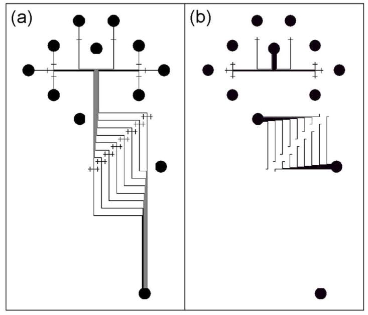
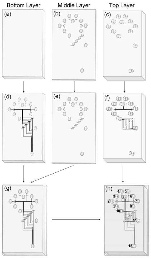
A schematic of the micropatterns formed in the different layers of the multilayer PMMA devices is shown in Figure 1. Solutions inside microchannels run independently in the top and bottom layers, and connect (for the same solution) or mix (for different solutions) at the interlayer through-holes in the middle layer in the devices. To make our multilayer microdevices, we used a combination of protocols reported previously,29–31 including laser machining, photolithography, hot embossing, and thermal bonding. The fabrication flow process is shown in Figure 2. Three PMMA layers with different thicknesses were used. Sample reservoirs and interlayer through-holes were machined in the middle sheet and sample reservoirs were made in the top layer using a laser cutter (Figure 2b-c)). Then, microchannels with the patterns in Figure 1 were imprinted onto the upper surface of the bottom layer and the lower surface of the top layer using hot embossing (Figure 2d, f). Subsequently, the middle layer with interlayer through-holes and reservoirs, and the bottom layer with imprinted microchannels were bonded together thermally (Figure 2g). The interlayer through-holes in the middle layer were lined up with crossing channel markers in the bottom layer. Alignment precision to within 200 μm was needed for successful device fabrication, so a 7X magnifier was used to guide positioning to the needed tolerances (Figure 3, upper inset). Finally, the top layer was thermally bonded to the assembled middle and bottom layers (Figure 2h), with the alignment guided under the magnifier. Reservoirs are numbered in Figure 2h, and descriptions are given in the legend.
Figure 1.
Schematic of the micropatterns formed in the (a) upper surface of the bottom layer and (b) lower surface of the top layer of the multilayer PMMA devices.
Figure 2.
Flow process for multilayer microfluidic device fabrication. (a-c) Step I, laser cutting of openings. (a) 1.5-mm-thick PMMA bottom layer. (b) 0.5-mm-thick PMMA middle layer with laser-cut reservoirs (larger) and interlayer through-holes (smaller). (c) 3-mm-thick PMMA top layer with laser-machined reservoir holes. (d-f) Step II, hot embossing. (d) Bottom layer (upper surface) after hot embossing microchannels. (e) Middle layer is not imprinted and is the same as in (b). (f) Top layer after hot embossing microchannels on the lower surface. (g-h) Step III, thermal bonding. (g) Assembly of the middle and bottom layers through thermal bonding. (h) A completed device with top layer thermally bonded to the assembly in (g). Reservoirs 1–8 are sample inlets for different analytes. Reservoir 9 is the fluorescent label inlet. Reservoirs 10–12 are buffer inlet, injection waste and waste, respectively. During gated injection, reservoirs 1–9 were grounded, reservoirs 10 and 11 were floated, and reservoir 12 was maintained at +1600 V. During separation, reservoirs 1–10 were grounded, reservoir 11 was at +1000 V, and reservoir 12 was at +1600 V.
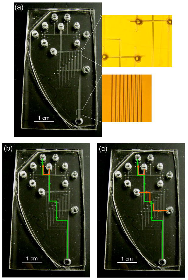
Figure 3.
Multilayer CAE microdevice photographs and operation. (a) Photograph of a complete device. (insets) Photomicrographs of interlayer through-holes (upper) and detection region (lower). The channels are ~40 μm wide and 13–15 μm deep. (b) The solution flow route during gated injection in one of the eight independent lanes is shown with arrows on green (bottom layer) and orange (top layer) solid lines. The interlayer through-holes are at the intersections of the green and orange lines. (c) The solution flow route during separation for the same lane is shown as in (b). See the text for additional details on device operation.
Batch processes (laser cutting and Si template microfabrication) that led to material for many finished devices required less than 5 min process time for each completed PMMA microchip. The combined steps of hot embossing and thermal bonding took ~70 min per PMMA device, which is still several times faster than the typical glass wafer bonding process time of ~4 hr per device. Figure 3 shows a photograph of a successfully constructed multilayer CAE microdevice with inset photomicrographs of alignment at interlayer through-holes and of the detection region.
Apparatus and Operation
An inverted optical microscope coupled with a laser induced fluorescence detection system was used, similar to what we reported previously.31 The multilayer microdevices were affixed above the objective in the microscope, as described in an earlier report.12 Two power supplies controlled sample loading and electrophoresis by providing voltages to a switching box controlled by LabView for gated injection.12,32 The switching box was connected to platinum wires inserted into the solution-filled reservoirs to provide electrical contact. The default configuration was separation mode, and injection times from 0.1 to 10.0 s could be programmed. In this paper, injection times of 1.0 s were used.
Solution flow during injection and separation in a non-multilayer design was described previously.12 In the present paper, our devices have a 3-layer design that provides on-chip fluorescent labeling and CAE separation of up to eight different samples simultaneously. The fluorescent label flowing in the top layer from reservoir 9 (see Figure 2h) and the protein analyte solutions traveling in the bottom layer from reservoirs 1–8 were mixed continuously from the junctions at the bases of the interlayer through-holes down to the injection intersections, during both injection and separation periods. During the 1.0 s gated injection, each labeled protein sample traveled a short distance down its respective separation column in the bottom layer while reservoirs 10 and 11 were floated. Once separation mode was resumed with the appropriate potentials applied to the reservoirs, each of the 8 mixed, uninjected samples once again flowed to injection waste (reservoir 11). The field in the separation channels then separated each of the loaded plugs of samples electrophoretically. The solution flow routes in one lane during separation mode are highlighted with green and orange lines having arrows in Figure 3. Voltages applied to the reservoirs during separation and injection are given in the Figure 2 legend. Photomicrographs of interlayer through-holes and the detection region (Figure 3) were captured using a Nikon D 90 (Tokyo, Japan) digital camera mounted on the microscope. We were initially concerned about the possibility of air bubble entrapment at interlayer through-holes during buffer filling, but this issue was not generally encountered in our experiments.
Parallel Analysis of BSA
The buffer in the microdevice was 10 mM sodium bicarbonate (pH unadjusted) containing 1 mM CTAB. For control experiments, 1.5 μL of dye stock solution was added to 20 μL of buffer; after 10 min, 10 μL of this diluted solution was delivered into reservoir 9 (Figure 2h), while buffer lacking protein was placed in the sample reservoirs. For parallel on-chip labeling and separation of BSA in eight lanes, 10 μL aliquots of a 20 μg/mL BSA solution in buffer were delivered into each of reservoirs 1–8. A diluted dye solution was made as in the control experiments and was immediately transferred into reservoir 9. The device was run in separation mode for 4–6 min to ensure that the dye and protein samples had mixed and migrated to the injection intersections. Then, microchip CAE was performed using a 1.0 s gated injection as described above.
HSP90 Detection Limit
We used 2.5 mM borate buffer (pH 8.0) containing 1 mM CTAB to fill devices and make protein solutions. Three HSP90 solutions of different concentrations (11.0, 5.50 and 2.75 μg/mL) were delivered into sample reservoirs 3–5 (Figure 2h). A diluted dye solution containing 4 μL of dye stock solution and 8 μL of buffer was transferred into reservoir 9. Electrophoresis was then carried out as above for the BSA samples.
On-chip Labeling and Separation of Protein Mixtures
The buffer used was the same as for the detection limit experiments. Reservoirs 1–2 had 25 μg/mL CytC, reservoirs 3–5 contained a mixture of 25 μg/mL CytC and 11 μg/mL HSP90, reservoirs 6–7 had 11 μg/mL HSP90, and reservoir 8 contained only running buffer. All other aspects of the experiment were the same as for HSP90 alone.
Fluorescence Detection
An air-cooled Ar ion laser (Laser Physics, West Jordan, UT) was used to generate the 488 nm excitation light; the power incident on the microchip was 3.5–4.7 mW for CAE experiments. For illuminating all eight separation lanes, the laser spot was increased to a ~1.5 mm diameter by passing a converging beam from a 10× beam expander through a 4×/0.13 NA objective. The laser beam was positioned 1–3 mm from reservoir 12 (see Figure 2h). Collected fluorescence went through a D600/60 band-pass filter (Chroma, Rockingham, VT) and was detected by a Photometrics CoolSNAP HQ cooled CCD camera (Photometrics, Tucson, AZ). 12-bit pictures were captured every 600 ms for 100 frames in each microchip CAE run and were processed by Image J software.
Data Analysis
After a CAE run, a time sequence image of the lanes was generated from the series of collected CCD images using a MatLab program written in house. First, a rectangular area of interest (AOI) was defined to be 1500-μm-tall and 750-μm-wide, covering all 8 lanes and located at the center of the laser illumination area. Next, mean intensity values of the pixel rows inside the AOI were calculated by first averaging the intensity values of each pixel row in the AOI, and then subtracting the average background values (obtained from the first 10 CCD images). Finally, all calculated mean intensity values of pixel rows from a 100 CCD image sequence became the signal columns in time-order to form the final image.
The electropherogram of each separation lane in a run was calculated from the collected CCD image sequence using Image J software. First, a rectangular AOI was defined to be 40 μm × 750 μm, which is the approximate width of a channel and one half the laser illumination diameter. This AOI was centered on the selected lane, and the mean value of pixel intensity inside the AOI for each frame was determined. Lastly, this mean intensity was plotted vs. frame number (running time) to produce an electropherogram for the lane.
Results and Discussion
Microdevice Design
In our previous report detailing on-chip labeling and separation of single samples,12 the fluorescent label reservoir and sample reservoir led to a 300-μm-wide, 4.7-mm-long reaction chamber. When protein sample and fluorescent label flowed electrophoretically through the reaction chamber, the wider channel slowed the solution velocity, increasing the reaction time. Although this approach worked well for one sample, it scales poorly for independent and simultaneous analysis of multiple samples on the same device. Indeed, placement of more than 2–3 such layouts becomes problematic for a compact planar device platform. Therefore, expansion to a third dimension is necessary.
In our layout, some microchannels are discontinuous, and features are distributed into two different layers, as shown in Figure 1. Solution streams flow independently in their respective layers, but join together at tiny (~100–200 μm diameter) interlayer through-holes in a middle layer, as shown in Figure 2b. The 0.5-mm-thickness middle layer was selected to decrease the interlayer through-hole volume to as small as 4 nL. Channel crossings in the bottom and top layers (Figure 1a-b) and channel turns in the top layer (Figure 1b) serve as alignment marks to indicate the locations of the interlayer through-holes. These extended connectors increase the likelihood of forming a fluidic connection between channels and through-holes during bonding.
Figure 2h and Figure 3a show a schematic and photograph of a completed device, respectively. The voltage configuration and solution flow routes (Figure 3b–c) are analogous to single-layer, single-lane microdevices reported previously for on-chip labeling and separation of proteins.12 In our parallel array design, a single inlet (reservoir 9) provides fluorescent label to all of the independent lanes. The sample inlets, reservoirs 1–8, allow up to eight different samples to be analyzed simultaneously. The interlayer through-holes serve not only as liquid connectors between the protein sample and dye inlets, but also to aid in the on-chip labeling reaction, as follows. First, the two solution streams meet where there is a larger interfacial area at the through-holes, which enhances their mixing through increased potential for convection. Second, since the streams combine vertically rather than horizontally, the short vertical distance (<15 μm channel depth compared to ~40 μm width) for diffusional mixing enables a faster reaction.
Parallel Analysis of BSA
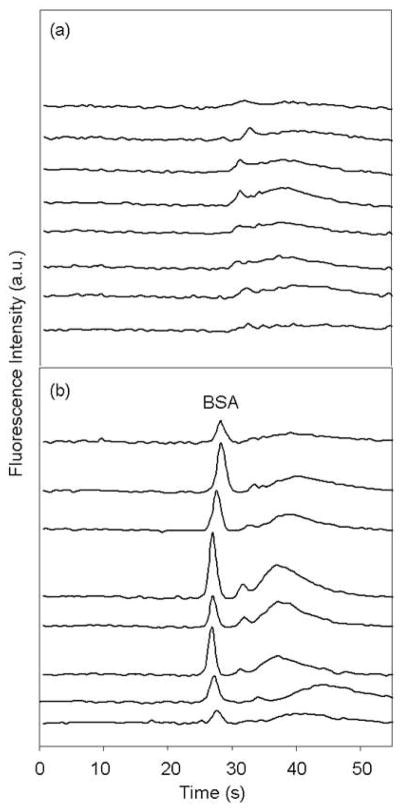
Figure 4 shows microchip electropherograms in all lanes after injection of CE dye 503 only and following injection of 20 μg/mL BSA that was labeled on-chip with CE dye 503. CTAB was present to prevent dye adsorption to device walls, as reported previously.12 Importantly, the system peaks and background resulting from CTAB are much less noticeable (Figure 4a) in our optimized approach described here than in previous work.12 When BSA was placed in the sample reservoirs, the on-chip labeled BSA peak appeared in all eight lanes well above the dye background (Figure 4b). Variations in protein peak signals between the middle and edge lanes are partially due to non-uniformity of the intensity of the expanded excitation laser beam. This issue could be addressed readily by optimizing the beam shape in the setup. Peak heights varied between lanes by a factor of up to 2.5 after adjusting for laser power. These differences are common in capillary array experiments19 and are most likely caused by minor variations in channel flow paths (and hence resistances) that affect injection efficiency. Slight misalignments between layers and small differences in through-hole dimensions are the most probable sources of channel resistance differences. We note that if needed, higher accuracy for quantitative work could be obtained through calibrating a device by running different standards in the individual lanes. Importantly, Figure 4 clearly demonstrates two key facts: first, simple and efficient on-chip labeling can be achieved through the interlayer through-hole design; and second, up to eight samples can be analyzed quickly and independently at the same time using our multilayer devices.
Figure 4.
Microchip electropherograms in 8 lanes after injection of (a) CE dye 503 only and (b) 20 μg/mL BSA labeled on-chip with CE dye 503. Electropherograms are offset vertically for clarity. The broad system peak (30–50 s) is from dye-CTAB complexes in the running buffer as reported previously.12
Detection Limit of HSP90
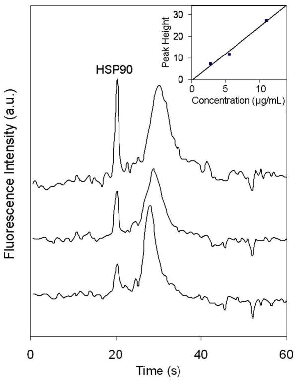
With our parallel approach, multiple analyses (e.g., limits of detection) can be done simultaneously, which could be a significant cost advantage. Figure 5 shows microchip electropherograms of different concentrations of HSP90 labeled on-chip with CE dye 503 in three adjacent lanes. Lanes 3–5 in the detection region (inset of Figure 3) were positioned at the center of the laser radiation, where the flat top region of intensity in the beam profile minimized differences in excitation applied to the three lanes. The baselines of the three electropherograms were also normalized to a common value to further account for any minor remaining influence of differences in excitation power on fluorescence signal. The background is slightly noisier in Figure 5 than Figure 4, most likely because a different buffer was used in these experiments. Based on the inset plot of HSP90 concentration versus peak height in Figure 5, the concentration detection limit was calculated to be 600 ng/mL, which is about a two-fold improvement over the 1 μg/mL detection limit reported in our previous work.12 The detection limit could be further improved at least ten fold to reach normal serum HSP90 levels (~20 ng/mL)33,34 by increasing signal-to-noise ratio through raising excitation power; improving beam shape (e.g., line focusing); using larger through-holes; spatial filtering of the detector signal; and optimizing buffer conditions, dye concentration and CCD frame capture rate.
Figure 5.
Microchip electropherograms of different concentrations of HSP90 labeled on-chip with CE dye 503 in three adjacent lanes. Offset traces from bottom to top are 2.75, 5.50, and 11.0 μg/mL HSP90. The gated injection time was 1.0 s. (inset) Plot of HSP90 concentration vs. peak height. The detection limit (3σ) was calculated to be 600 ng/mL. The slope is 2.48 with a standard deviation of 0.40, while the intercept is −0.6 with a standard deviation of 1.6. The broad system peak at ~30 s is explained in the Figure 4 legend.
On-chip Labeling and Separation of Different Protein Mixtures
To optimize conditions for resolution of HSP90 and CytC, we adjusted the buffer composition and pH, size of the interlayer through-holes, concentration of CTAB, and labeling time. Better separations were obtained from mildly basic (pH 8.0–8.5) than more strongly basic (pH 9.5–10.0) buffers. Borate buffer was preferred over sodium bicarbonate because it provided better separation efficiency, despite the slightly nosier background. Larger through-holes resulted in more complete labeling but reduced separation efficiency. Lower CTAB concentrations gave a cleaner background but resulted in a decrease in the reaction rate and separation efficiency.
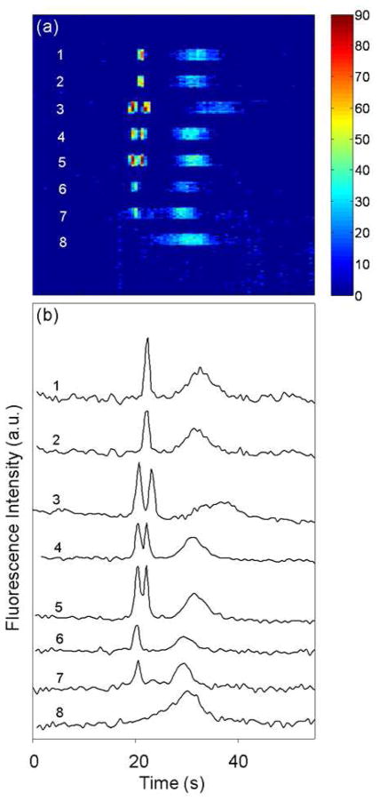
Figure 6 shows a time sequence of CCD data from the detection zone and the resulting electropherograms for different protein samples labeled on-chip and separated in an 8-lane microdevice. These results demonstrate successful parallel on-chip labeling and analysis of multiple, distinct protein samples in a microfabricated device. The protein peaks were well resolved in lanes 3–5 where mixtures were present, and all peaks were well above background signal levels (i.e., lane 8). Very small differences in migration times and signals between lanes can be attributed to the factors discussed above. Furthermore, no cross-talk between signals is observed in adjacent lanes. Importantly, our devices have the ability to analyze up to 8 different samples at the same time, with the labeling integrated on-chip and in parallel. These increased throughput and integrated microdevices show great promise for high-throughput biomolecule analysis in drug discovery and disease detection, for example.
Figure 6.
Separation of protein samples labeled on-chip in an 8-lane microdevice. (a) Time sequence image of CCD data from the detection zone. Protein peaks appear at ~20 s. Lanes 1–2 are 25 μg/mL CytC, lanes 3–5 are a mixture of 25 μg/mL CytC and 11 μg/mL HSP90, lanes 6–7 are 11 μg/mL HSP90, and lane 8 is a blank with only the fluorescent label. (b) Vertically offset electropherograms extracted from the CCD data in (a). The broad system peak at 30–40 s is explained in the Figure 4 legend.
Unlike some CAE designs,16,21 which use individual solution inlets for each lane, our layout contains only one fluorescent label reservoir and one set of electrophoresis reservoirs (buffer inlet, buffer waste and separation waste). All of the 8 independent on-chip labeling and separation units for different analytes share the same dye and electrophoresis reservoirs, thus requiring a total of only 12 reservoirs, or N + 4, where N is the number of different samples to be analyzed. In contrast, without a multilayer design an 8 sample device layout would require a total of 40 reservoirs, or 5N. We note the facile scalability of our design to larger sample numbers; for example, a 10 cm × 10 cm layout, readily achievable with standard cleanroom equipment, could easily accommodate 50 samples. Somewhat more advanced 15 cm diameter lithographic capabilities would allow for the analysis of 96 samples in parallel on a device with 100 reservoirs, a level of input complexity easily addressed in 96-well plates.
Conclusions
We developed multilayer PMMA devices that integrate on-chip fluorescent labeling with high-throughput protein analysis of up to eight different samples in parallel. There are a total of twelve reservoirs in each device: eight sample reservoirs, one fluorescence label reservoir and three electrophoresis reservoirs. Microchannels are imprinted into independent top and bottom PMMA layers through hot embossing, and connections are formed via interlayer through-holes machined with a laser cutter in a thin middle layer. Combining the three micromachined substrates together through thermal bonding forms the device. All sample reservoirs are fluidically connected via microchannels and interlayer through-holes to the dye reservoir for on-chip labeling. Using our fast and straightforward labeling protocol, individual proteins and protein mixtures have been successfully labeled on-chip and separated in parallel in multilayer devices, with a detection limit of 600 ng/mL for HSP90.
Besides the rapid analysis of multiple protein samples at the same time, several other potential applications for our devices are envisioned. For example, the same sample could be tagged with different labels or analyzed under different conditions simultaneously using our parallel (rather than serial) approach, which could save time and reagents. Peak sizes and positions may further illuminate the interaction mechanism between the sample and different labels. Alternatively, our devices would enable the analysis of the same sample using multiple separation techniques simultaneously, to find the optimal method or conditions rapidly, and with reduced analyte consumption. With N + 4 scaling for the total number of reservoirs needed, ~100 samples could be analyzed in parallel on a device of reasonable size. Our integrated on-chip labeling capillary array electrophoresis microdevices increase the separation speed and throughput in miniaturized systems, enabling automation of biomolecule analysis.
Acknowledgments
This work was supported by a Presidential Early Career Award for Scientists and Engineers (PECASE) through the National Institutes of Health (R01 EB006124). Microfabrication of the Si templates was performed in the Integrated Microelectronics Laboratory at Brigham Young University.
References
- 1.Arruda DL, Wilson WC, Nguyen C, Yao QW, Caiazzo RJJ, Talpasanu I, Dow DE, Liu BCS. Expert Rev Mol Diagn. 2009;9:749–755. doi: 10.1586/erm.09.47. [DOI] [PMC free article] [PubMed] [Google Scholar]
- 2.Giljohann DA, Mirkin CA. Nature. 2009;462:461–464. doi: 10.1038/nature08605. [DOI] [PMC free article] [PubMed] [Google Scholar]
- 3.Oita I, Halewyck H, Thys B, Rombaut B, Vander Heyden Y, Mangelings D. Anal Bioanal Chem. 2010;398:239–264. doi: 10.1007/s00216-010-3857-7. [DOI] [PMC free article] [PubMed] [Google Scholar]
- 4.Myers FB, Lee LP. Lab Chip. 2008;8:2015–2031. doi: 10.1039/b812343h. [DOI] [PubMed] [Google Scholar]
- 5.Yanik AA, Huang M, Kamohara O, Artar A, Geisbert TW, Connor JH, Altug H. Nano Lett. 2010;10:4962–4969. doi: 10.1021/nl103025u. [DOI] [PMC free article] [PubMed] [Google Scholar]
- 6.Wan D, Yuan SJ, Li GL, Neoh KG, Kang ET. ACS Appl Mater Interfaces. 2010;2:3083–3091. doi: 10.1021/am100591t. [DOI] [PubMed] [Google Scholar]
- 7.Thaxton CS, Elghanian R, Thomas AD, Stoeva SI, Lee JS, Smith ND, Schaeffer AJ, Klocker H, Horninger W, Bartsch G, Mirkin CA. Proc Natl Acad Sci U S A. 2009;106:18437–18442. doi: 10.1073/pnas.0904719106. [DOI] [PMC free article] [PubMed] [Google Scholar]
- 8.Arora A, Simone G, Salieb-Beugelaar GB, Kim JT, Manz A. Anal Chem. 2010;82:4830–4847. doi: 10.1021/ac100969k. [DOI] [PubMed] [Google Scholar]
- 9.Watson MWL, Jebrail MJ, Wheeler AR. Anal Chem. 2010;82:6680–6686. doi: 10.1021/ac101379g. [DOI] [PubMed] [Google Scholar]
- 10.Wheeler AR. Science. 2008;322:539–540. doi: 10.1126/science.1165719. [DOI] [PubMed] [Google Scholar]
- 11.Chatterjee D, Ytterberg AJ, Son SU, Loo JA, Garrell RL. Anal Chem. 2010;82:2095–2101. doi: 10.1021/ac9029373. [DOI] [PubMed] [Google Scholar]
- 12.Yu M, Wang HY, Woolley AT. Electrophoresis. 2009;30:4230–4236. doi: 10.1002/elps.200900349. [DOI] [PMC free article] [PubMed] [Google Scholar]
- 13.Wu JF, Ferrance JP, Landers JP, Weber SG. Anal Chem. 2010;82:7267–7273. doi: 10.1021/ac101182r. [DOI] [PMC free article] [PubMed] [Google Scholar]
- 14.Yang WC, Yu M, Sun XH, Woolley AT. Lab Chip. 2010;10:2527–2533. doi: 10.1039/c005288d. [DOI] [PMC free article] [PubMed] [Google Scholar]
- 15.Mathies RA, Huang XC. Nature. 1992;359:167–169. [Google Scholar]
- 16.Woolley AT, Sensabaugh GF, Mathies RA. Anal Chem. 1997;69:2181–2186. doi: 10.1021/ac961237+. [DOI] [PubMed] [Google Scholar]
- 17.Simpson PC, Roach D, Woolley AT, Thorsen T, Johnston R, Sensabaugh GF, Mathies RA. Proc Natl Acad Sci U S A. 1998;95:2256–2261. doi: 10.1073/pnas.95.5.2256. [DOI] [PMC free article] [PubMed] [Google Scholar]
- 18.Shi YN, Simpson PC, Scherer JR, Wexler D, Skibola C, Smith MT, Mathies RA. Anal Chem. 1999;71:5354–5361. doi: 10.1021/ac990518p. [DOI] [PubMed] [Google Scholar]
- 19.Emrich CA, Tian HJ, Medintz IL, Mathies RA. Anal Chem. 2002;74:5076–5083. doi: 10.1021/ac020236g. [DOI] [PubMed] [Google Scholar]
- 20.Pei J, Dishinger JF, Roman DL, Rungwanitcha C, Neubig RR, Kennedy RT. Anal Chem. 2008;80:5225–5231. doi: 10.1021/ac800553g. [DOI] [PMC free article] [PubMed] [Google Scholar]
- 21.Dishinger JF, Reid KR, Kennedy RT. Anal Chem. 2009;81:3119–3127. doi: 10.1021/ac900109t. [DOI] [PMC free article] [PubMed] [Google Scholar]
- 22.Pei J, Nie J, Kennedy RT. Anal Chem. 2010;82:9261–9267. doi: 10.1021/ac101755y. [DOI] [PubMed] [Google Scholar]
- 23.Ren KN, Liang QL, Mu X, Luo GA, Wang YM. Lab Chip. 2009;9:733–736. doi: 10.1039/b810705j. [DOI] [PubMed] [Google Scholar]
- 24.Becker H, Gartner C. Anal Bioanal Chem. 2008;390:89–111. doi: 10.1007/s00216-007-1692-2. [DOI] [PubMed] [Google Scholar]
- 25.Tsao CW, DeVoe DL. Microfluid Nanofluid. 2009;6:1–16. [Google Scholar]
- 26.Dang F, Shinohara S, Tabata O, Yamaoka Y, Kurokawa M, Shinohara Y, Ishikawa M, Baba Y. Lab Chip. 2005;5:472–478. doi: 10.1039/b417398h. [DOI] [PubMed] [Google Scholar]
- 27.Shadpour H, Hupert ML, Patterson D, Liu CG, Galloway M, Stryjewski W, Goettert J, Soper SA. Anal Chem. 2007;79:870–878. doi: 10.1021/ac0612168. [DOI] [PubMed] [Google Scholar]
- 28.Craig DB, Wetzl BK, Duerkop A, Wolfbeis OS. Electrophoresis. 2005;26:2208–2213. doi: 10.1002/elps.200410332. [DOI] [PubMed] [Google Scholar]
- 29.Fuentes HV, Woolley AT. Anal Chem. 2008;80:333–339. doi: 10.1021/ac7017475. [DOI] [PMC free article] [PubMed] [Google Scholar]
- 30.Kelly RT, Pan T, Woolley AT. Anal Chem. 2005;77:3536–3541. doi: 10.1021/ac0501083. [DOI] [PubMed] [Google Scholar]
- 31.Kelly RT, Woolley AT. Anal Chem. 2003;75:1941–1945. doi: 10.1021/ac0262964. [DOI] [PubMed] [Google Scholar]
- 32.Ermakov SV, Jacobson SC, Ramsey JM. Anal Chem. 2000;72:3512–3517. doi: 10.1021/ac991474n. [DOI] [PubMed] [Google Scholar]
- 33.Sun Y, Zang Z, Xu X, Zhang Z, Zhong L, Zan W, Zhao Y, Sun L. Int J Mol Sci. 2010;11:1423–1433. doi: 10.3390/ijms11041423. [DOI] [PMC free article] [PubMed] [Google Scholar]
- 34.Szerafin T, Hoetzenecker K, Hacker S, Horvath A, Pollreisz A, Arpad P, Mangold A, Wliszczak T, Dworschak M, Seitelberger R, Wolner E, Ankersmit HJ. Ann Thorac Surg. 2008;85:80–87. doi: 10.1016/j.athoracsur.2007.06.049. [DOI] [PubMed] [Google Scholar]


