Abstract
The property degradation observed in thin Pb(Mg1/3Nb2/3)O3-PbTiO3 (PMN-PT) crystals is believed to relate to large domains and subsequent clamping induced by surface-boundary. In this work, the properties were investigated as function of domain size, using controlled poling. The degraded piezoelectric and dielectric properties of thin PMN-PT were found to increase significantly, by decreasing domain size. Furthermore, the fine domain structure was found to be stable at 3kV/cm after 7.0×10⁵ negative-pulse cycles, hence, enabling PMN-PT crystals for high-frequency (>20 MHz) ultrasound-transducers.
Keywords: Crystalline oxides, electrical properties, dielectrics, piezoelectricity, ferroelectricity
I. Introduction
High frequency ultrasonic transducers (20–100MHz) are widely used in the area of medical diagnosis, such as dermatologic skin imaging, ophthalmic eye imaging, and catheter-based intravascular (IVUS) imaging owing to the higher imaging resolution1–3. One of the main limitations for high frequency imaging, however, is a shallow depth of field caused by increased attenuation with frequency. Improvements in signal-to-noise ratio (SNR) and transducer bandwidth help overcome limitations, which can be achieved with improvements in the piezoelectric transducer4–7.
Ferroelectric relaxor-PT single crystals, specifically Pb(Mg1/3Nb2/3)O3-PbTiO3 (PMN-PT), offer high dielectric (εr >6000) and electromechanical coupling (k33>0.9), which can be used to fabricate high-sensitivity, broad-bandwidth ultrasonic transducers. However, the dielectric and piezoelectric properties of PMN-PT single crystals have been reported to significant decrease with decreasing sample thickness (increasing operational frequency), limiting its performance in high frequency ultrasound10,11. It was speculated that the observed degradation was related to the relatively coarse domain size (> 20μm), which leads to polarization clamping as the sample thickness approaches its domain size. Therefore, it was hypothesized that finer domain PMN-PT crystals would result in improved piezoelectric and dielectric properties in the high frequency range. It has been reported that the evolution of the domain and growth of domain in ferroelectric materials can be controlled during poling with an appropriate electric field and temperature12,13; thus, it can be anticipated that relatively small domain size of PMN-PT crystals can be engineered with specific poling conditions.
In this work, fine domain PMN-PT single crystals were engineered with controlled poling, in order to minimize scaling effects observed in PMN-PT crystals. In addition, the stability of the fine domain structures and electrical properties of domain-size engineered crystals were investigated as a function of pulse-field and/or with increasing number of pulses (pulse cycle).
II. Experiment
The PMN-PT crystals used in this work were grown along the [100] direction using the modified Bridgman method14. Crystal samples with an area of 5×5 mm2 were polished to a thickness of ~100 microns. Semi-transparent gold electrodes were sputtered on the large surfaces to allow in-situ microscopic observation of the domain structures, and to allow electrical property measurements. Poling was done by applying an electric field along the [100] direction with different temperatures. The domain structure was subsequently investigated using a polarizing light microscope (Zeiss Axioskop) with a digital camera (Pixelink) connected to computer. The dielectric permittivity was calculated from the capacitance using an HP4284A multi-frequency LCR meter at 1kHz. Unipolar strain (S-E) was measured using a modified Sawyer-Tower circuit and linear variable differential transducer (LVDT), driven by a lock-in amplifier (Stanford Research Systems, Model SR830). The high field piezoelectric coefficient (d33) was determined from the slope of unipolar strain curve. An Olympus panametrics 200 MHz computer controlled pulser/receiver with a duration of 5 ns was employed to investigate domain stability.
III. Results and Discussion
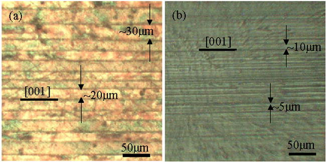
Fig. 1 shows the domain structure observed in [100] oriented PMN-PT crystals developed under different poling conditions. It can be seen from Fig. 1(a) that when the crystals were poled at room temperature, laminar domains with [001] boundaries were formed. The width of the domains varied from 20 micron to 30 microns. Utilizing a field-cooling method, in which the samples were heated to 260 C with an applied electric-field of 6kV/cm, followed by cooling to room temperature at 2 C/min, the domain structure in PMN-PT crystals was found to be significantly smaller, as shown in Fig. 2(b), with size varying from the maximum of 10 micron to less than 5 micron.
Fig. 1.

Domain structure in (a) room temperature poled and (b) field-cooled [100]-oriented PMN-PT crystals.
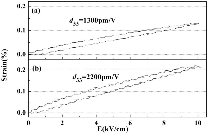
Fig. 2.
Unipolar strain as a function of electric field for (a) room temperature poled and (b) field cooling [100]-oriented PMN-PT crystals (sample thickness ~100μm).
The dielectric and piezoelectric properties of the sample with different domain size are reported in Table I. Also, reported are the values of thick samples with no degradation. It was found that the dielectric permittivity of fine domain PMN-PT crystals maintained a similar level (~6000) to the relatively thick (~1 mm) PMN-PT crystals. In contrast, the dielectric permittivity of the coarse domain (>20 micron) PMN-PT crystals showed significantly reduced properties, being on the order of 3000, when the thickness was reduced to 100 microns.
Table I.
The piezoelectric and dielectric properties in [100]-poled PMN-PT crystals as a function of domain size
| Poling condition | Domain size (μm) | Thickness (μm) | d33 (pC/N) | εr |
|---|---|---|---|---|
| Poled at 25°C/8kV/cm | >20 | 1000 | 1800 | 6000 |
| Poled at 25°C/8kV/cm | >20 | 100 | 1300 | 3000 |
| Field-cooling @ 6kV/cm | ~5 | 100 | 2200 | 5600 |
The unipolar strain behavior for fine and coarse domain PMN-PT crystals (~100μm) is presented in Fig. 2. It can be seen that the strain of the fine domain PMN-PT crystals was significantly higher than that of coarse domain crystals. The calculated high field d33s from the strain-field curves of the fine domain PMN-PT crystals were found to be about 2200 pm/V, with similar strain levels as observed in thick non-degraded PMN-PT crystals. In contrast, coarse domain PMN-PT crystals exhibited reduced strains, with piezoelectric coefficient being less than 1300 pm/V, as summarized in Table I.
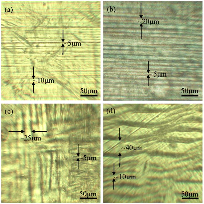
The stability of the engineered domain structure was further investigated by observing the domain structure as a function of pulse-field and number of cycles on the thin PMN-PT crystals. As shown in Fig. 3(a), the domain structure of PMN-PT crystals exhibited no noticeable change in the size and shape, after ~105 pulse cycles with amplitude on the order of 3kV/cm, higher than EC (~2kV/cm). The domain width was found to increase slightly, being on the order of 5–20μm, with further increasing pulse cycles (>107), as shown in Fig. 3(b). Fig. 3(c–d) shows the change in domain size and structure with increasing pulse cycles at 6 kV/cm (~3EC), from which, it can be observed that the domains broadened substantially with increasing pulse cycles, being on the order of 10–40 microns, similar to those observed in room temperature poled single crystals. It is believed that the enlarged domain structure may be due to the nucleation and growth of domains with increasing number of high-energy pulses.
Fig. 3.

Domain structure of PMN-PT crystals observed under various pulse conditions: (a) at 3kV/cm after 7.0×10⁵ pulses, (b) at 3kV/cm after 7.0×10⁷ pulses, (c) at 6kV/cm after 7.0×10⁵ pulses, (d) at 6kV/cm after 1.5×10⁶ pulses.
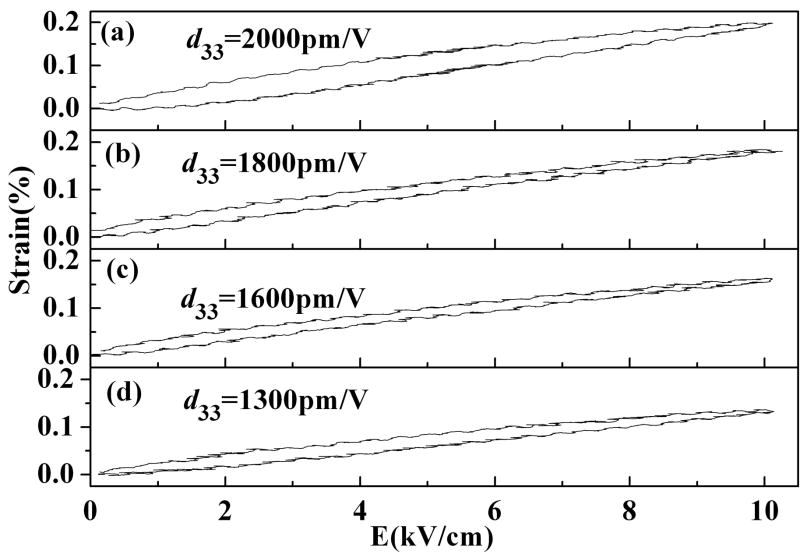
Fig. 4 shows unipolar strain behavior of PMN-PT crystals (thickness ~100μm) at a field of 10 kV/cm, after different pulse tests, where (a-d) correspond to average domain widths of 5, 10, 20 and 30 microns, respectively. The piezoelectric coefficient d33 calculated from the strain-field curves was found to be ~2000 pm/V (Fig. 4(a)) when relatively smaller domains were present, similar to non-degraded crystals. When the domains became broader after high-energy pulses, a decrease in the maximum strain level of PMN-PT crystal was observed as demonstrated in Figures 4(b–d). A similar trend was also observed for the dielectric properties: a decrease in dielectric permittivity with corresponding increased domain size, confirming that property degradation observed in thin plates are due to the domain size effects. The piezoelectric and dielectric properties of domain-size engineered PMN-PT crystals are summarized in Table II.
Fig. 4.
Unipolar strain of PMN-PT crystals as a function of electric field after pulse tests: (a) at 3kV/cm after 7.0×10⁵ pulses, (b) at 3kV/cm after 7.0×10⁷ pulses, (c) at 6kV/cm after 7.0×10⁵ pulses, (d) at 6kV/cm after 1.5×10⁶ pulses.
Table II.
Piezoelectric and dielectric properties in [100]-poled domain-size engineered PMN-PT crystals, as a function of pulse field and number of pulse cycles
| Pulse-field (kV/cm) | Pulse duration (ns) | Pulse cycle | Domain size (μm) | d33 (pm/V) | εr |
|---|---|---|---|---|---|
| Room Temperature Poling | 20~30 | 1300 | 3000 | ||
| 3 | 5 | 7.0×10⁷ | ~25 | 1300 | 3000 |
| 6 | 5 | 1.5×10⁶ | 20~32 | 1300 | 3000 |
| Field-cool Poling | 5~10 | 2200 | 5600 | ||
| 3 | 5 | 1.0×10⁵ | 5~10 | 2200 | 5600 |
| 3 | 5 | 3.5×10⁵ | 5~10 | 2200 | 5600 |
| 3 | 5 | 7.0×10⁵ | 5~10 | 2000 | 5500 |
| 3 | 5 | 7.0×10⁷ | 5~20 | 1800 | 5300 |
| 6 | 5 | 3.5×10⁵ | 5~10 | 2000 | 5500 |
| 6 | 5 | 7.0×10⁵ | 5~25 | 1600 | 4800 |
| 6 | 5 | 1.5×10⁶ | 10~40 | 1300 | 4100 |
IV. Summary
The dielectric and piezoelectric properties of PMN-PT crystals were found to degrade with decreasing sample thickness, owing to the large domain size (> 20μm) associated with the scaling effects from the sample surface boundary, greatly limited their applications in high frequency range (>20MHz). Field-cool poling approach was utilized to achieve significantly smaller domain size (~5μm), consequently leading to the improved dielectric and piezoelectric properties in thin crystal samples with thickness being on the order of <100 μm. The degraded piezoelectric d33 coefficients and dielectric properties in thin samples were found to increase from 1300 pm/V to 2200pm/V and 3000 to 5600, respectively, by drastically decreasing domain size. The engineered fine domain structure of PMN-PT crystals was found to be stable up to 3kV/cm (>EC) of a reverse pulse-field, after 7.0×10⁵ cycles, making PMN-PT crystals promising candidates for high frequency (>20 MHz) transducer applications.
Acknowledgments
The author (D. B. Lin) wants to thank the support from China Scholarship Council. Mr. E. W. Sun is acknowledged for helping the pulse tests. The authors from Xi’an Jiaotong University acknowledged the National Natural Science Foundation of China under Grant No.50872106 and National Basic Research Program of China (973 Program) under Grant No.2009CB623306 and International Science & Technology Cooperation Program of China under Grant No. 2010DFR 50480. The work supported by NIH under Grant No. P41-EB 21820 and ONR.
Footnotes
Publisher's Disclaimer: This is a PDF file of an unedited manuscript that has been accepted for publication. As a service to our customers we are providing this early version of the manuscript. The manuscript will undergo copyediting, typesetting, and review of the resulting proof before it is published in its final citable form. Please note that during the production process errors may be discovered which could affect the content, and all legal disclaimers that apply to the journal pertain.
References
- 1.Lockwood G, Turnball D, Christopher D, Foster F. IEEE Eng Med Biol Mag. 1996;15:60. [Google Scholar]
- 2.Turnbull D, Ramsay J, Shivji G, Bloomfield T, From L, Sauder D, Foster F. Ultrason Med Biol. 1996;22:845. doi: 10.1016/0301-5629(96)00107-x. [DOI] [PubMed] [Google Scholar]
- 3.Foster F, Pavlin C, Harasiewicz K, Christopher D, Turnbull D. Ultrason Med Biol. 2000;26:1. doi: 10.1016/s0301-5629(99)00096-4. [DOI] [PubMed] [Google Scholar]
- 4.Wang H, Jiang B, Shrout T, Cao W. IEEE Trans Ultrason Ferro Freq Control. 2004;51:908. doi: 10.1109/tuffc.2004.1320751. [DOI] [PubMed] [Google Scholar]
- 5.Jiang X, Snook K, Hackenberger WX. Geng, Proceeding SPIE. 2007;6531:65310F. [Google Scholar]
- 6.Jiang X, Snook K, Hackenberger W, Cheng A. J Xu IEEE Sensors. 2008:573. [Google Scholar]
- 7.Jiang X, Snook K, Walker T, Portune A, Haber R. Proceeding SPIE. 2008;6934:69340D. [Google Scholar]
- 8.Kuwata J, Uchino K, Nomura S. Jpn J Appl Phys. 1982;21:1298. [Google Scholar]
- 9.Park S, Shrout T. J Appl Phys. 1997;82:1804. [Google Scholar]
- 10.Lee H, Zhang S, Luo J, Li F, Shrout T. Adv Funct Mater. 2010;20:3154. doi: 10.1002/adfm.201000390. [DOI] [PMC free article] [PubMed] [Google Scholar]
- 11.Lee H, Zhang S, Shrout T. J Appl Phys. 2010;107:124107. doi: 10.1063/1.3437068. [DOI] [PMC free article] [PubMed] [Google Scholar]
- 12.Wada S, Yako K, Kakemoto H, Tsurumi T, Kiguchi T. J Appl Phys. 2005;98:014109. [Google Scholar]
- 13.Rao W, Xiao K, Cheng T, Zhou J, Wang Y. Appl Phys Lett. 2010;97:162901. [Google Scholar]
- 14.www.trstechnologies.com


