Abstract
We investigate the index sensing characteristics of plasmonic arrays based on square lattice slablike gold nanorings (NRs) with different ring widths. The gold NR arrays exhibit two extinction peaks in the visible and near-infrared corresponding to antibonding and bonding modes. Redshift and blueshift in antibonding and bonding modes when broadening the average ring width are observed. We experimentally demonstrate the sensitivity of bonding mode can be tuned by varying the average ring width. High sensitivity of 691 nm per refractive index unit is obtained for NRs with 199 nm average ring width.
During the last decade, the application of plasmonic technology based on periodic metallic nanostructures has attracted much attention since the advances in fabrication approaches for creating nanostructures. Localized surface plasmons (LSPs) are collective electron charge oscillations confined in metallic nanostructures. They exhibit enhanced near-field amplitude at the resonance frequency. These unique optical properties are being widely exploited in various applications, ranging from chemical, biological sensing1, 2 to subwavelength optical waveguides3, 4, 5 and surface-enhanced Raman scattering.6, 7 The resonance condition of LSPs sensitively depends on the sizes and geometries of the nanostructures.8 Up to date, optical properties of a train of nanostructure shapes have been explored, such as disks,9 spheres,10 prisms,11 cubes,12 rods,13 and crescents.14 In plasmonic sensing research, the increased sensitivity is achieved by using complex structures to obtain the plasmon hybridization15, 16 that results in the near-infrared (NIR) sensing, such as nanoshells,17 nanorice,18 and nanosandwiches.19 However, the sensing performance is limited because the enhanced fields concentrate inside the shell-like structures. The nanoring (NR) structure surmounts this limitation due to the extension of inside field to the environment. This leads to significant increase in the detection sensitivity.20 The NR plasmonic properties can be seen as the electromagnetic interaction between the nanodisc and the nanohole plasmons.21, 22, 23 This results in the splitting of the plasmon mode into two resonance modes, which are the low energy “bonding” mode and the high energy “antibonding” mode. The resonance frequencies of both resonance modes can be easily tuned in the visible (VIS) and NIR range by adjusting the geometry of NR, which is useful for various optical sensing applications.
In this letter, we report our experimental investigation of bonding and antibonding modes in plasmonic arrays based on square lattice slablike gold NRs with different ring widths. The refractive index sensing experiments of such structures are performed by immersing the samples in index matching liquids. We show that the sensitivities of NR arrays exhibit a linear relationship with ring widths for the bonding mode in the NIR regime. These results are crucial in designing LSP resonance (LSPR) sensors based on periodic metallic nanostructures.
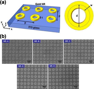
The scheme of square lattice gold NR array with ring thickness t, periodicity p, diameter d, and average width w is shown in Fig. 1a. The periodicity, diameter, and thickness are fixed at 1 μm, 500 nm, and 50 nm. In fabrication, the ITO glass is utilized as the substrate to avoid the charge accumulation effect during electron beam lithography (EBL). First, the ITO glass was spin-coated a 150 nm polymethylmethacrylate (PMMA) layer. The NR patterns with area of 300×300 μm2 and different ring widths were defined on the PMMA layer by EBL. After the development process, a gold thin film with thickness of 50 nm was deposited by thermal evaporation. Then the liftoff process is applied by rinsing the sample in acetone for a few hours. Figure 1b shows the scanning electron microscope (SEM) images of the fabricated square lattice gold NR arrays with different average ring widths. The average ring widths of NR-A to NR-E are 55, 81, 117, 149, and 199 nm.
Figure 1.
(a) Scheme of square lattice gold NR array design. The ring thickness, periodicity, diameter and width are t, p, d, and w, respectively. (b) Top-view SEM pictures of fabricated square lattice gold NR arrays (A–E) with average ring widths w of 55, 81, 117, 149, and 199 nm. The periodicity p of array is 1 μm, the ring diameter is 500 nm, and the ring thickness t is 50 nm.
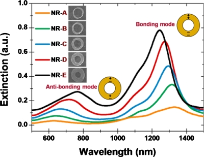
To obtain the transmission spectra of gold NR arrays, a halogen lamp was used. The light was focused on gold NR arrays through a 20× objective lens and the spot size is approximately 150 μm in diameter. The transmitted light was collected by another 20× objective lens and fed into a multimode optical fiber connected to an optical spectrum analyzer. The extinction spectrum was calculated using —log[Iout(λ)∕Iref(λ)], where Iout(λ) and Iref(λ) are the intensities of the transmitted light with and without the NR arrays. Figure 2 shows the measured extinction spectra of NR-A to NR-E. Gold NR arrays exhibit two strong optical resonances attributed to the hybridization of plasmons in the VIS-NIR region. The two resonance modes are identified as the antibonding and bonding modes. The observed shoulder in the spectral range between 1050 and 1150 nm can be ascribed to the high-order bonding mode. The charge distributions of the antibonding and bonding modes show the opposite and the same signs respectively at the inner and outer surfaces of the ring structure,23 shown as the insets of Fig. 2. The relatively lower peak intensity of the antibonding mode is due to the weakened localized field resulting from the opposite directions of attractive force in the NR structure. On the contrary, the same direction of attractive force in the bonding mode can enhance the localized field, leading to the higher peak intensity in extinction spectrum. The peak wavelengths of both resonance modes are strongly dependent on the NR width. For the bonding and antibonding modes, remarkable blueshift and redshift of 83 and 141 nm are observed by increasing the average ring width from 55 to 199 nm. This trend is in good agreement with the previously proposed model reported by Aizpurua et al.21 The observed ring width dependent behavior of the resonance peak can be interpreted by the plasmons coupling between the inner and outer surfaces of the NR structure.
Figure 2.
Measured extinction spectra of slablike gold NR arrays with different average ring widths. The insets show the charge distributions of the antibonding and bonding modes in the NR structure.
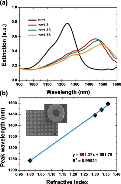
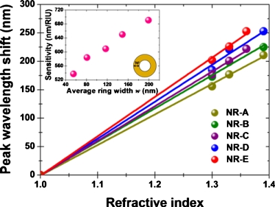
The index sensitivities of the gold NR arrays are measured by immersing the samples in index matching liquids (Cargille Laboratories) with different refractive indices from 1.30 to 1.39. For the NR-E array, the peak wavelength of the bonding mode shifts from 1244 nm to 1497 nm for refractive index varied from 1.00 to 1.36, as shown in Fig. 3a. The measured bonding mode wavelength of NR-E array as a function of the environmental index is shown in Fig. 3b. The sensitivity of gold NR array is estimated by finding the slope of the fitting curve using the least-square method. A very high sensitivity of 691 nm per refractive index unit (RIU) is obtained. In addition, the sensitivities of NR arrays with different average ring widths are also investigated, as shown in Fig. 4. The sensitivity of NR structure significantly increases from 537 to 691 nm per RIU when the average ring width was varied from 55 to 199 nm. The inset of Fig. 4 shows the sensitivity of NR array as a function of the average ring width. A linear relationship is obtained for the bonding mode in the NIR regime. The increased sensitivity with larger ring width can be explained by the resonance enhancement in the NR structure. From the pattern of charge distribution, the bonding mode can be regarded as a strong dipolar resonance. Increasing the ring width leads to the field enhancement because of the enlarged attractive force in the NR structure. This results in high index sensitivity to the change in surrounding dielectric environment. The sensitivities of other various LSPR index sensors ranging from 161 to 575 nm per RIU for nanosphere,24 nanoshell,25 nanowell,26 nanohole,27 and nanoslit28 structures are reported. For periodic metallic nanostructures with coherent interactions, the resonance line width can be reduced to achieve high sensing figure of merit. In addition, array types can offer extra spectral tunability and sensitivity enhancement. Therefore, the gold NR arrays with the obtained sensitivity up to 691 nm per RIU can be further improved by optimizing the NR array geometry29 and reducing the substrate effect.30
Figure 3.
(a) Measured extinction spectra of the NR-E array immersed in index matching liquids with different refractive indices. (b) Peak wavelength of the bonding mode of the NR-E array as a function of the environmental refractive index.
Figure 4.
Peak wavelength shift in the bonding mode of slablike gold NR arrays with different average ring widths immersed in index matching liquids with different refractive indices. The inset shows the sensitivity as a function of average ring width w for slablike gold NR arrays.
In summary, in this report, we demonstrate a plasmonic index sensor based on square lattice slablike gold NR array. The peak wavelengths of the antibonding and bonding modes are strongly dependent on the width of the NR. The redshift and blueshift in the antibonding and bonding modes when broadening the average ring width are experimentally observed. For the bonding mode, we show that the sensitivity can be improved by broadening the ring width because of the field enhancement. High sensitivity of 691 nm per RIU under the ring width of 199 nm is obtained. These observations strongly show that slablike gold NR array has great potential for the plasmonic sensing application. In addition, by adjusting the geometry of the gold NR array, we can easily obtain the bonding mode located around 1300 nm, which is a suitable wavelength for biomedical applications. Therefore, slablike gold NR array can serve as a highly sensitive, label-free, and chip-based optical sensor, which can be applied to fundamental studies of biological reaction processes, drug developments, diagnosis and treatment of human diseases.
Acknowledgments
This work is supported by Taiwan’s National Science Council (NSC) under Contract Nos. NSC-98-2221-E-009-015-MY2, NSC-99-2120-M-009-009, and NSC 98-3114-E-009-004-CC2. The authors would like to thank the help from Center for Nano Science and Technology (CNST) at National Chiao Tung University (NCTU), Taiwan. The author Chia-Yang Tsai would like to give his special thanks to Dr. Tsan-Wen Lu in Institute of Electro-Optical Engineering at NCTU, Taiwan, for his generous help and fruitful discussions.
References
- Stewart M. E., Anderton C. R., Thompson L. B., Maria J., Gray S. K., Rogers J. A., and Nuzzo R. G., Chem. Rev. (Washington, D.C.) 108, 494 (2008). 10.1021/cr068126n [DOI] [PubMed] [Google Scholar]
- Anker J. N., Hall W. P., Lyandres O., Shah N. C., Zhao J., and Van Duyne R. P., Nature Mater. 7, 442 (2008). 10.1038/nmat2162 [DOI] [PubMed] [Google Scholar]
- Wang B. and Wang G. P., Appl. Phys. Lett. 89, 133106 (2006). 10.1063/1.2357557 [DOI] [Google Scholar]
- Bozhevolnyi S. I., Volkov V. S., Devaux E., Laluet J. Y., and Ebbesen T. W., Nature (London) 440, 508 (2006). 10.1038/nature04594 [DOI] [PubMed] [Google Scholar]
- Jung K. Y., Teixeira F. L., and Reano R. M., J. Lightwave Technol. 25, 2757 (2007). 10.1109/JLT.2007.902100 [DOI] [Google Scholar]
- Haynes C. L. and Van Duyne R. P., J. Phys. Chem. B 107, 7426 (2003). 10.1021/jp027749b [DOI] [Google Scholar]
- Banaee M. G. and Crozier K. B., Opt. Lett. 35, 760 (2010). 10.1364/OL.35.000760 [DOI] [PubMed] [Google Scholar]
- Haynes C. L. and Van Duyne R. P., J. Phys. Chem. B 105, 5599 (2001). 10.1021/jp010657m [DOI] [Google Scholar]
- Hanarp P., Käll M., and Sutherland D. S., J. Phys. Chem. B 107, 5768 (2003). 10.1021/jp027562k [DOI] [Google Scholar]
- Okamoto T. and Yamaguchi I., Opt. Lett. 25, 372 (2000). 10.1364/OL.25.000372 [DOI] [PubMed] [Google Scholar]
- Millstone J. E., Park S., Shuford K. L., Qin L., Schatz G. C., and Mirkin C. A., J. Am. Chem. Soc. 127, 5312 (2005). 10.1021/ja043245a [DOI] [PubMed] [Google Scholar]
- Sherry L. J., Chang S. H., Schatz G. C., and Van Duyne R. P., Nano Lett. 5, 2034 (2005). 10.1021/nl0515753 [DOI] [PubMed] [Google Scholar]
- Brioude A., Jiang X. C., and Pileni M. P., J. Phys. Chem. B 109, 13138 (2005). 10.1021/jp0507288 [DOI] [PubMed] [Google Scholar]
- Unger A., Rietzler U., Berger R., and Kreiter M., Nano Lett. 9, 2311 (2009). 10.1021/nl900505a [DOI] [PubMed] [Google Scholar]
- Prodan E., Radloff C., Halas N. J., and Nordlander P., Science 302, 419 (2003). 10.1126/science.1089171 [DOI] [PubMed] [Google Scholar]
- Prodan E. and Nordlander P., J. Chem. Phys. 120, 5444 (2004). 10.1063/1.1647518 [DOI] [PubMed] [Google Scholar]
- Hao E., Li S., Bailey R. C., Zou S., Schatz G. C., and Hupp J. T., J. Phys. Chem. B 108, 1224 (2004). 10.1021/jp036301n [DOI] [Google Scholar]
- Wang H., Brandl D. W., Le F., Nordlander P., and Halas N. J., Nano Lett. 6, 827 (2006). 10.1021/nl060209w [DOI] [PubMed] [Google Scholar]
- Dmitriev A., Pakizeh T., Kall M., and Sutherland D. S., Small 3, 294 (2007). 10.1002/smll.200600409 [DOI] [PubMed] [Google Scholar]
- Larsson E. M., Alegret J., Käll M., and Sutherland D. S., Nano Lett. 7, 1256 (2007). 10.1021/nl0701612 [DOI] [PubMed] [Google Scholar]
- Aizpurua J., Hanarp P., Sutherland D. S., Käll M., Bryant G. W., and García de Abajo F. J., Phys. Rev. Lett. 90, 057401 (2003). 10.1103/PhysRevLett.90.057401 [DOI] [PubMed] [Google Scholar]
- Hao F., Larsson E. M., Ali T. A., Sutherland D. S., and Nordlander P., Chem. Phys. Lett. 458, 262 (2008). 10.1016/j.cplett.2008.04.126 [DOI] [Google Scholar]
- Ye J., Dorpe P. V., Lagae L., Maes G., and Borghs G., Nanotechnology 20, 465203 (2009). 10.1088/0957-4484/20/46/465203 [DOI] [PubMed] [Google Scholar]
- McFarland A. D. and Van Duyne R. P., Nano Lett. 3, 1057 (2003). 10.1021/nl034372s [DOI] [Google Scholar]
- Tam F., Moran C., and Halas N., J. Phys. Chem. B 108, 17290 (2004). 10.1021/jp048499x [DOI] [Google Scholar]
- Zhu S., Dua C., and Fu Y., Opt. Mater. (Amsterdam, Neth.) 31, 769 (2009). 10.1016/j.optmat.2008.07.014 [DOI] [Google Scholar]
- Brolo A. G., Gordon R., Leathem B., and Kavanagh K. L., Langmuir 20, 4813 (2004). 10.1021/la0493621 [DOI] [PubMed] [Google Scholar]
- Lee K. L., Wu S. H., and Wei P. K., Opt. Express 17, 23104 (2009). 10.1364/OE.17.023104 [DOI] [PubMed] [Google Scholar]
- Jiang H. and Sabarinathan J., J. Phys. Chem. C 114, 15243 (2010). 10.1021/jp1003598 [DOI] [Google Scholar]
- Dmitriev A., Hägglund C., Chen S., Fredriksson H., Pakizeh T., Käll M., and Sutherland D. S., Nano Lett. 8, 3893 (2008). 10.1021/nl8023142 [DOI] [PubMed] [Google Scholar]


