Abstract
The cross-strip imaging readout employs charge division, and centroiding, of microchannel plate charge signals detected on two orthogonal layers of sense strips to encode event X–Y positions and times. We have developed cross-strip detectors and fully parallel channel position encoding electronics. The front-end amplifiers utilize two 32-channel pre-amplifier ASICs that send signals to a full 64-channel 60 MHz ADC circuit followed by a FPGA event-processing board. Tests with a software Finite Impulse Response filter and centroiding algorithm demonstrate <10mm resolution with a 32mm cross-strip anode detector using low microchannel plate gain (∼106). The self-triggered event timing accuracy is 750 ps, and the system is capable of encoding photons at >1 MHz in combination with firmware-based FPGA centroiding algorithms.
Keywords: Photon counting, Microchannel plate, imaging
1. Introduction
In recent years we have implemented a variety of delay line image readout systems for high-resolution, large format, photon-counting microchannel plate (MCP) detectors in space instrumentation [1–3]. The cross-strip (XS) anode concept (Fig. 1) [4,5] employs many of the physical design techniques used for the delay line anodes. However, the XS anode works by charge division (rather than signal propagation time-delay) to achieve much higher spatial resolution and event-processing speed, while using MCP gain (5 × 10⁵) that is several orders of magnitude lower. The XS anode is a coarse (∼0.5mm) multi-layer metal and ceramic cross-strip pattern on an alumina substrate. On one surface of the substrate the conductors are fabricated as a set of fingers approximately 0.5mm wide. Then sets of insulating and conducting fingers are applied in the orthogonal direction such that 50% of the bottom layer is left exposed, while keeping the cross-talk between axes negligible. The top and bottom layers are used to collect the charge from the MCPs with equal charge sharing between the axes. The anodes made in this fashion are low outgassing and accommodate >800°C temperatures, and thus can be put into sealed tube UHV devices. The charge cloud size from the MCP is matched to the anode period so that it is collected on several neighboring fingers to ensure an accurately determined event centroid. Each finger of the anode is connected to a low-noise charge-sensitive amplifier and followed by subsequent analog-to-digital conversion of individual strip charge values. The center peak of the charge cloud determines the coarse position of the registered photon, and the charge cloud centroid may be calculated by a hardware or software sum and division. High accuracy event position centroids can be achieved at low MCP gain because the capacitance load is far lower on the individual strip amplifier ASIC channels compared with the noise on the high-speed amplifiers connected to high-capacitance load delay lines [7].
Fig. 1.
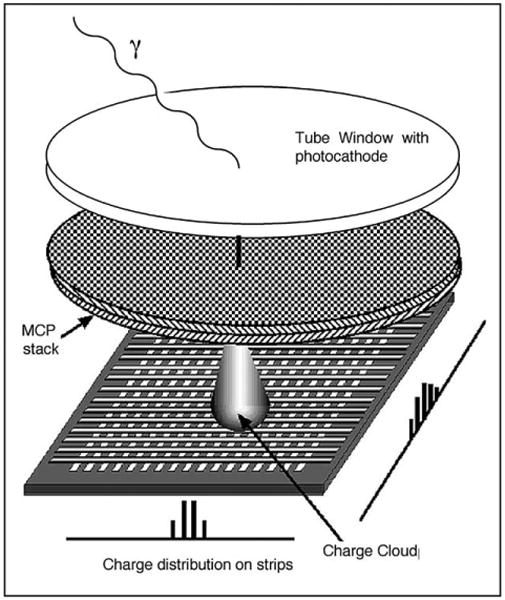
Schematic of a XS readout detector. Radiation interacts with a proximity-focused photocathode-producing photoelectrons, which are then multiplied by an MCP pair. The resulting electron cloud is divided between the strips on two orthogonal strip sets.
2. Cross-strip detectors
The basic scheme for XS anode detectors employs a photo-cathode, which converts incoming radiation to electrons, these are amplified by a stack of microchannel plates (MCP) and then detected on the readout anode (Fig. 1). Since the MCP gain required is far lower than for cross-delay line (XDL) anodes, only two MCPs are needed for XS anode detectors. XS anodes are typically mounted ∼2.5mm behind the MCP's. Each anode finger is connected through a hermetically sealed hole to the backside of the anode, allowing mounting of all the detector electronics outside the vacuum (Fig. 2). This allows the amplifier boards to be easily changed. The majority of our XS anode work [4,5] including a sounding rocket payload [6], has been done with a 32mm2 anode having 64 × 56 fingers for the top and bottom fingers, respectively. Anodes up to 50mm2 have also been made (Fig. 2), and smaller 22mm circular anodes have been constructed for use in sealed tube detectors [3]. The advantages of XS detectors include better spatial resolution at a substantially reduced MCP signal (gain) [7] that also results in proportionately longer detector lifetimes, and higher local event rate limits.
Fig. 2.
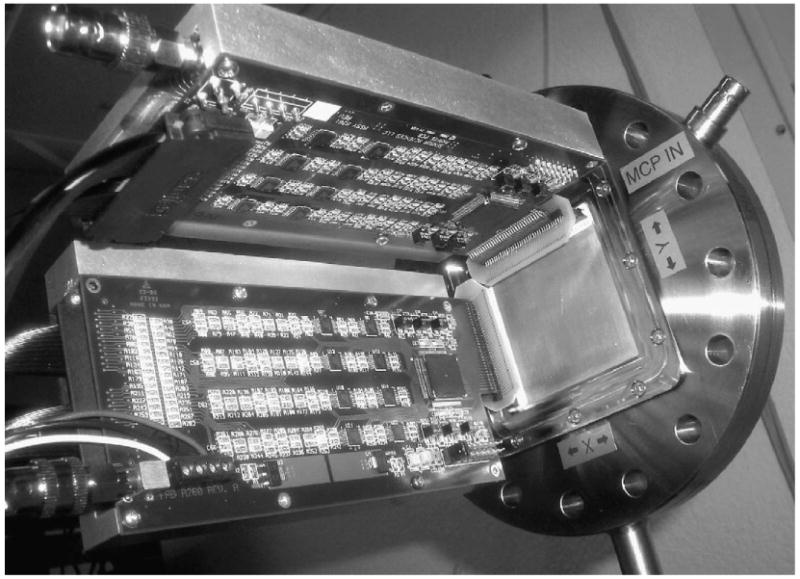
Photograph of a 40mm XS (50mm anode) detector showing the 64-channel amplifier boards (based on RD-20 ASIC) for X and Y connected to the back of the anode.
3. Image-encoding electronics
In our current approach, called the Parallel XS (PXS) electronics, each strip on the anode is connected directly to a preamplifier input of a 32-channel ASIC, the RD-20 amplifier [8], developed at the Rutherford-Appleton Laboratories. The output of these amplifiers are shaped unipolar pulses with ∼40 ns rise time, ∼200 ns fall time. The 64-parallel outputs (2 RD-20 ASICs on our front-end board, Fig. 2) are amplified again and transferred to a board (Fig. 3) where they are continuously digitized by 64 discrete 12-bit ADCs operating at 60 mega-samples per second (Msps). The digital samples are fed into an FPGA (Xilinx Virtex5) board where they are digitally Finite Impulse Response (FIR) filtered to extract pulse peak information. For each event the data for the set of affected neighboring strips is used to derive the event centroid(s) for both X and Y axes (one front-end amplifier board per axis). A time stamp is generated by the FIR filter allowing the correlation of X and Y positions for each event. This may be used to separate two or more events that are spatially separated, but nearly simultaneous events.
Fig. 3.
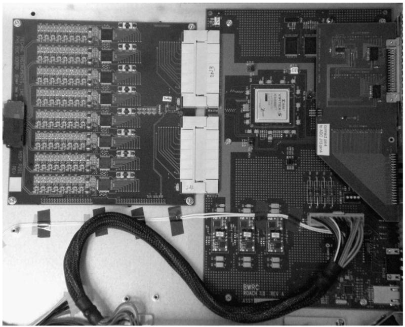
Photograph of the 64-channel, 60 MHz, ADC board (left) connected to the Xilinx Virtex-5 FPGA board (right) for digitization and processing of the amplifier signals.
The initial tests were performed with the 64-channel RD-20 boards, but using 8 ADC channels per axis with the 60 Msps (12 bits) ADCs interfaced to a PC where the algorithms were calculated in software. The flexibility of this system allows us to test and quickly optimize the digital processing algorithms to be subsequently implemented on the full 128 channel ADC-FPGA system. The electronics calibration [7] shows that the electronic noise in the RD-20 pre-amplifier ASIC is ∼900e− rms with the anode connected (∼10pF load) allowing spatial resolution of 5mm FWHM to be achieved at signals 3 × 10⁵ e−. Also the gain linearity of the amplifiers becomes non-linear for charges in excess of ∼1 × 10⁵e−. The electronics stimulation signal is not uniform across the 64 channels (Fig. 4) due to higher capacitive coupling at the channels at both ends when the chip is connected to the XS anode. The gain, gain linearity, and signal pedestal are all accommodated in lookup table corrections for each amplifier signal. Tests (Fig. 5) of the signal-processing algorithms show that timing of a detected event could be recovered from the digitized waveform on individual fingers with an accuracy of ∼750ps FWHM for signals above 105 e−. In single-event-driven mode the speed and data pipelined data processing in the FPGA can accommodate event rates of >1 MHz. We are also developing firmware to process multiple closely spaced (<200 ns) events that do not spatially overlap each other. This should allow event rates up to ∼5 MHz to be achieved, limited largely by the PC interface bandwidth. Multiple anodes can also be “mosaiced” into larger readout arrays while still accommodating the amplifier boards (5 cm × 15 cm) (Fig. 2). The ADC and FPGA circuits are currently mounted in 19″ standard racks, but this is only for our initial development phase, and can be conveniently repackaged into “NIM bin” style units in the future.
Fig. 4.
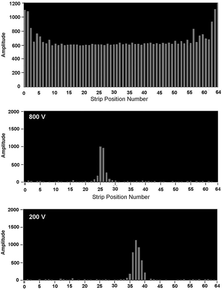
Top: measured signals for electronic stimulation of all 64 channels on one axis. Middle: single-event charge distribution for the 40mm detector using a 200V MCP-to-anode gap bias. Bottom: gap bias increased to 800V. 2.5mm gap, MCP gain 106.
Fig. 5.
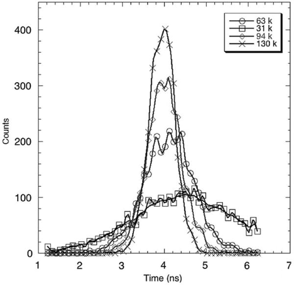
Timing jitter measurements for the electronics system as a function of input signal for generated stimulation pulses. At 1.3 × 10⁵ gain the jitter is 750 ps FWHM.
4. Cross-strip detector tests
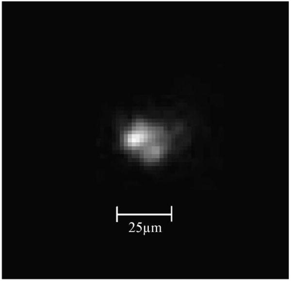
The RD-20 electronics system was evaluated using our 32mm XS detector [4] to image a test mask directly in contact with the top MCP having 10mm diameter pinholes illuminated with UV light. This detector uses a stack of two 10mm pore MCPs for amplification. Examples of single-event charge distributions are shown in Fig. 4, illustrating the narrowing of the electron cloud impinging on the XS anode as the MCP-to-anode gap bias is increased. Initial setup included incorporation of the gain, offset and linearity corrections for each amplifier channel, and optimization of the charge cloud size. Centroid calculations for each event then allowed the position data to be binned at small sampling scale (<2mm in this case) so that individual pinhole images can be seen as distinct point spread functions. The effective resolution (point spread function FWHM, Fig. 6) for two pinhole examples, improves with increasing signal as expected. However, because the MCP signal has a wide (60% FWHM) pulse amplitude distribution the detector resolution performance is worse than the electronic stimulation test data (Section 3). In addition the finite width of the MCP pores and their positions relative to the mask pinholes also contribute to the point spread function. For pinhole #1 the resolution limit is close to the 10mm pinhole and 10mm MCP pore size. For pinhole #2 the point spread function gets virtually no better above gains of 8 × 10⁵. The two-dimensional image (Fig. 7) of pinhole #2 shows that two MCP pores (12mm spacing) are illuminated through this 10mm pinhole, and are spatially resolved. This indicates that the intrinsic electronic resolution is <10mm and overall resolution is limited by the MCP pore size, as we have achieved in earlier tests [4,5,7] with previous electronics schemes.
Fig. 6.
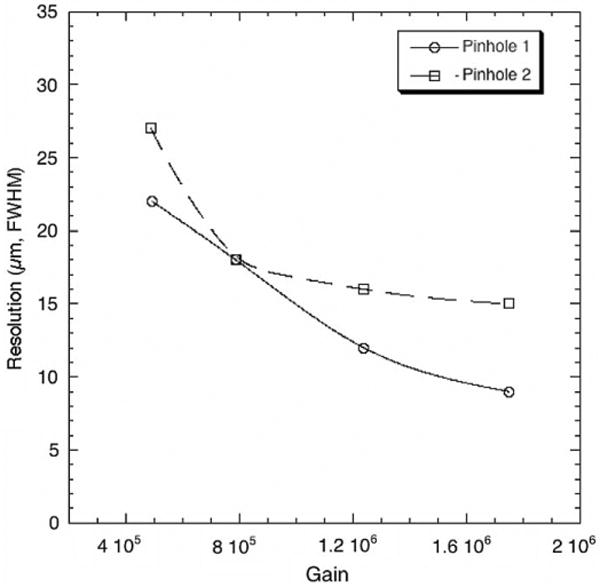
Image showing the resolved double image due to two MCP pores being illuminated by one 10 μm pinhole in the test mask.
Fig. 7.
Measurements of the image point spread function as a function of MCP gain for two 10μm pinholes in a test mask. MCP pores 10 μm diameter on 12.5 μm centers.
Acknowledgments
We wish to thank Mr. J. Hull, Mr. J. Malloy, Mr. C. Scholz and Mr. R. Raffanti for their contributions to this work. Portions of this work were supported by NASA under Grants NNG05GC79G and NNX08AE04G, NSF Grant DBI-0552-096 and NIH Grant NIBIB R01 EB006353.
References
- 1.Siegmund OHW, Jelinsky P, Jelinsky S, et al. Proc SPIE. 1999;3765:429. [Google Scholar]
- 2.Vallerga JV, Zaninovich J, Welsh B, Siegmund OHW, McPhate J, Hull J, Gaines G, Buzasi D. Nucl Instr and Meth A. 2002;477(1–3):551. [Google Scholar]
- 3.Siegmund OHW, McPhate J, Tremsin A, Vallerga JV, Welsh BY, Wheatley JM. AIP Conf Proc. 2008;984:103. [Google Scholar]
- 4.Tremsin AS, Siegmund OHW, Vallerga JV, Hull J. IEEE Trans Nucl Sci. 2004;NS-51(N4):1707. [Google Scholar]
- 5.Siegmund OHW, Welsh BY, Vallerga JV, Tremsin AS, McPhate JB. Proc SPIE. 2006;6220:53. [Google Scholar]
- 6.Berendse FB, Cruddace RG, Kowalski MP, Yentis DJ, Hunter WR, Fritz G, Siegmund O, Heidemann K, Lenke R, Seifert A, Barbee TW. Proc SPIE. 2006;6266:62660V. [Google Scholar]
- 7.Tremsin AS, Siegmund OHW, Vallerga JV, Hull JS. Proc SPIE. 2006;6276:627616. [Google Scholar]
- 8.Hall G. IEEE Trans Nucl Sci. 1994;NS-41(4 part 1–2):1086. [Google Scholar]


