Abstract
We report on a high resolution, monolithic crystal PET detector design concept that provides depth of interaction (DOI) positioning within the crystal. Our design utilizes a novel sensor on the entrance surface (SES) approach combined with a maximum likelihood positioning algorithm. We compare the intrinsic spatial resolution characteristics (i.e., X, Y and Z) using our SES design versus conventional placement of the photo-sensors on the rear surface of the crystal. The sensors can be any two-dimensional array of solid state readout devices (e.g., silicon photomultipliers (SiPM) or avalanche photodiodes (APD)). SiPMs are a new type of solid-state photodetector with Geiger mode operation that can provide signal gain similar to a photomltipiler tube (PMT). Utilizing a multi-step simulation process, we determined the intrinsic spatial resolution characteristics for a variety of detector configurations. The SES design was evaluated via simulation for three different two-dimensional array sizes: 8×8 with 5.8×5.8 mm2 pads; 12×12 with 3.8×3.8mm2 pads; and 16×16 with 2.8×2.8 mm2 pads. To reduce the number of signal channels row-column summing readout was used for the 12×12 and 16×16 channel array devices. The crystal was modeled as a 15 mm monolithic slab of a lutetium-based scintillator with the large area surface varying from 48.8×48.8 mm2 up to 49.6×49.6 mm2 depending upon the dimensions of the two-dimensional photo-sensor array. The intrinsic spatial resolution for the 8×8 array is 0.88 mm FWHM in X and Y, and 1.83 mm FWHM in Z (i.e., DOI). Comparing the results versus using a conventional design with the photo-sensors on the backside of the crystal, an average improvement of ~24% in X and Y and 20% in Z is achieved. The X, Y intrinsic spatial resolution improved to 0.67 mm and 0.64 mm FWHM for the 12×12 and 16×16 arrays using row-column readout. Using the 12×12 and 16×16 arrays also led to a slight improvement in the DOI positioning accuracy.
Index Terms: Continuous crystal, high spatial resolution, PET detector
I. Introduction
Tiscrete crystal detector modules have traditionally been used to achieve high spatial resolution for small animal positron emission tomography (PET) scanners [1–5]. However, cost goes up quickly as crystal cross-section gets smaller. We have previously investigated a continuous miniature crystal element (cMiCE) detector as a lower cost alternative to high-resolution discrete crystal designs. That detector consisted of a 50 mm by 50 mm by 8 mm slab of LYSO coupled to a 52 mm square, 64-channel flat panel photomultiplier tube [6]. A statistics based positioning (SBP) algorithm is used to improve the positioning characteristics of the detector compared to standard or modified Anger positioning schemes [7]. To improve the decoding performance a maximum-likelihood (ML) clustering method was implemented to extract depth of interaction (DOI) information from the detector [8]. The description of the positioning algorithm is further described in the Detector Design and Methods section.
For a traditional PET detector, the photo-sensors are positioned opposite the entrance surface of the crystal or distal to the object being imaged. Our hypothesis is that using that design, the best DOI estimation for a monolithic crystal detector will occur in the back section of the crystal, while most interactions occur in the front section of the crystal. We propose investigate whether placing the photo-sensors on the entrance surface of the crystal can improve DOI positioning accuracy. This brings up the SES design. While there have been others that have used sensors on both sides of a monolithic crystal [9,10], our goal is to achieve similar DOI positioning accuracy while only requiring sensors on one surface of the detector thereby significantly reducing cost of implementation.
Enabling technology of the SES design are solid state photo-sensors, such as, silicon photomultipliers (SiPM) and avalanche photodiodes (APD). Both of these photo-sensors have relatively low attenuation to 511 keV photons making them suitable for placement on the front surface of the detector. In addition, they can potentially be housed in very compact packaging to limit any packing fraction issues associated with a full detector system. An added benefit is that both of these types of sensors can be operated in high magnetic fields, which enables the possibility of PET/MR multimodality imaging using the proposed design.
While the design will work for both APDs and SiPMs, we are working on the development of a SES PET detector using 2D arrays of SiPMs. SiPMs are a new type of photodiode with Geiger mode operation [11–13]. We prefer the SiPM devices over APDs because they provide higher gain (~105) and better timing characteristics for coincidence imaging. On the other hand, SiPM performance characteristics are still changing as manufacturers are still optimizing their fabrication procedures. This includes the general operating characteristics and the production of 2D arrays of sensors. Thus the primary goal of this work is not to determine the absolute intrinsic spatial resolution performance offered by the design but to compare the three dimensional (3D) intrinsic spatial resolution performance of the SES design versus conventional placement of the photo-sensors on the exit surface of the crystal. A secondary goal is to investigate whether row-column summing approaches can be used and still provide excellent positioning resolution characteristics. We also note that the sensor on the entrance surface idea was also recently introduced by Schaart [14] and has also been investigated by Maas using APDs [15].
II. Detector design and methods
A. Sensor on entrance surface (SES) design
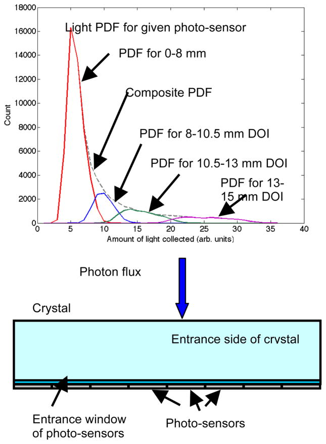
The following figures help to describe the SES concept. Fig. 1 shows a conventional design with the photo-sensors opposite the entrance surface of the crystal and what the light distribution probability density function (PDF) looks like for the photo-sensor directly under the photon flux (i.e., the thick vertical arrow). The composite PDF represents the amount of light collected by the selected photo-sensor for interactions occurring at different depths within the crystal. The linear attenuation coefficient of LYSO was used to determine the number of gamma interactions at each depth. For this proof of concept work, the results were not adjusted to account for the probability of Compton scatter within the crystal but just the depth of the first interaction point within the crystal. Along with the cumulative PDF, the plot is further separated into four depth regions using the known DOI information. As can be seen, for the traditional configuration, the peak of the PDF varies more significantly for events interacting at depths between 8–15 mm than for events interacting within 0–8 mm. Since our DOI estimation is based upon separation between the peaks of the PDFs for the different depth regions, we hypothesize that our DOI estimation is more accurate for regions where the amount of light collected is varying rapidly with depth. Therefore, we would ideally like most of the interactions to take place within depths 8–15 mm. However, because of the exponential interaction probability, a significant majority of the interactions occur within the first 8 mm of the crystal (68% of the first interactions occur in the 0–8 mm region and only 32% of interactions occur at depths between 8 and 15 mm) where visually we would expect the DOI discrimination to be the poorest.
Fig. 1.
Conventional design with the photo-sensors opposite the entrance surface of the crystal. The light PDF is a histogram, which shows the distribution of amount of light collected by a certain photo-sensor channel. The PDF for the photo-sensor directly under the photon flux (i.e., blue arrow) is shown.
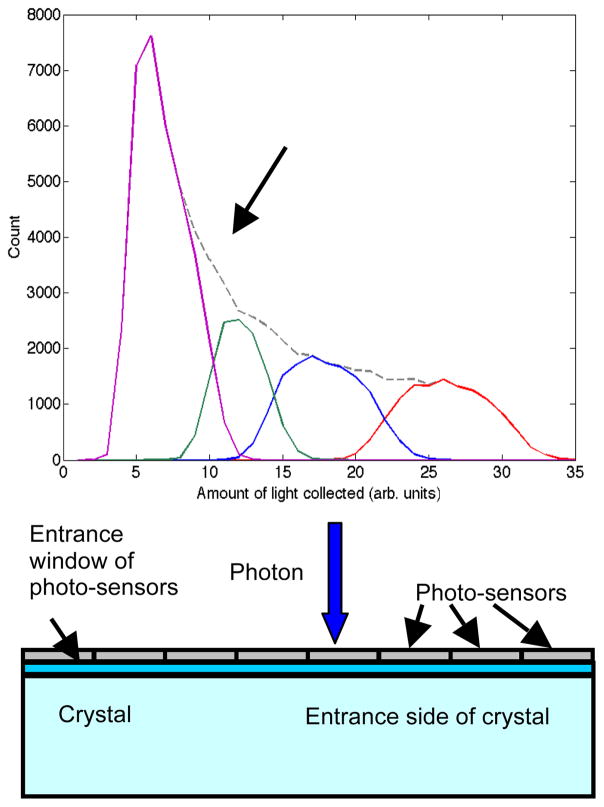
The fact that the majority of events were occurring within the opposite end of the crystal led to the SES design, as shown in Fig. 2. For the SES design the amount of the light collected varies more rapidly within the 0–5.5 mm region, where ~52% of the first interactions occur (16.5% occur in 0–1.5 mm region; 19.1% in the 1.5–3.5 mm region; and 16.1% occur in the 3.5–5.5 mm region). Therefore, the novel SES design has the potential to provide better DOI positioning performance.
Fig. 2.
SES design with photo-sensors on the entrance surface of the crystal. The PDF for the photo-sensor directly under the photon flux (i.e., blue arrow) is shown.
B. Statistics-based positioning (SBP) algorithm with DOI information [7]
If the distributions of observing signal outputs M = M1, M2… Mn for scintillation position x, are independent normal distributions with mean, μ(x), and standard deviation σ(x), the likelihood function for making any single observation mi from distribution Mi given x is:
| (1) |
The maximum likelihood estimator of the event position x is given by:
| (2) |
The SBP method requires that the light response function versus interaction location be characterized for the detector, where the light response function can be described by the mean number of light photons detected by a photo-sensor as a function of interaction position and the variance of the mean. SBP look-up tables (LUTs) corresponding to the mean and variance of the light probability density function (PDF) versus X,Y position are created during a characterization process.
To extend our SBP method for 3D positioning (i.e., DOI), we developed a maximum likelihood (ML) clustering method for extracting DOI information from a monolithic crystal [8]. The DOI separation technique divides the calibration data into different DOI regions. LUTs are then created for each DOI region. The full set of DOI LUTs allows the use of 3D ML positioning within our detector module. Our ML clustering technique has been used to extract up to 7 DOI regions from our 15 mm thick cMiCE detector. Based on the 7-depth DOI LUT, a third-order polynomial fit is applied to the mean and variance respectively for each (X,Y) position [16]. Then, a 15-depth DOI LUT is generated from the fit result.
The algorithm utilizes the fact that the light distribution pattern varies continuously and smoothly with DOI so scintillation events happening in similar DOI regions of the crystal will produce similar light distribution patterns. The 7-depth DOI LUT generation can be separated into five basic steps. For more details about the methodology see [8].
Step 1. For the training data at each position, the photo-sensor channel N receiving the maximum amount of light is located. The light histogram data for that channel is separated into seven initial groups according to their pulse height in photo-sensor channel N. Group 1 consists of events within the highest one-seventh of the PDF histogram, which correspond to interactions occurring closest to the photo-sensors in the crystal. Group 7 consists of events comprising the lowest one-seventh of the PDF histogram, which correspond to interactions occurring in the crystal region furthest from the photo-sensors.
Step 2. For each set of data (i.e., groups 1 through 7), the mean μ(j)i and standard deviation σ(j)i of the light response function are generated, where i is the number of the photo-sensor channel and j is the group number.
Step 3. For each event, the likelihood ratios between different groups are calculated and the event is placed in the most likely depth region. After all the data has been sorted, iterate by going back to Step 2.
Step 4. After a stable separation is reached, the final mean and standard deviation are generated where they represent the light response LUTs for DOI regions 1 through 7, respectively.
Step 5. For each (X,Y) position, a third-order polynomial fit is applied to the seven DOI means and standard deviations, respectively. A 15-depth DOI LUT is generated from the fitting results.
The idea behind the initial grouping in Step 1 is that the signal from channel N correlates with DOI. Based upon solid angle considerations, interactions near the photo-sensor window will have a larger amount of light collected by the photo-sensor channel directly under the interaction location than interactions further from the photo-sensor.
C. Simulation program for look up table (LUT) generation and testing
We utilize simulation tools that we have previously integrated to investigate different detector design alternatives. To summarize, DETECT2000 [17, 18] is used to determine the probability that a light photon generated at a specific (X, Y, Z) position in the crystal is detected by a specific photo-sensor. GEANT [19] is used to track the gamma interactions (both Compton and photoelectric) within the crystal. For each interaction, the number of light photons produced by the scintillator crystal is determined. That number is adjusted for the non-proportionality of LSO according to the tables reported by Rooney [20]. Poisson noise is then added to the number of light photons produced. Using the detection probabilities determined from the DETECT2000 simulations, the number of light photons striking each photo-sensor is determined. The number of light photons is then adjusted by the photon detection efficiency of the photo-sensor. Poisson noise is then added to the number of detected light photons. The number of light photons detected by each sensor for each interaction is summed for the final light distribution for a given event. Our current simulation does not include a model of the noise contribution from the photosensor. While noise from the photosensor will definitely effect performance for this work we are primarily interested in the DOI decoding benefits of the SES design and less focused on the exact characteristics of the photosensor that will be used with the design (e.g., SiPM or APD).
For the DETECT2000 simulations, the large area surface opposite the photo-sensors was modeled as being painted with white reflective paint (reflectivity coefficient of 0.98); the sides were modeled as being painted with black paint (reflectivity coefficient of 0.10). The scintillator material was modeled as producing 22,000 light photons per MeV. It was also modeled as having an index of refraction of 1.82. The index of refraction for the optical glue and the entrance window of the photo-sensor were 1.44 and 1.47, respectively. The photon detection efficiency (PDE) was set to 22.5%. This is similar to a PMT and within the range of PDE reported by different manufacturers of solid state photo-sensors. In general, APDs have much better quantum efficiencies, while the range of PDEs reported for SiPM devices varies between 4% up to ~50% at a wavelength of 420 nm [14,21]. It is worthwhile to note that the ~50% PDE reported by one manufacturer is not compensated for the effects of cross-talk and after pulsing. Using the simulation implementation and parameter values as listed for the 8 by 8 array, we measure an average energy resolution of 14% for the conventional design and 15.4% for the SES design.
D. Intrinsic spatial resolution testing
Three different photo-sensor array geometries were evaluated: 8 by 8 with 5.8 mm by 5.8 mm array elements with 6.08 mm center-to-center spacing; 12 by 12 with 3.8 mm by 3.8 mm pixels and 4.08 mm center-to-center spacing; and 16 by 16 with 2.8 mm by 2.8 mm pixels with 3.08 mm center-to-center spacing. Because the dead area between sensors was the same for each of the arrays, the 8 by 8 array has the best effective photosensor packing fraction. The crystal was modeled as a 48.8 mm by 48.8 mm by 15 mm slab of LYSO for the 8 by 8 sensor array and 49.2 mm by 49.2 mm by 15 mm for the 12 by 12 array; and 49.6 mm by 49.6 mm by 15 mm for the 16 by 16 array.
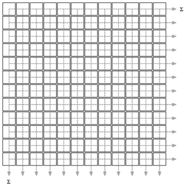
For the 8 by 8 array configuration the intrinsic spatial resolution characteristics were determined using the SES design and also for the conventional placement of the photo-sensors on the exit surface of the crystal. For the 12 by 12 and 16 by 16 pixel arrays, the intrinsic spatial resolution was determined using row-column summing (i.e., 24 and 32 channels). The 12 by 12 array configuration with row-column summing is illustrated in Fig. 3. The 15-depth DOI LUTs were built from photon fluxes with a diameter of 0.6 mm FWHM perpendicular to the face of the detector. A complete description on how the LUTs are generated is provided in [8]. The spacing between photon fluxes was 1.52 mm, 1.025 mm, and 1.55 mm in X and Y for the 8 by 8, 12 by 12 and 16 by 16 arrays, respectively. The LUT binning was 0.256 mm for the 12 by 12 photo-sensor array and 0.38 mm for the 8 by 8 and 16 by 16 arrays. Photon fluxes of normal incidence were used to train and test the X, Y and DOI positioning of the detector. The events were simulated as being a point flux for testing. Twenty thousand events were used for training. Ten thousand events were used for testing. A lower energy threshold of 400 keV was applied to the simulated data. Single (i.e., photoelectric only) and multiple (e.g., Compton plus photoelectric) interaction events were included for both the training and test data. The DOI resolution represents the error in the calculated DOI estimate versus the known first interaction point. The X and Y resolution was based upon the measured FWHM of the cumulative point spread function of all DOI layers summed together.
Fig. 3.
Sample 12 by 12 photo-sensor array readout using row and column summing.
III. Results
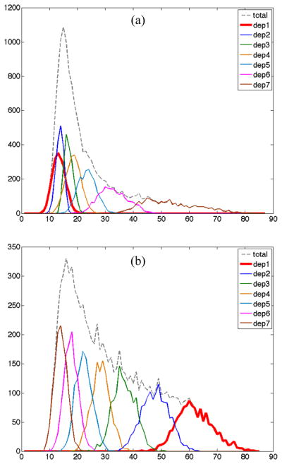
Sample depth separation results from our simulated data for both conventional placement of the sensor array on the backside of the crystal and for our SES design is illustrated in Fig. 4. For the conventional design, there is significant overlap of the light PDFs for depth regions 1–4, where a majority of events occur. Only regions 6 and 7 show good separation between the light PDFs. On the other hand, using the SES design, very good separation of the PDFs is observed for depth regions 1–4, where most of the interactions are occurring.
Fig. 4.
Depth separation results using a maximum likelihood clustering method [8] for: (a) conventional design and (b) SES design. Note that the thick line corresponds to the first depth region (i.e., the entrance region of the crystal).
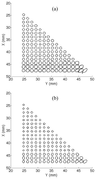
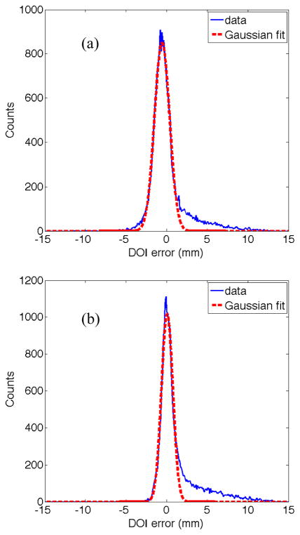
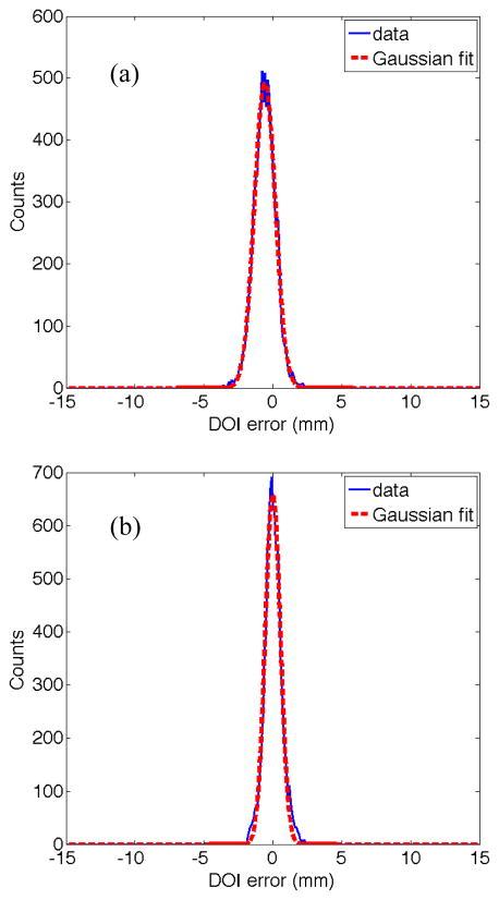
The two-dimensional contour plots illustrating the FWHM for normally incident photons for the 8 by 8 photo-sensor array geometries (i.e., SES and conventional) are illustrated in Fig. 5. The FWHM is directly measured from the positioned data results. Because of the symmetry of the detector, the results for one eighth of the detector are representative of the whole detector. The spacing between photon fluxes is 1.52 mm. A 15-depth DOI LUT was used for positioning. The SES design (Fig. 5b) shows about 24% better spatial resolution performance when compared to the conventional design (Fig. 5a). Excluding the last row and column at the edge of crystal the average intrinsic spatial resolution was 0.88 mm FWHM and 1.16 mm FWHM for the SES design and conventional design, respectively. Fig. 6 shows representative distributions of DOI positioning error. Doing a Gaussian fit, the average FWHM is 2.28 mm for the conventional design (Fig. 6a) and 1.83 mm for the SES design (Fig. 6b). The DOI positioning is slightly biased and has a tail. We believe the tails are a result of Compton scatter within the crystal and how it effects positioning. To test this hypothesis, we also determined DOI positioning without including the deleterious effects of Compton scattering in the detector. Those results are illustrated in Fig. 7. Without Compton scatter in the crystal, the tails of the DOI positioning error plot are gone and the DOI positioning resolution improved. For the results shown in the plots, the DOI resolution improved from 2.16 mm FWHM for the conventional design to 1.76 mm. For the SES design the FWHM improved from 1.62 mm to 1.27 mm. Therefore Compton scatter in the detector effects both X, Y and DOI positioning performance.
Fig. 5.
Contour plots of SBP positioning using 8 by 8 photo-sensor arrays with 15 depth DOI LUTs for: (a) conventional design; (b) SES design.
Fig. 6.
DOI resolution of SBP positioning using 8 by 8 photo-sensor arrays with 15 depth DOI LUTs for: (a) conventional design; (b) SES design.
Fig. 7.
DOI resolution of SBP positioning using 8 by 8 photo-sensor arrays with 15 depth DOI LUTs for: (a) conventional design; (b) SES design. Effects of Compton scatter in the detector were not included in the simulation. This confirms our hypothesis that the tails in the DOI positioning results are due to Compton scatter in the crystal.
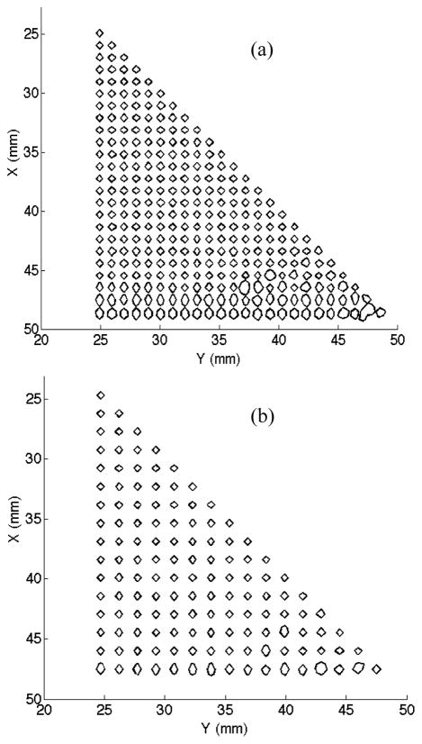
The two-dimensional contour plots illustrating the FWHM for normally incident photons for the 12 by 12 and 16 by 16 sensor array geometries are illustrated in Fig. 8. The results are for using row-column summing of the pixels. The spacing between photon fluxes is 1.025 mm for the 12 by 12 array detector and 1.55 mm for the 16 by 16 array detector. The X,Y intrinsic spatial resolution performance is similar for both array geometries, 0.67 mm FWHM for the 12 by 12 array and 0.64 mm FWHM for the 16 by 16 array. We believe that the reason the contour plots do not look circular is because the FWHM is on the order of the binning of our look up tables. The DOI positioning accuracy was also similar, 1.52 mm FWHM and 1.45 mm FWHM for the 12 by 12 and 16 by 16 photo-sensor arrays, respectively.
Fig. 8.
Contour plots of SBP positioning using 15 depth DOI LUTs for: (a) 12 by 12 photo-sensor array with 1.025 mm spacing between point fluxes; (b) 16 by 16 array with 1.55 mm spacing between point fluxes.
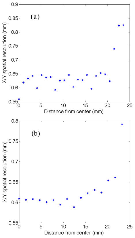
To get a better appreciation for how X, Y spatial resolution varies with position on the detector face, we also plot spatial resolution versus row-column distance from the center of the detector for the 12 by 12 and 16 by 16 array sensors in Fig. 9. For both arrays the spatial resolution stays quite constant until very near the edge of the detector. We believe the pattern for the 12 by 12 array detector is from points being located between rows or columns of sensors. Table I summarizes the intrinsic spatial resolution positioning results for the various detector configurations. The results are the average intrinsic spatial resolutions for the detector excluding the edge of the crystal. The first points were 1.52 mm, 1.025 mm and 1.55 mm from the edge of the crystal for the 8 by 8, 12 by 12 and 16 by 16 array configurations, respectively. The bias value represents the spatial difference between the location of the peak of the positioning results and the known test location. The fact that the bias is very small demonstrates that our positioning method is effectively not biased in X and Y.
Fig. 9.
X/Y spatial resolution as a function of distance from the center of crystal: (a) 12×12 array detector; (b) 16×16 array detector. Pattern for 12×12 array results probably a result of test points being between two rows or columns of sensors.
TABLE I.
Spatial resolution and positioning bias for different designs
| Design | Dimension | Bias (mm) | FWHM (mm) |
|---|---|---|---|
| 8×8 array (conventional) | X | 0.00 +/− 0.05 | 1.11 +/− 0.15 |
| Y | 0.01 +/− 0.04 | 1.21 +/− 0.17 | |
| DOI | −0.67 +/− 0.10 | 2.28 +/− 0.15 | |
| 8×8 array (SES) | X | 0.00 +/− 0.02 | 0.83 +/− 0.10 |
| Y | 0.00 +/− 0.04 | 0.92 +/− 0.14 | |
| DOI | 0.16 +/− 0.16 | 1.83 +/− 0.24 | |
| 12×12 array (SES, row-column) | X | 0.00 +/− 0.03 | 0.63 +/− 0.12 |
| Y | 0.01 +/− 0.05 | 0.70 +/− 0.13 | |
| DOI | −0.05 +/− 0.16 | 1.52 +/− 0.24 | |
| 16×16 array (SES, row-column) | X | 0.00 +/− 0.01 | 0.61 +/− 0.07 |
| Y | 0.00 +/− 0.02 | 0.67 +/− 0.08 | |
| DOI | −0.03 +/− 0.11 | 1.45 +/− 0.10 |
IV. Discussion and Conclusion
For the 8 by 8 photo-sensor array studies, the SES design provided an improvement of ~24% in the X,Y intrinsic spatial resolution and ~20% in DOI positioning performance. Further, for DOI positioning the SES design was significantly less biased, where the bias is defined as the offset of the peak of the DOI error distribution from zero. Using the conventional design there is an average DOI bias error of 0.67 mm compared to only 0.16 mm using the SES design approach. This will lead to less DOI positioning error in the detector. The key factor is having a majority of the photon interactions occur in a region of the crystal where the light distribution PDF is varying most rapidly (i.e., where the DOI positioning resolution is the most accurate). The dimensions of the individual sensor elements for the 8×8 array correspond to the size of the PMT channels for the Hamamatsu H8500 multi-anode PMT (Hamamatsu, Japan). While the simulation results using the 8 by 8 photo-sensor array dimensions were very good, we are unaware of any 5.8 mm by 5.8 mm SiPM devices currently being made.
Further improvements in both X,Y and DOI positioning performance were obtained by using smaller pixel elements. These pixel sizes are more reflective of the largest SiPM devices currently being offered by manufacturers and are also becoming available in 2D array packages. For our simulation results, even when using row-column summing (which significantly reduces the number of signals channels that need to be collected) the positioning performance was better for the 12 by 12 and 16 by 16 array devices compared to the 8 by 8 photo-sensor array detector. We believe the improvement is from the finer ‘strip’ sampling. However, actual results may vary as row-column summing can potentially lead to a significant increase in noise that was not included in our current detector model. It is interesting to note that there was only minimal improvement in going from a 12 by 12 to a 16 by 16 array. Given the fact that the noise effects will most likely be more profound the 12 by 12 array may be the more optimal solution.
We believe a key to this design is the development of two- dimensional SiPM arrays with small dead areas between pixels. SiPMs are a new type of APD with Geiger mode operation that can provide signal gain comparable to a PMT. Their compact size enables the SES design. In addition, they can be operated in high magnetic fields to support PET/MR multimodal imaging. One potential drawback to the SES design is that we will be placing something between the object being imaged and the detector. However, solid-state sensors being made from silicon have relatively low attenuation to 511 keV photons and DOI detector designs that place sensors on both sides of the detector will have the same attenuation issues. Our initial plans are to place the first amplifier stage on the backside of the detector to limit the amount of attenuating material on the entrance surface of the detector. Using a cable to route the SiPM signals to the amplifier board may reduce coincidence timing resolution performance. However for our initial target application of small animal imaging, we believe it is appropriate to trade off some coincidence timing resolution performance to minimize the amount of attenuation material between the object being imaged and our detector.
Acknowledgments
This work was supported in part by the NIH grants NIBIB EB001563 and EB002117.
Contributor Information
Robert S. Miyaoka, Email: rmiyaoka@u.washington.edu, University of Washington Department of Radiology, Seattle, WA USA.
Xiaoli Li, Email: lixioli@u.washington.edu, University of Washington Department of Physics, Seattle, WA USA.
Cate Lockhart, Email: cmo4@u.washington.edu, University of Washington Department of Pharmaceutics, Seattle, WA USA.
Tom K. Lewellen, Email: tkldog@u.washington.edu, University of Washington Department of Radiology, Seattle, WA USA.
References
- 1.Surti S, Karp JS, Perkins AE, Freifelder R, Muehllehner G. Design evaluation of A-PET: A high sensitivity animal PET camera. IEEE Transactions on Nuclear Science. 2003;50:1357–1363. [Google Scholar]
- 2.Rouze NC, Hutchins GD. Design of a small animal PET imaging system with 1 microliter volume resolution. Journal of Nuclear Medicine. 2003;44:289P–289P. [Google Scholar]
- 3.Miyaoka RS, Janes ML, Lee K, Park B, Kinahan PE, Lewellen TK. Development of a single detector ring micro crystal element scanner: QuickPET II. Mol Imaging. 2005;4:117–27. doi: 10.1162/15353500200504154. [DOI] [PubMed] [Google Scholar]
- 4.Tai YC, et al. MicroPET II: design, development and initial performance of an improved microPET scanner for small-animal imaging. Physics in Medicine and Biology. 2003;48:1519–1537. doi: 10.1088/0031-9155/48/11/303. [DOI] [PubMed] [Google Scholar]
- 5.Cherry SR, et al. MicroPET: A high resolution PET scanner for imaging small animals. IEEE Transactions on Nuclear Science. 1997;44:1161–1166. [Google Scholar]
- 6.Ling T, Lee K, Miyaoka RS. Performance comparisons of continuous miniature crystal element (cMiCE) detectors. IEEE Transactions on Nuclear Science. 2006;53:2513–2518. [Google Scholar]
- 7.Joung J, Miyaoka RS, Lewellen TK. cMiCE: a high resolution animal PET using continuous LSO with a statistics based positioning scheme. Nuclear Instruments & Methods in Physics Research Section a-Accelerators Spectrometers Detectors and Associated Equipment. 2002;489:584–598. [Google Scholar]
- 8.Ling T, Lewellen TK, Miyaoka RS. Depth of interaction decoding of a continuous crystal detector module. Physics in Medicine and Biology. 2007;52:2213–2228. doi: 10.1088/0031-9155/52/8/012. [DOI] [PubMed] [Google Scholar]
- 9.LeBlanc JW, Thompson RA. A novel PET detector block with three dimensional hit position encoding. Conference Record IEEE Nuclear Science Symposium and Medical Imaging Conference; San Diego, CA. 2001. Proceedings on CD-ROM. [Google Scholar]
- 10.Krishanamoorthy S, Vaska P, Purschke M, Pratte JF, Woody CL, Schlyer DJ, O’Connor P. A prototype Anger-type detector for PET using LSO and large-area APDs. Conference Record IEEE Nuclear Science Symposium and Medical Imaging Conference; Fajardo, Puerto Rico. 2005. Proceedings on CD-ROM. [Google Scholar]
- 11.Saveliev V, Golovin V. Silicon avalanche photodiodes on the base of metal-resistor-semiconductor (MRS) structures. Nuclear Instruments & Methods in Physics Research Section a-Accelerators Spectrometers Detectors and Associated Equipment. 2000;442:223–229. [Google Scholar]
- 12.Herbert DJ, Saveliev V, Belcari N, D’Ascenzo N, Del Guerra A, Golovin A. First results of scintillator readout with silicon photomultiplier. IEEE Transactions on Nuclear Science. 2006;53:389–394. [Google Scholar]
- 13.Sadygov Z, Olshevski A, Chirikov I, Zheleznykh I, Novikov A. Three advanced designs of micro-pixel avalanche photodiodes: Their present status, maximum possibilities and limitations. Nuclear Instruments & Methods in Physics Research A. 2006;567:70–73. [Google Scholar]
- 14.Schaart DR, et al. A novel, SiPM-array-based, monolithic scintillator detector for PET. Physics in Medicine and Biology. 2009;54:3501–3512. doi: 10.1088/0031-9155/54/11/015. [DOI] [PubMed] [Google Scholar]
- 15.Maas MC, et al. Experimental characterization of monolithic-crystal small animal PET detectors read out by APD arrays. IEEE Trans Nuc Sci. 2006;53(3):1071–1077. [Google Scholar]
- 16.Hunter WCJ. PhD Dissertation. University of Arizona; 2007. Modeling stochastic processes in gamma-ray imaging detectors and evaluation of a multi-anode PMT scintillation camera for use with maximum-likelihood estimation methods. [Google Scholar]
- 17.Tsang G, Moisan C, Rogers JG. A simulation to model position encoding multicrystal PET detectors. IEEE Transactions on Nuclear Science. 1995;42:2236–2243. [Google Scholar]
- 18.Knoll GF, Knoll TF, Henderson TM. Light Collection in Scintillation Detector Composites for Neutron Detection. IEEE Transactions on Nuclear Science. 1988;35:872–875. [Google Scholar]
- 19.Agostinelli S, et al. GEANT4-a simulation toolkit. Nuclear Instruments & Methods in Physics Research Section a-Accelerators Spectrometers Detectors and Associated Equipment. 2003;506:250–303. [Google Scholar]
- 20.Rooney BD, Valentine JD. Scintillator light yield nonproportionality: Calculating photon response using measured electron response. IEEE Transactions on Nuclear Science. 1997;44:509–516. [Google Scholar]
- 21.Hamamatsu MPPC. Multi-Pixel Photon Counter, product literature. Jan, 2007. [Google Scholar]


