Abstract
We demonstrate atomic force microscope (AFM) imaging using dielectrophoresis (DEP) with coaxial probes. DEP provides force contrast allowing coaxial probes to image with enhanced spatial resolution. We model a coaxial probe as an electric dipole to provide analytic formulas for DEP between a dipole, dielectric spheres, and a dielectric substrate. AFM images taken of dielectric spheres with and without an applied electric field show the disappearance of artifacts when imaging with DEP. Quantitative agreement between our model and experiment shows that we are imaging with DEP.
The atomic force microscope (AFM) has proved to be a useful tool to study dielectric materials at the nanoscale.1, 2 Many AFM imaging modes have emerged to study dielectric materials. Scanning polarization force microscopy has been used to study the dielectric properties of adsorbed liquid films.3 Electrostatic force microscopy has been used to quantitatively measure the dielectric constant4, 5 and dielectric spectrum6 of thin films. Techniques such as scanning near field microwave microscopy,7 scanning nonlinear dielectric microscopy,8, 9 and scanning capacitance microscopy10 directly observe electrical signals that vary with local dielectric properties. Coaxial AFM probes have previously been used for microassembly11 and near field optical and microwave microscopy.12
In this paper, we demonstrate dielectrophoretic imaging with a coaxial AFM probe. Imaging with dielectrophoresis (DEP) can provide topographical information as well as information about the local dielectric constant and spectrum. We begin by modeling a coaxial probe as an electric dipole to find an analytic formula for the dielectrophoretic force due to a dielectric sphere and dielectric substrate. The simulated electric field of a coaxial AFM probe is found to be well approximated by a dipolar electric field. We topographically image microspheres with a coaxial probe and find many artifacts due to the similar size of the tip and the microspheres. Imaging the same spheres under the same imaging conditions with an applied electric field improves the imaging quality and removes artifacts from tip shape. A dipole model of dielectrophoretic imaging with the coaxial tip provides an accurate fit to topographical scans of microspheres showing that imaging with DEP allows for greatly improved noncontact imaging.
We model a coaxial probe as an electric dipole to find the dielectrophoretic force between a coaxial probe and dielectric spheres. Consider a dipole in vacuum oriented in the z-direction, as shown in the inset of Fig. 1. A nearby dielectric sphere of permittivity εP and radius a will become polarized and experience a dielectrophoretic force,13
| (1) |
where ε0 is the permittivity of free space and E is the electric field created by the dipole. In a vacuum, the sphere is pulled toward electric field maxima; this is positive DEP. The z-component of the force on the dipole due to the sphere is found by substituting the electric field of a dipole14 into Eq. 1,
| (2) |
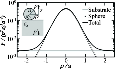
where z and ρ are axial and radial distances, respectively, from the dipole as shown in the inset of Fig. 1. The full-width at half-max (FWHM) of Fsphere versus ρ is FWHM=2z(21∕5−1)1∕2. If the dielectric sphere is resting on a substrate with permittivity εS, the first order contribution of the substrate to the force on the dipole may be estimated by calculating the force between the dipole and its image dipole in the substrate,15 whose magnitude is p′=p(εS−ε0)∕(εS+ε0). The force from the substrate without the sphere is then,
| (3) |
Figure 1 shows the total force on a dipole scanned in ρ at z=a, the dielectric constants are set to εP=εS=3.8ε0, that of fused silica.16
Figure 1.
Force on an electric dipole p as it is translated over a dielectric sphere. The dots indicate force from the sphere, the gray line indicates force from the substrate, and the black line indicates their sum. Inset: schematic of the model in which the dipole p rests a distance z above and ρ from the center of a dielectric sphere of radius a and dielectric permittivity εP. The sphere rests on a substrate of dielectric permittivity εM. An image dipole p′ is generated in the substrate. For the force calculation,z=a and all materials are silica, εP=εS=3.8ε0.
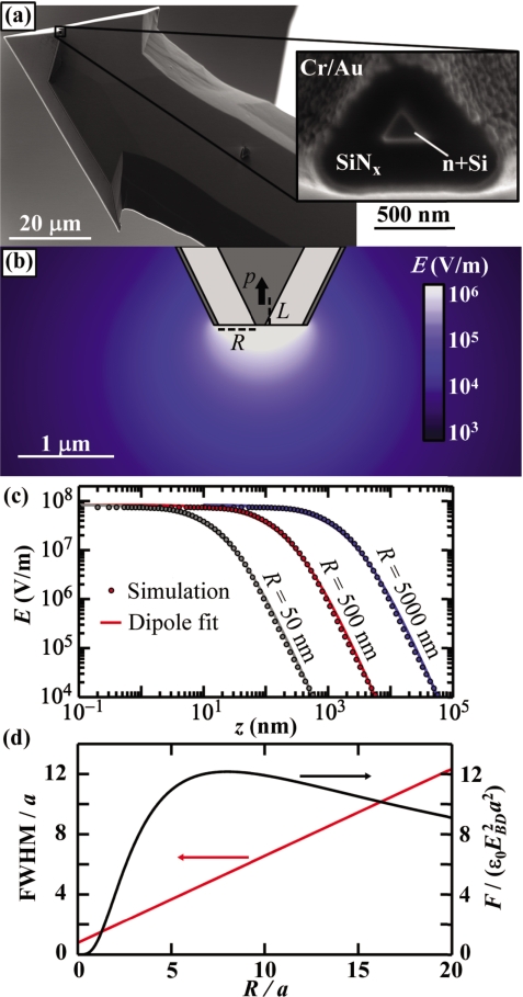
Coaxial probes such as the one shown in Fig. 2a create dipolar electric fields that are ideal for imaging with DEP. An axially symmetric finite element electrostatic simulation of the electric field profile of a coaxial probe is shown in Fig. 2b. In this simulation, a voltage V=1 V is applied to the inner conductor which is separated from a grounded shield by an insulating silicon nitride layer of thickness R=500 nm. Figure 2c shows the calculated axial electric field for a variety of tip sizes a distance z away from the end of the probe. The electric field of each probe is fit very well to the z-component of the dipolar electric field,
| (4) |
where L is the displacement of the dipole into the body of the probe as depicted in Fig. 2b. This fitting results in L≈0.75R and p≈26ε0VR2. Here, the electric field at the tip is chosen to be equal to the dielectric breakdown of microgaps in air EBD∼0.75 MV∕cm,17 imposing a maximum dipole strength for a given probe, p≈9.1ε0EBDR3. A tradeoff becomes evident, increasing the insulator thickness R increases the strength of the dipole but moves it further away from the sample. Figure 2d illustrates this tradeoff as the FWHM increases linearly with R while the maximum force increases to a maximum at R≈8a then decreases at larger R.
Figure 2.
(a) Scanning electron micrograph of a typical coaxial AFM probe with (inset) a zoomed in view of the coaxial tip. The inner n+silicon conductor is surrounded by ∼400 nm of low stress silicon nitride and a Cr/Au ground shield. (b) Axially symmetric finite element electrostatic simulation of electric field of a coaxial probe. The inner conductor is held at 1 V and the outer conductor is grounded. (c) Simulated axial electric field of three coaxial probes with varying insulator thickness R. The voltage of each is scaled to set the maximum electric field strength to the dielectric breakdown field EBD of air. Each field profile is fit to a dipolar electric field. (b) Resolution vs sensitivity of coaxial probes. Left axis: the FWHM of the force as measured from probes with varying R. Right axis: maximum force exerted on a coaxial probe by a dielectric sphere directly below the probe. The maxima at R≈8a indicates an optimal R to detect a given object.
Coaxial AFM probes [Fig. 2a] were fabricated by a previously described method.11 Cleaned AFM probes (Arrow-NC—Nanoword AG) were mounted on a metal carrier. Ohmic contacts are made to the probe by thermal evaporation of 15 nm of Ti and 100 nm of Al and annealing for 30 min at 325 °C in forming gas (20:1N2:H2). Probes are then coated in 500 nm of SiNx using chemical vapor deposition. Next, a 15 nm layer of Cr and a 30 nm layer of Au layer are deposited using thermal evaporation. The coaxial apertures are exposed using a focused ion beam. To create dielectric samples, a dilute suspension of 1±0.05 μm diameter silica beads (Polysciences, Inc.) is dried on a freshly cleaned silicon wafer that has a 300 nm layer of thermal oxide. The probes are mounted in an Asylum Research MFP-3D commercial AFM. The excitation voltage is created with a high voltage switchable power supply (BOP 500—Kepco Inc.). AFM measurements are performed in air at relative humidity below 20% to reduce the effects of adsorbed water.
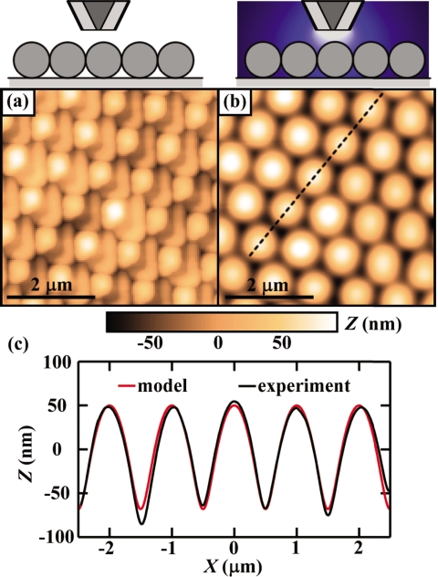
We demonstrate AFM imaging with DEP of a monolayer of silica microspheres. To image topographic features, we perform amplitude modulation AFM (AM-AFM) in which the tip is shaken near its resonance frequency and moved toward the sample until the oscillation amplitude decreases to a specified set point. Figure 3a shows a topographic image with no applied voltage. Under these conditions, the tip is intermittently striking the surface, which gives rise to imaging artifacts due to the similar size of the tip and features on the sample. In particular, the microspheres are difficult to discern because the pyramidal shape of the probe is visible. Figure 3b shows the same region imaged again with 50 Vrms applied to the probe at 5 kHz. The microspheres are now clearly visible and tip shape artifacts are gone. This is because DEP provides an attractive force strong enough such that the tip does not actually touch the surface, making this a noncontact imaging mode which allows the tip to be treated as a point dipole. It is important to note that the only difference in the imaging conditions is the addition of the voltage, the imaging conditions are otherwise identical. This approach provides a powerful approach for noncontact imaging of dielectric structures and materials.
Figure 3.
(a) Topographic image of a close packed monolayer of 1 μm diameter silica microspheres taken with a coaxial probe. Artifacts from the tip shape dominate the image. (b) Topographic image of the same region taken with 50 Vrms at 5 kHz applied to the inner conductor. Now the dielectrophoretic contribution dominates and the microspheres appear with high fidelity. (c) The black line is the line trace of (b) from the location shown with a dashed line. The lighter line is a fit of the dipole model showing good agreement.
A dipole model of the tip provides excellent agreement with topographical scans of the silica microspheres. We find agreement between a topographic line trace from Fig. 3b and a contour of constant force from the dipole model which demonstrates that we are imaging with DEP. The black line in Fig. 3c is a line cut from Fig. 3b across the peaks of the microspheres. We estimate the tip-sample force FTS in AM-AFM using a relationship valid in cases when the dominant interactions are conservative and only have significant values at the point of closest approach,18
| (5) |
where k is the effective spring constant, A0 is the free space amplitude, A is the damped oscillation amplitude, and Q is the mechanical quality factor of the cantilever. In our experiment, k=39 nN∕nm, A0=162 nm, A=88 nm, Q=534, predicting FTS≈2.9 nN. In order to independently estimate this force with our dipole model, we calculate the force on a dipole above a hexagonally close packed monolayer of beads with a=500 nm and εP=3.8ε0, resting on a substrate with εS=3.8ε0. We perform a least-squares fit contours of constant force to the experimental data with the best fit shown as a lighter line in Fig. 3c. The dipole model tracks the experimental data very well. Using a value for p≈4×10⁻²² Cm predicted from the maximum dipole scaling with R=400 nm, we find the best fit force to be FTS≈2.1 nN. The agreement between the force estimated by this method and the force estimated from the AM-AFM conditions shows that we are indeed imaging with DEP.
A comparison of DEP imaging with coaxial and unshielded probes illuminates the advantages of coaxial probes. An unshielded probe with tip radius Rtip is approximated by an electric monopole a distance Rtip above a sample3 while we have shown that a coaxial probe is well approximated by an electric dipole 0.75R above a sample. While imaging with DEP, both have spatial resolution comparable to the tip size, but the field of a dipole decays more quickly with distance so coaxial probes are less sensitive to distant features. By fabricating coaxial probes with smaller tips, it is possible to obtain superior spatial resolution than is possible with unshielded probes. The spatial resolution is given by the FWHM of Fsphere versus ρ while imaging a sphere of vanishing radius, a→0. Using the expressions above and the electric field of a monopole,14 we find unshielded probes have FWHM≈1.0Rtip while coaxial probes have FWHM≈0.6R.
We have shown that DEP may be used as a force contrast mechanism in AM-AFM and that coaxial AFM probes are well suited to image with this mechanism. This imaging technique is not limited to dielectric objects as conducting materials have large permittivities. Furthermore this method is well suited to study buried structures and structures with complex topography because of its noncontact method nature.
Acknowledgments
We thank Keith Jones at Asylum Research for helpful discussions, Jiangdong Deng for assistance with the AFM, and Jim MacArthur for help with electronics. We acknowledge support by the Department of Defense through a National Defense Science and Engineering Graduate (NDSEG) Fellowship, the National Cancer Institute MIT-Harvard Center of Cancer Nanotechnology Excellence, and the Department of Energy under Grant No. DE-FG02-07ER46422.
References
- Giessibl F. J., Rev. Mod. Phys. 75, 949 (2003). 10.1103/RevModPhys.75.949 [DOI] [Google Scholar]
- Oliver R. A., Rep. Prog. Phys. 71, 076501 (2008). 10.1088/0034-4885/71/7/076501 [DOI] [Google Scholar]
- Salmeron M., Oil Gas Sci. Technol. 56, 63 (2001). 10.2516/ogst:2001008 [DOI] [Google Scholar]
- Gramse G., Casuso I., Toset J., Fumagalli L., and Gomila G., Nanotechnology 20, 395702 (2009). 10.1088/0957-4484/20/39/395702 [DOI] [PubMed] [Google Scholar]
- Riedel C., Arinero R., Tordjeman P., Lévêque G., Schwartz G. A., Alegria A., and Colmenero J., Phys. Rev. E 81, 010801 (2010). 10.1103/PhysRevE.81.010801 [DOI] [PubMed] [Google Scholar]
- Crider P. S., Majewski M. R., Zhang J., Oukris H., and Israeloff N. E., Appl. Phys. Lett. 91, 013102 (2007). 10.1063/1.2753539 [DOI] [Google Scholar]
- Gao C. and Xiang X. -D., Rev. Sci. Instrum. 69, 3846 (1998). 10.1063/1.1149189 [DOI] [Google Scholar]
- Cho Y., Fujimoto K., Hiranaga Y., Wagatsuma Y., Onoe A., Terabe K., and Kitamura K., Appl. Phys. Lett. 81, 4401 (2002). 10.1063/1.1526916 [DOI] [Google Scholar]
- Hiranaga Y. and Cho Y., Rev. Sci. Instrum. 81, 023705 (2010). 10.1063/1.3274138 [DOI] [PubMed] [Google Scholar]
- Goto K. and Hane K., J. Appl. Phys. 84, 4043 (1998). 10.1063/1.368617 [DOI] [Google Scholar]
- Brown K. A., Aguilar J. A., and Westervelt R. M., Appl. Phys. Lett. 96, 123109 (2010). 10.1063/1.3372621 [DOI] [Google Scholar]
- Rosner B. T. and van der Weide D. W., Rev. Sci. Instrum. 73, 2505 (2002). 10.1063/1.1482150 [DOI] [Google Scholar]
- Voldman J., Annu. Rev. Biomed. Eng. 8, 425 (2006). 10.1146/annurev.bioeng.8.061505.095739 [DOI] [PubMed] [Google Scholar]
- Griffiths D. J., Introduction to Electrodynamics, 3rd ed. (Prentice Hall, New Jersey, 1999). [Google Scholar]
- Edmonds D. T., Eur. Biophys. J. 16, 255 (1988). 10.1007/BF00254060 [DOI] [Google Scholar]
- Gray D. E., American Institute of Physics Handbook, 3rd ed. (McGraw-Hill, New York, 1982), pp. 5–136. [Google Scholar]
- Wallash A. and Levit L., Proc. SPIE 4980, 87 (2003). 10.1117/12.478191 [DOI] [Google Scholar]
- García R. and Pérez R., Surf. Sci. Rep. 47, 197 (2002). 10.1016/S0167-5729(02)00077-8 [DOI] [Google Scholar]


