Abstract
This Letter describes how gold pyramidal nanoshells (nanopyramids) can be assembled into low- and high-order structures by varying the rate of solvent evaporation and surface wettability. Single-particle and individual-cluster dark field scattering spectra on isolated, dimers and trimers of nanopyramids were compared. We found that the short wavelength resonances blue-shifted as the particles assembled; the magnitude of this shift was greater for high-order structures. To test which assembled architecture supported a larger Raman-active volume, we compared their surface enhanced Raman scattering (SERS) response of the resonant Raman molecule methylene blue (λex = 633 nm). We discovered that high-order structures exhibited more Raman scattering compared to low-order assemblies. Finite-difference time-domain modeling of nanopyramid assemblies revealed that the highest electromagnetic field intensities were localized between adjacent particle faces, a result that was consistent with the SERS observations. Thus, the local spatial arrangement of the same number of nanoparticles in assembled clusters is an important design parameter for optimizing nanoparticle-based SERS sensors.
Keywords: Surface-enhanced Raman scattering (SERS), gold nanoparticles, nanopyramids, nanoparticle assembly, single particle dark field spectroscopy, finite-difference time-domain (FDTD) method
The assembly of nanoparticles (NPs) into hierarchical structures is a grand challenge in nanomaterials research because of the competition among forces involved, including entropy, electrostatics, and van der Waals. The relative contributions of these forces can be manipulated by tuning NP size,1 shape,2 medium of dispersion,3 and surface functionality.4–8 In addition, reducing the solvent evaporation rate has promoted the formation of nanoparticle assemblies.9 Most work in NP assembly has focused on generating two-dimensional (2D) or three-dimensional (3D) structures from spherical building blocks;10,11 however, the high symmetry of this particle shape limits the local structure of the assembled lattices. Recently, anisotropic nanoparticles have been used to form unique architectures such as 3D plasmonic crystals or gold nanorod superstructures.12–15 Control over the assembly of asymmetric NPs is important for applications in nanoelectronics, plasmonics, and photonics.16,17
NP assemblies are of considerable interest for surface-enhanced Raman spectroscopy (SERS) because closely spaced NP pairs produce intense, localized electromagnetic fields that act as SERS hot-spots.18 Most SERS investigations have focused on low-order assemblies, where the hot-spots are confined to a single region between two adjacent NPs.18–23 Alternatively, high-order assemblies can be constructed when particles are stacked within each other, such as nested pyramidal nanoshells, where all four flat faces of the two anisotropic particles were parallel and separated by a well-defined gap.24 These nested structures exhibited larger Raman scattering responses compared to single pyramidal nanoshells of the same gold thickness because of a larger SERS-active volume.24 Furthermore, particle shape offers a promising approach to investigate the effects of anisotropic assemblies in Raman scattering. Although Raman enhancement has been observed in NP dimers and unordered aggregates,18–23 a direct correlation between the overall shape of a hierarchical assembly and its SERS response has not been studied.
Here we compare the SERS response of low- and high-order assemblies of NPs using nanofabricated pyramidal nanoshells as a model system. First, the design rules for NP assembly were optimized by varying particle size, shell thickness, solvent evaporation rate, and surface wettability. We controlled the assembly of gold pyramidal nanoshells into two distinct configurations: low-order (side-to-side) and high-order (stacked) assemblies. Second, we measured their dark field (DF) scattering spectra and found that the short wavelength resonances blue-shifted as dimers were formed; the magnitude of this shift was greater for high-order dimers. When a third particle was stacked inside a high-order dimer to create a trimer, the spectral features of the high-order assembly were broadened; low-order trimers showed only a long wavelength peak. Finally, we found that high-order assemblies exhibited SERS responses greater than low-order assemblies. This observation was supported by finite-difference time-domain (FDTD) simulations, which revealed that stacked architectures exhibited a larger total volume of concentrated electric fields compared to side-to-side structures.
Figure 1 illustrates the two external conditions that are most important in assembling anisotropic particles on a surface: solvent evaporation rate and surface wettability. Pyramidal nanoshells were fabricated by Phase-shifting photolithography, Etching, E-beam, and Lift-off (PEEL),25 a procedure that can produce nanopyramids with variable base diameters (80 nm ≤ d ≤ 350 nm) and shell thicknesses (20 nm ≤ t ≤ 100 nm).26 For the assembly studies reported here, gold pyramids with d = 350 nm and variable t were investigated; the aqueous suspensions had a fixed concentration of ~20,000 particles/μL. When a 2-μL droplet of pyramid suspension was evaporated on a silicon substrate (contact angle θ = 34°, measured using a goniometer), the nanopyramids either tended to be isolated or formed aggregates at room temperature. To decrease the rate of water evaporation, we placed the substrates in sealed, double-rimmed Petri dishes, which reduced the rate from 6 μL/h to approximately 1.2 μL/h. When the sealed Petri dishes were placed in a refrigerator (4 °C), the rate of evaporation was slowed to ~0.08 μL/h. The evaporation rates were estimated by dispersing a known volume of pyramid solution on silicon and monitoring the time for the droplet to evaporate.
Figure 1.
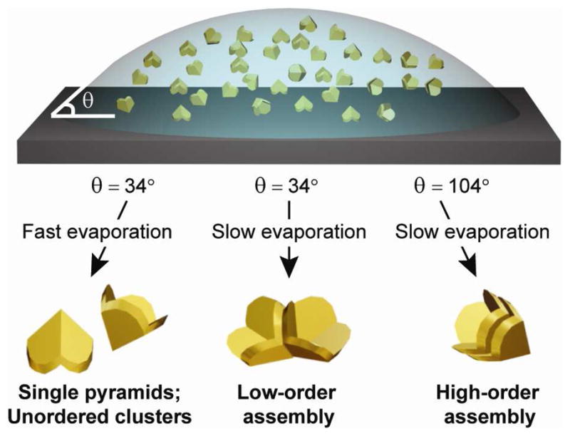
Scheme depicting the conditions required for achieving low- and high-order assemblies of pyramidal nanoshells.
Gold pyramidal nanoshells with 20- and 40-nm shell thicknesses tended to form more side-to-side assemblies compared to those with greater shell thicknesses (t = 60, 80, and 100 nm). This observation was likely because thicker pyramidal shells settled out of solution more rapidly than thinner ones. Under sealed and 4 °C-conditions, 70% of the 40 nm thick pyramids assembled in a side-to-side manner, 25% were unordered aggregates, and 5% remained isolated within the 2-mm2 droplet area. Of the side-to-side assemblies (Figs. 2a–2d), 50% were trimers, and the remainder consisted of dimers (35%) and tetramers (15%). Pyramids with smaller base diameters (d = 150 nm) and comparable shell thicknesses, however, did not form ordered assemblies.
Figure 2. Control over the assembly of pyramidal nanoshells.
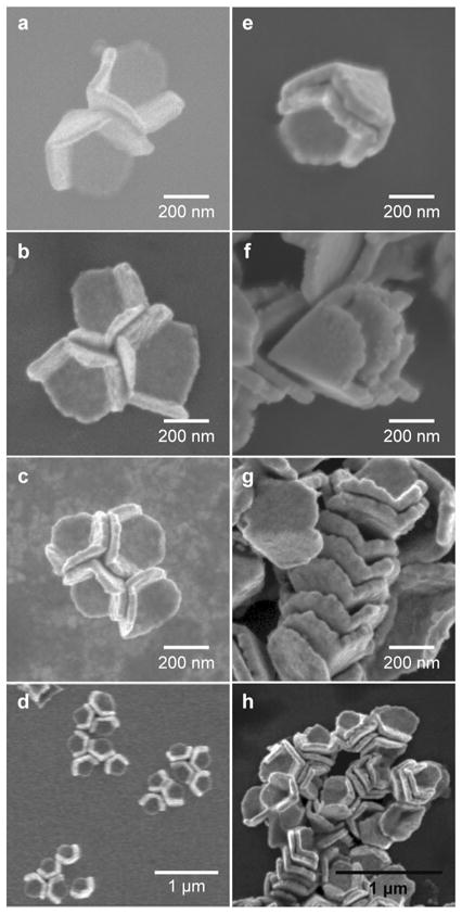
Scanning electron microscopy (SEM) images of the two types of assemblies in pyramidal nanoshells (t = 40 nm): (a–d) low-order and (e–h) high-order assemblies. (a) Side-by-side dimer (L2). (b) Side-by-side trimer (L3). (c) Side-by-side tetramer (L4). (d) Clusters of low-order assemblies. (e) Stacked dimer (H2). (f) Stacked trimer (H3). (g) Stacked assembly with seven particles. (h) Clusters of primarily high-order assemblies.
In order to assemble pyramidal nanoshells into stacks, we made the silicon surface hydrophobic (θ = 104°) by silanizing with tetrahydrooctyl trichlorosilane (5 h). Hence, for the same nanopyramid suspension volume, the droplet area in contact with the substrate was smaller, and the particle density was therefore higher throughout the droplet area.3 When a suspension of pyramidal nanoshells was drop-cast and evaporated in sealed Petri dishes on hydrophobic substrates, 20% of the particles assembled into stacks (Figs. 2e–2h), and 80% formed unordered aggregates. To increase the total number of pyramidal nanoshell stacks, we reduced the rate of evaporation to 0.03 μL/hr (4 °C). Although both low-and high-level order were observed under these conditions, high-order assembly was prevalent (Figs. 2e–2f): approximately 60% of pyramids assembled in high-order stacks, 5% in low-order assemblies, and the remainder exhibited no order. Both the density of stacks and aggregates were most dense along the edge of the evaporated droplet, although assembly occurred throughout the entire area. The maximum number of pyramids we observed in a single stack was seven (Fig. 2g). Pyramidal depositions on surfaces with intermediate wettabilities (θ = 41°, 76°, and 94°) showed that both the number of pyramidal stacks and the number of particles within a stack increased with surface hydrophobicity. Besides assemblies with either low- or high-order exclusively, some structures were composed of small (2–4) stacks within side-to-side assemblies (Fig. 2h).
The assembly of pyramidal nanoshells into low- and high-order structures provides a unique platform to investigate the SERS response of NPs organized into different architectures. To correlate the particle orientation determined by SEM images with the DF scattering and Raman scattering spectra, we first patterned transparent ITO (n = 1.8) substrates with Au alignment markers and then assembled 25-nm thick Au nanopyramidal shells (Supporting Information). Figure 3 depicts Raman scattering images and spectra (excitation wavelength λex = 633 nm, He-Ne laser) and DF scattering spectra of low- and high-order dimers, L2 and H2, compared to an isolated tip-down (TD) nanopyramid. The DF scattering spectra revealed that the assembly of two pyramids into a dimer not only increased the overall scattering intensity, but also blue-shifted the short wavelength resonances. The 720-nm peak in TD was shifted to ~640 nm for H2 and ~690 nm for L2 (Fig. 3b). Also, an additional resonance appeared at longer wavelengths; the two resonances were located further apart for H2 (Δλ = 170 nm) versus L2 (Δλ = 70 nm). The higher optical scattering of H2 at λex may lead to greater Raman scattering intensity compared to that from L2.
Figure 3. Correlation of the DF scattering and SERS response of single nanopyramids and dimers.
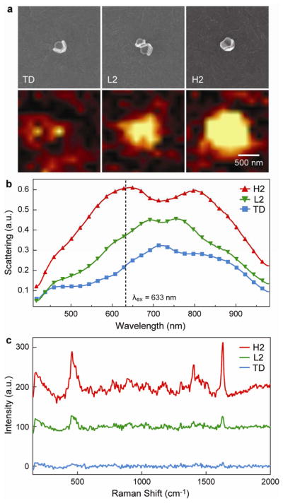
(a) (top) SEM and (bottom) corresponding Raman images of the 1621–1624 cm−1 MB vibrational mode intensity from a single tip-down pyramid (TD), a low-order dimer of pyramidal nanoshells (L2), and a high-order dimer of pyramidal nanoshells (H2). The scale bar applies to all images. (b) DF scattering spectra of TD, L2, and H2. (c) Raman spectra corresponding to the most intense point of the Raman image in (a).
A direct comparison of the Raman scattering from the two different assemblies is crucial to develop optimized SERS substrates based on NPs. Raman spectra and images were recorded with a confocal Raman microscope (Alpha, WiTec Instruments) equipped with a piezo scanner and 100× microscope objective (NA = 0.90, Nikon). The nanopyramidal assemblies were functionalized with methylene blue (MB) and excited at λex = 633 nm. We obtained Raman images (2 μm × 2 μm) by mapping the Raman intensity integrated over 1590–1660 cm−1; Fig. 3a (bottom) represents a map of the 1624 cm−1 vibrational mode. The signal maps collected from the images were set to the same color scale (low = −15, high = 150) so that the SERS intensity from the different assembled structures could be compared directly. As expected, Fig. 3c shows that the SERS response from the assembled nanopyramid dimers was greater than that from two isolated tip-down pyramids, an effect that was also predicted for Ag triangles.27 The order of pyramid assembly strongly affected the scattered intensity of the 1624 cm−1 mode, where the Raman scattering from H2 was 4.5 times higher than that from L2.
The superior SERS performance of high-order structures compared to low-order assemblies can, in part, be explained by considering the electromagnetic field distribution at λex = 633 nm. Figure 4 shows x-z cross sections of the electric field intensity modeled using the FDTD method (Supporting Information). The separations between the nanopyramids in L2 (15 nm) and H2 (28 nm) were determined by analyzing SEM images (Supporting Information). The locations of highest field intensity were found at the edges of the nanopyramidal shell and between the parallel faces of adjacent particles; other separations did not confine the fields as efficiently (Supporting Information). The four aligned faces of H2 (or four face-face pairs) resulted in a significantly larger region of high electric field intensity compared to L2, which has only one face-face pair. Hence, the larger SERS signal from stacked pyramidal nanoshells versus side-to-side assemblies may be attributed to an increased Raman-active volume. The larger distance between H2 stacks compared to L2 side-to-side assemblies may also influence the magnitude of the electric field intensity and SERS signal.28
Figure 4. FDTD simulation of the electromagnetic field intensity distribution for single particles and dimers at λ = 633 nm.
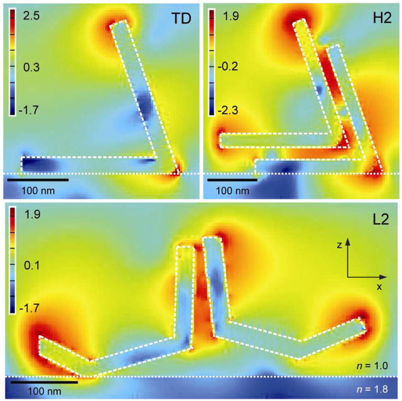
|Ez|2 was calculated for a single TD and dimers H2 and L2. Cross-sections were taken along the central axis in the x-z plane intersecting the tips of TD and H2. For L2, the electric-field intensity was measured in the x-z plane along the long axis of the dimer, where the gap separating the two pyramids was oriented perpendicular to the plane of the detector. The intensities are plotted on a logarithmic scale.
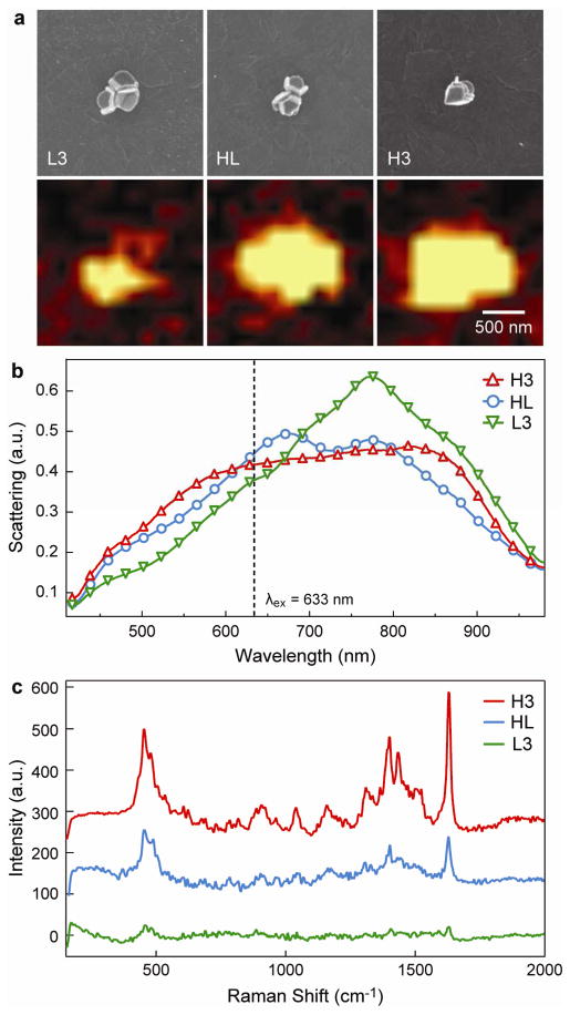
To understand the properties of assemblies ordered to greater extents, we characterized nanopyramid trimers (Fig. 5). DF scattering measurements showed that the addition of a third pyramid in a side-to-side orientation (L3) resulted in a single peak at 780 nm (Fig. 5b); this change in spectrum compared to TD (Fig. 3b) may result from the larger size of the structure. When the third pyramid was stacked within one of the two side-to-side pyramids (HL), the spectral features were very similar to those of a side-to-side dimer. The stacking of a pyramid within a high-order dimer to form H3 did not cause any resonance to shift, although these features were broadened. At λex = 633 nm, the optical scattering intensities of HL and H3 were 1.5 and 1.4 times as great as L3, respectively. The Raman scattering of nanopyramid trimers followed trends similar to those of the dimers except for L3 (Fig. 5c). In the case of L3, the intensity of the SERS signal was nearly equivalent to that of three isolated pyramids, which may be attributed to the reduced scattering of L3 at the Raman excitation wavelength. For HL and H3, the signal was 2.5 and 10 times higher than that from three isolated particles. These observations also confirm that high-order structures yield increased SERS signals compared to low-order assemblies.
Figure 5. Correlation of the DF scattering and SERS response of low-, mixed-, and high-order trimers.
(a) (top) SEM and (bottom) corresponding Raman images of the 1621–1624 cm−1 MB vibrational mode intensity from a low-order trimer (L3), mixed-order assembly of three particles (HL), and high-order trimer (H3). The scale bar applies to all images. (b) DF scattering spectra of L3, HL, and H3. (c) Raman spectra corresponding to the most intense point of the Raman image in (a).
In summary, we have controlled the assembly of anisotropic pyramidal nanoshells into two unique geometries by varying the rate of solvent evaporation and the wettability of the surface. These distinct architectures offer a route to the rational design of NP assemblies for SERS applications. An explanation for the increased Raman scattering by high-order assemblies was investigated using FDTD calculations, which indicated that the electromagnetic field was confined within the gapped regions between parallel nanopyramid faces. Hence, measurements and modeling suggest that high-order assemblies are more promising than low-order assemblies as SERS substrates because they support a larger geometric region of high electric field intensity, or a larger Raman-active volume. We anticipate that these findings will provide additional guidance in developing SERS-based chemical and biological sensors.
Supplementary Material
Acknowledgments
This work was supported in part by the MRSEC program of the National Science Foundation (DMR-0520513) at the Materials Research Center of Northwestern University, the NSF NSEC program at Northwestern University (EEC-0647560), the David and Lucile Packard Foundation, and the NIH Director’s Pioneer Award (DP1OD003899). This work used the NUANCE Center facilities, which are supported by NSF-MRSEC, NSF-NSEC and the Keck Foundation. We thank the Mirkin group, especially M. L. Pedano, for assistance with the confocal Raman microscope, and thank J.Y. Suh for help with FDTD modeling.
References
- 1.Talapin DV. Lego Materials. ACS Nano. 2008;2:1097–1100. doi: 10.1021/nn8003179. [DOI] [PubMed] [Google Scholar]
- 2.Jana NR. Shape Effect in Nanoparticle Self-Assembly. Angew Chem, Int Ed. 2004;43:1536–1540. doi: 10.1002/anie.200352260. [DOI] [PubMed] [Google Scholar]
- 3.Cai Y, Newby BZ. Marangoni Flow-Induced Self-Assembly of Hexagonal and Stripelike Nanoparticle Patterns. J Am Chem Soc. 2008;130:6076–6077. doi: 10.1021/ja801438u. [DOI] [PubMed] [Google Scholar]
- 4.Polayarapu L, Xu Q. Water-soluble Conjugated Polymer-induced Self-Assembly of Gold Nanoparticles and its Application to SERS. Langmuir. 2008;24:10608–10611. doi: 10.1021/la802319c. [DOI] [PubMed] [Google Scholar]
- 5.Park SY, Lytton-Jean AKR, Lee B, Weigand S, Schatz GC, Mirkin CA. DNA-Programmable Nanoparticle Crystallization. Nature. 2008;451:553–556. doi: 10.1038/nature06508. [DOI] [PubMed] [Google Scholar]
- 6.Nykypanchuk D, Maye MM, van der Lelie D, Gang O. DNA-Guided Crystallization of Colloidal Nanoparticles. Nature. 2008;451:549–552. doi: 10.1038/nature06560. [DOI] [PubMed] [Google Scholar]
- 7.Shevchenko EV, Talapin DV, Kotov NA, O’Brien S, Murray CB. Structural Diversity in Binary Nanoparticle Superlattices. Nature. 2006;439:55–58. doi: 10.1038/nature04414. [DOI] [PubMed] [Google Scholar]
- 8.Min YAM, Kristiansen K, Golan Y, Israelachvili J. The Role of Interparticle and External Forces in Nanoparticle Assembly. Nat Mater. 2008;7:527. doi: 10.1038/nmat2206. [DOI] [PubMed] [Google Scholar]
- 9.Brinker CJ. Evaporation-Induced Self-Assembly: Functional Nanostructures Made Easy. Mater Res Bull. 2004;29:631–640. [Google Scholar]
- 10.Collier CP, Vossmeyer T, Heath JR. Nanocrystal Superlattices. Annu Rev Phys Chem. 1998;49:371–404. doi: 10.1146/annurev.physchem.49.1.371. [DOI] [PubMed] [Google Scholar]
- 11.Pileni MP. Nanocrystal Self-Assemblies: Fabrication and Collective Properties. J Phys Chem B. 2001;105:3358–3371. [Google Scholar]
- 12.Guerrero-Martinez A, Perez-Juste J, Carbo-Argibay E, Tardajos G, Liz-Marzan LM. Gemini-Surfactant-Directed Self-Assembly of Monodisperse Gold Nanorods into Standing Superlattices. Angew Chem Int Ed. 2009;48:1–6. doi: 10.1002/anie.200904118. [DOI] [PubMed] [Google Scholar]
- 13.Tao AR, Ceperley DP, Sinsermsuksakul P, Neureuther AR, Yang P. Self-Organized Silver Nanoparticles for Three-Dimensional Plasmonic Crystals. Nano Lett. 2008;8:4033–4038. doi: 10.1021/nl802877h. [DOI] [PubMed] [Google Scholar]
- 14.Ryan KM, Mastroianni A, Stancil KA, Liu HT, Alivisatos AP. Electric-Field-Assisted Assembly of Perpendicularly Oriented Nanorod Superlattices. Nano Lett. 2006;6:1479–1482. doi: 10.1021/nl060866o. [DOI] [PubMed] [Google Scholar]
- 15.Khanal BP, Zubarev ER. Rings of Nanorods. Angew Chem Int Ed. 2007;46:2195–2198. doi: 10.1002/anie.200604889. [DOI] [PubMed] [Google Scholar]
- 16.Fendler JH. Nanoparticles and Nanostructured Films. Wiley-VCH; Weinhein: 1998. [Google Scholar]
- 17.Rycenga M, McLellan JM, Xia Y. Controlling the Assembly of Silver Nanocubes through Selective Functionalization of their Faces. Adv Mater. 2008;20:2416–2420. [Google Scholar]
- 18.Klajn R, Wesson PJ, Bishop KJM, Grzybowski BA. Writing Self-Erasing Images using Metastable Nanoparticle “Inks”. Angew Chem, Int Ed. 2009;48:1–6. doi: 10.1002/anie.200901119. [DOI] [PubMed] [Google Scholar]
- 19.Nie S, Emory SR. Single-molecule Detection and Spectroscopy by Surface-Enhanced Raman Scattering. Science. 1997;275:1102–6. doi: 10.1126/science.275.5303.1102. [DOI] [PubMed] [Google Scholar]
- 20.Jiang J, Bosnick K, Maillard M, Brus L. Single Molecule Raman Spectroscopy at the Junctions of Large Ag Nanocrystals. J Phys Chem B. 2003;107:9964–9972. [Google Scholar]
- 21.Camden JP, Dieringer JA, Wang YM, Masiello DJ, Marks LD, Schatz GC, Van Duyne RP. Probing the Structure of Single-Molecule Surface-enhanced Raman Scattering Hot Spots. J Am Chem Soc. 2008;130:12616–12617. doi: 10.1021/ja8051427. [DOI] [PubMed] [Google Scholar]
- 22.Li WY, Camargo PHC, Lu XM, Xia YN. Dimers of Silver Nanospheres: Facile Synthesis and Their Use as Hot Spots for Surface-Enhanced Raman Scattering. Nano Lett. 2009;9:485–490. doi: 10.1021/nl803621x. [DOI] [PMC free article] [PubMed] [Google Scholar]
- 23.Fromm DP, Sundaramurthy A, Kinkhabwala A, Schuck PJ, Kino GS, Moerner WE. Exploring the Chemical Enhancement for Surface-enhanced Raman Scattering with Au Bowtie Nanoantennas. J Chem Phys. 2006;124:061101. doi: 10.1063/1.2167649. [DOI] [PMC free article] [PubMed] [Google Scholar]
- 24.Lin JY, Hasan W, Yang J-C, Odom TW. Optical Properties of Nested Pyramidal Nanoshells. J Phys Chem C ASAP. doi: 10.1021/jp910627r. [DOI] [PMC free article] [PubMed] [Google Scholar]
- 25.Henzie J, Kwak ES, Odom TW. Mesoscale Metallic Pyramids with Nanoscale Tips. Nano Lett. 2005;5:1199–1202. doi: 10.1021/nl0506148. [DOI] [PubMed] [Google Scholar]
- 26.Lee J, Hasan W, Stender CL, Odom TW. Pyramids: A Platform for Designing Multifunctional Plasmonic Particles. Acc Chem Res. 2008;41:1762–1771. doi: 10.1021/ar800126p. [DOI] [PubMed] [Google Scholar]
- 27.Hao E, Schatz GC. Electromagnetic Fields around Silver Nanoparticles and Dimers. J Chem Phys. 2004;120:357–366. doi: 10.1063/1.1629280. [DOI] [PubMed] [Google Scholar]
- 28.Qin LD, Zou SL, Xue C, Atkinson A, Schatz GC, Mirkin CA. Designing, Fabricating, and Imaging Raman Hot Spots. Proc Natl Acad Sci U S A. 2006;103:13300–13303. doi: 10.1073/pnas.0605889103. [DOI] [PMC free article] [PubMed] [Google Scholar]
Associated Data
This section collects any data citations, data availability statements, or supplementary materials included in this article.


