

1. Introduction
Coinage metals, such as Au, Ag, and Cu, have been important materials throughout history.1 While in ancient cultures they were admired primarily for their ability to reflect light, their applications have become far more sophisticated with our increased understanding and control of the atomic world. Today, these metals are widely used in electronics, catalysis, and as structural materials, but when they are fashioned into structures with nanometer-sized dimensions, they also become enablers for a completely different set of applications that involve light. These new applications go far beyond merely reflecting light, and have renewed our interest in maneuvering the interactions between metals and light in a field known as plasmonics.2–6
In plasmonics, the metal nanostructures can serve as antennas to convert light into localized electric fields (E-fields) or as waveguides to route light to desired locations with nanometer precision. These applications are made possible through a strong interaction between incident light and free electrons in the nanostructures. With a tight control over the nanostructures in terms of size and shape, light can be effectively manipulated and controlled with unprecedented accuracy.3,7 While many new technologies stand to be realized from plasmonics, with notable examples including superlenses,8 invisible cloaks,9 and quantum computing,10,11 conventional technologies like microprocessors and photovoltaic devices could also be made significantly faster and more efficient with the integration of plasmonic nanostructures.12–15 Of the metals, Ag has probably played the most important role in the development of plasmonics, and its unique properties make it well-suited for most of the next-generation plasmonic technologies.16–18
1.1. What is Plasmonics?
Plasmonics is related to the localization, guiding, and manipulation of electromagnetic waves beyond the diffraction limit and down to the nanometer length scale.4,6 The key component of plasmonics is a metal, because it supports surface plasmon polariton modes (indicated as surface plasmons or SPs throughout this review), which are electromagnetic waves coupled to the collective oscillations of free electrons in the metal.
While there are a rich variety of plasmonic metal nanostructures, they can be differentiated based on the plasmonic modes they support: localized surface plasmons (LSPs) or propagating surface plasmons (PSPs).5,19 In LSPs, the time-varying electric field associated with the light (Eo) exerts a force on the gas of negatively charged electrons in the conduction band of the metal and drives them to oscillate collectively. At a certain excitation frequency (w), this oscillation will be in resonance with the incident light, resulting in a strong oscillation of the surface electrons, commonly known as a localized surface plasmon resonance (LSPR) mode.20 This phenomenon is illustrated in Figure 1A. Structures that support LSPRs experience a uniform Eo when excited by light as their dimensions are much smaller than the wavelength of the light.
Figure 1.

Schematic illustration of the two types of plasmonic nanostructures discussed in this article as excited by the electric field (Eo) of incident light with wavevector (k). In (A) the nanostructure is smaller than the wavelength of light and the free electrons can be displaced from the lattice of positive ions (consisting of nuclei and core electrons) and collectively oscillate in resonance with the light. This is known as a localized surface plasmon resonance (LSPR). In (B) the nanostructure has one dimension much larger than the wavelength of light. In this case, light coupled to the nanostructure will excite the free electrons to create a propagating surface plasmon (PSP) that can travel along the surface of the metal nanostructure.
In contrast, PSPs are supported by structures that have at least one dimension that approaches the excitation wavelength, as shown in Figure 1B.4 In this case, the Eo is not uniform across the structure and other effects must be considered. In such a structure, like a nanowire for example, SPs propagate back and forth between the ends of the structure. This can be described as a Fabry-Perot resonator with resonance condition l=nλsp, where l is the length of the nanowire, n is an integer, and λsp is the wavelength of the PSP mode.21,22 Reflection from the ends of the structure must also be considered, which can change the phase and resonant length. Propagation lengths can be in the tens of micrometers (for nanowires) and the PSP waves can be manipulated by controlling the geometrical parameters of the structure.23
1.2. Plasmonics in Nanoscience and Nanotechnology
In the past the ability to focus light was solely in the realm of dielectric materials. These materials, however, cannot localize light to areas smaller than half a wavelength of light (λ/2) or confine electromagnetic modes to volumes less than (λ/2)3. In contrast, surface plasmon modes are primarily limited by the size of the plasmonic structure that supports them: a nanostructure can thereby focus and guide light down to the nanometer regime. By tailoring the size, shape, and environment of a metal nanostructure, light can be manipulated in many unique ways.24,25 It is no surprise that recent advances in the preparation and assembly of metal nanostructures have opened new doors to precise manipulation/control of light, and consequently to applications that were previously considered impossible.2
As an optical phenomenon, SP has been known for more than 150 years, with the first demonstration being documented by Michael Faraday in 1857.26 Its connection with nanoscale science and technology was not widely or actively explored until recently.27 Plasmonics is part of nanotechnology because nanostructures are used i) as active components to focus, guide, and manipulate light, and ii) as building blocks for larger, more complex “metamaterials” sought for controlling light. While the interaction of light and metal nanoparticles has long attracted interest of scientists, plasmonics represents a relatively new level of control and study involving both nanostructures and light. In contrast to simply establishing the valuable optical properties of metal nanostructures, this interaction is now controlled for a specific purpose to manipulate the propagation of light. Plasmonics is also a burgeoning field of nanoscience because sophisticated models, theories, and methods are being developed to understand the interaction between a metal nanostructure and light.3,7
Plasmonics is also different from many past applications and studies of nanoparticles that rely on the material properties of the nanostructure or its small size. These non-plasmonic applications include, for example, electron confinement,28 electron tunneling,29 ballistic transport,30 and superparamagnetism.31 In contrast to these applications, plasmonics requires a coupling between an electromagnetic wave and the metal nanostructure to generate a surface plasmon. Without incident light, the structure does not have a plasmonic function. More importantly, plasmonics is unique in that it can use nanostructures of many different sizes (tens to hundreds of nanometers) and thus bridge the gap between the micrometer and nanometer levels. This is best seen in the example of Ag nanowires, which can guide light at deep-subwavelength scales over micrometer distances.23 Plasmonics is therefore a new subfield of nanoscale science and technology that aims to understand and control light using metal nanostructures in novel ways.
1.3. What is Unique about Silver?
Silver is probably the most important material in plasmonics. It offers many advantages over Au, Cu, Li, and Al – other metals known to support SPs in the visible (vis) and near-infrared regions (NIR).16,32 In terms of plasmonics, it is important to choose a metal that can support a strong SP at the desired resonance wavelength.5,33 Silver is able to do so across the spectrum from 300 to 1200 nm. The ability of a metal nanoparticle to support an SP is dependent on its dielectric function ε, which includes real part (εr) and imaginary part (εi) and both vary with excitation wavelength (λ). The dielectric function of a material reflects the unique interaction between its electrons and the light.
The simplest way to describe LSPR can be found in Mie theory for calculating the extinction (absorption + scattering) cross section of a metal nanosphere:34
| (1) |
where Cext is the extinction cross section, R is the radius, and εm is the relative dielectric constant of the medium surrounding the nanosphere. This equation shows that the interaction between a metal nanoparticle and light depends strongly on its dielectric properties (εr and εi). While other factors are also important, from an engineering perspective the material properties of the plasmonic structure are the key, as the environment and other parameters (like excitation wavelength) are often fixed. When the denominator of the bracketed expression in Equation (1) approaches zero, Cext will become extremely large and the optical absorption and scattering at this particular frequency would also be exceedingly strong. This is known as a resonance condition. In order to achieve this, εr must be close to −2εm, which is not possible for standard dielectrics and non-metals that typically have εr values between 1 and 50.35 Figure 2 plots εr and εi for Ag, Au and Si, showing that Si has large positive values for εr, similar to other non-metal materials. Equation (1) also indicates that εi should be close to zero in order to support a strong resonance, a condition that can only be satisfied by some of the metals.36 In general, no LSP or PSP sufficiently strong for plasmonic applications can be formed without a negative εr, and large εi values mean a lossier or weaker plasmon. The SP strength (or damping) can be described using the quality factor (Q):32
| (2) |
Figure 2.

A plot of the (A) real, εr, and (B) imaginary, εi, components of the dielectric function of Ag, Au, and Si as a function of wavelength.
The SP strength is directly proportional to Q, and large values of Q mean strong plasmons (both LSPs and PSPs) and small values indicate a lossy or weak SP with a a small Cext. In general, Q should be larger than ~10 for most plasmonic applications. The quality factors for a number of metals are plotted in Figure 3. Obviously, Ag has the largest quality factor across most of the spectrum from 300 to 1200 nm. In contrast, Al is only suitable for applications in the ultraviolet (UV) region. Interband transitions, where electrons are excited from the conduction band to higher energy levels, also play an important role in dampening the SP modes.37 Typically, these transitions take place at much higher frequencies than the LSPRs, as in the case of Ag. For Au and Cu, however, these transitions limit their LSPR excitation to wavelengths longer than 500 and 600 nm, respectively.38
Figure 3.

The quality factor (Q) of the LSPR for a metal/air interface. A higher Q denotes less damping and a stronger plasmon resonance. The shaded area represents the region of interest to many plasmonic applications. Reproduced with permission from [32]. Copyright 2009 Elsevier.
In practical applications, the material properties of metals may out-weigh their differences in plasmonic properties. Based on the quality factor, Li should be a candidate as good as Au and Cu in supporting surface plasmons. However, this metal is so reactive and hard to handle that it is seldom considered and explored for plasmonic applications. Historically, Ag has been known for its widespread use in photography and staining of biological tissues due to the black color associated with the large aggregates of Ag nanoparticles.39 Silver also has the highest electrical and thermal conductivity among all metals, making it an ideal component for electrical interconnection. When exposed to air, Ag is not oxidized, but forms a silver sulfide film on its surface, which should be more or less transparent to the visible light.40,41 This thin film of silver sulfide can form in one day and, over a month, can become 60 Å in thickness for thin films of silver. It is worth pointing out that the black coating commonly observed on the surface of silverware is due to sulfuration with the sulfur in air,42 not oxidation.
As a disadvantage, Ag nanostructures (or more appropriately, Ag+ ions coming off from the nanostructures) are considered to be toxic, although passivating the surface can greatly increase their stability and thus attenuate or eliminate their toxicity.43 Instability and toxicity are also two major concerns for Cu, especially for the nanoscale structures. In contrast, Au is well-known for its bio-inertness, and its surface is believed to be oxide free. For these reasons, Au nanostructures are well-suited for in vivo applications with humans.44 In contrast, Ag nanostructures are largely used in plasmonic applications outside a human body (e.g., plasmonic antennas and circuits for concentrating and guiding light), where they have consistently reported much better performance than Au-based nanostructures.45–48
The difficulty of fabricating nanostructures, and thier cost, will also determine the usefulness of a metal for plasmonic applications, especially for large-scale applications. As shown in Table 1, the cost varies dramatically across the metals from ~$1,207 (per ounce) for Pt to ~$0.049 for Al. Silver is relatively cheap (~$13.4) among the metals that support plasmons. While both Al and Cu are cheaper, they have limitation in terms of the plasmons they can support, as discussed above. More importantly is the precedent and ease with which these metals can be prepared as nanostructures with controllable sizes and shapes. Over the past decade, Au, Ag, and Pd have all been prepared in a large variety of nanostructures using chemical methods.49 Taking into account the unsuitability of Pd for plasmonic applications, Au and Ag are the most promising, and indeed the most widely used materials in plasmonics. Gold is, however, almost 50 times more expensive than Ag is. While the application and scale of production will ultimately decide which metal is the best, Ag compared with the other metals is unique for its excellent qualities in terms of plasmonic ability, available nanostructures, and material cost.
Table 1.
Comparison of the suitability of different metals for plasmonic applications.
| Metal | Plasmonic Ability | Stability | Nanostructure Formation |
Cost (per ounce) |
|---|---|---|---|---|
| Aluminum (Al) | Good in UV region | Stable after surface passivation | Very few nanostructures; used in lithographic patterning | $0.049 |
| Copper (Cu) | Interband transisitons below 600 nm | Easy oxidation | Very few nanostructures | $14.8 |
| Gold (Au) | Interband transistions below 500nm; High quality factor | Very stable; biocompatible | Many nanostructures | $950 |
| Palladium (Pd) | Low quality factor; Not suitable for plasmonics | Stable | Many nanostructures | $265 |
| Platinum (Pt) | Low quality factor; Not suitable for plasmonics | Stable | Many nanostructures | $1,207 |
| Silver (Ag) | Highest in quality factor | Oxidation; biocompatibilty issues | Many nanostructures | $13.4 |
1.4. Scope and Organization of the Review
This review discusses a variety of Ag nanostructures prepared via solution-phase methods, with a minimal discussion of lithographic approaches in the context of their use in fabricating plasmonic nanostructures. It mainly focuses on both LSPRs and PSPs on nanostructures (not thin films). This review also discusses how engineering the physical properties (size, shape, etc), environment, and assembly of Ag nanostructures can affect their ability to support SPs and their potential for plasmonic applications. It emphasizes advancements made over the past five years (2004–2009), and while examples specific to Ag nanostructures are highlighted, fundamental studies using Au nanostructures are also cited for comparison or completeness. The objectives of this review are: i) to review the chemical methods used for generating Ag nanostructures; ii) to illustrate how light can be controlled by Ag nanostructures through SP coupling; iii) to discuss the limits and unknown variables associated with understanding and control of SPs with Ag nanostructures and; iv) to sketch some of the interesting applications and research directions involving Ag nanostructures.
2. Preparation of Silver Nanostructures
2.1. Chemical Synthesis
The size and shape of nanostructures define and control their unique plasmonic properties. The ability to make Ag nanostructures with well-controlled morphologies makes it possible to study the plasmonic phenomenon discussed in Section 4. At present, a wealth of methods are available for generating Ag nanostructures with different sizes and shapes.50–52 Table 2 provides an overview of the many structures that have been synthesized in the solution phase. Here, we will focus our discussion on synthetic approaches that primarily use chemical reduction to generate elemental Ag from a precursor and consequently generate Ag nanostructures. When a Ag precursor is mixed with a reducing agent and a colloidal stabilizer under appropriate conditions, we are able to generate Ag nanostructures with different sizes and shapes. In past studies, AgNO3 was the most commonly used precursor but our most recent work demonstrates that CF3COOAg may be a better choice because it has a lower reaction temperature, it eliminates NO2 dervided from the decompostion of NO3−, it is insensitive to trace impurities from the solvent (ethylene glycol), and it allows the reaction to be scaled up.53 Chemical reducing agents, such as sodium borohydride, alcohols, and sodium citrate, are typically used to reduce the dissolved Ag+ ions to Ag atoms which grow into small clusters and eventually nanostructures.54–56 Polymers and surfactants are used to stabilize the nanostructures during and after formation, and in some cases, they can also play the role to direct particle growth to the desired shapes.
Table 2.
A summary of the shapes, LSPR absorption peaks, demonstrated applications, and methods for synthesis of Ag nanostructures discussed in this review.
The red lines in the illustration refer to a crystalline plane and the dark faces are {100} and the light faces are {111}.
| Shape | Illustration | LSRBa | Applicationsb | Method of Synthesis | Ref# |
|---|---|---|---|---|---|
| Sphere and quasi-sphere | 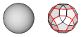 |
320 – 450 | SERS; LSPR sensing assembly | Polyol process (single-crystal); Citrate reduction (quasi-sphere) | 58, 85, 94, 330, 358 |
| Cube and truncated cube |  |
400 – 480 | SERS; LSPR sensing assembly | Polyol process; Seed-mediated growth | 53, 80, 96, 200, 214, 371 |
| Tetrahedron and truncated tetrahedron | 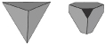 |
350 – 450 | SERS | Polyol process; Light-mediated growth | 113 |
| Octahedron and truncated octahedron | 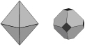 |
400 – 500 | Assembly | Polyol process; seed-mediated growth; light-mediated growth | 105, 334, 346, 364 |
| Bar | 350 – 900 | SERS | Polyol process | 93 | |
| Spheriod | 350 – 900 | SERS | Polyol process | 93, 529 | |
| Right bipyramid |  |
500 – 700 | - | Polyol process | 81, 112 |
| Beam | - | Electron transport | Polyol process | 73 | |
| Decahedron |  |
350 – 450 | - | Seed-mediated growth; light-mediated growth; citrate reduction | 101 |
| Wire and rod | 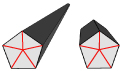 |
380 – 460 | Wave guiding electronics; SERS; assembly | Seed-mediated growth | 17, 47, 63, 83, 98, 99, 100, 222, 244, 256, 329, 357 |
| Polygonal plates and disc |  |
350 – 1000 | SERS; LSPR sensing | Light-mediated growth; polyol process | 18, 92, 111, 123, 126, 134, 183 |
| Branched structures |  |
400 – 1100 | SERS | Seed-mediated growth | 251 |
| Hollow structures |  |
380 – 800 | SERS; LSPR sensing | Template-directed growth | 131, 137, 146, 192, 262 |
The main absorption peak (nm).
Assembly means the nanostructure has been assembled into larger structures for plasmonic applications or studies.
2.1.1. Citrate Reduction
Lee and Meisel first reported the synthesis of Ag colloids by reducing AgNO3 with citrate in an aqueous solution in 1982.57 This method remains a popular approach to quickly generating Ag colloids as it does not require extensive synthetic skills.58–60 In a typical synthesis, Ag nanoparticles are obtained by adding a set amount of aqueous sodium citrate into a boiling aqueous solution of AgNO3 and waiting for 1 h before cooling down the system. In this process, the citrate ions serve as both a reducing agent and a stabilizer, and they may also complex with Ag+ ions or Ag2+ dimers in the early stages of the reaction.60 Unfortunately, this simple process tends to produce a large variety of sizes (20–600 nm) and a diversity of shapes (polyhedrons and plates) in a single reaction. While useful for studies of single nanoparticles, the products are not well-suited for studies involving the whole colloidal suspension as it would be very difficult to correlate an observation to specific properties of the Ag nanoparticles.58,59
In fact, mechanistic study of the citrate reduction reaction is rare, though there have been a small number of studies. Previously, the oxidation and decomposition of citrate has been investigated with 1H-NMR for thermal and light-mediated methods (discussed in Section 2.1.5) and similar reaction pathways were observed.56,60,61 Typically, citrate is oxidized into acetonedicarboxylate, a transitory intermediate, which then decomposes rapidly into acetoacetate. Formate and/or CO2 are released as byproducts during the reactions:
 |
(3) |
Beyond this fundamental study, a few shape-control approaches have been reported by changing the pH of the solution due to the different protonation states associated with citrate ion.60,61 To this end, it has been shown that the reduction rate, and consequently the particle morphology, depended on the pH of the solution. At pH=5.7, the reaction was slow (~2 hours) and the product was primarily triangular plates or polygonal particles, while at pH=11.1, the reaction was fast (a few minutes) and the product was a mixture of spherical and rod-like particles.62 Unfortunately, the overall quality and uniformity of the Ag nanoparticles made using this method were very poor. It has also been demonstrated that it is possible to direct the citrate synthesis to give a predominant product of wires by adding small amounts of NaOH to the synthesis.63 Moderate amounts of NaOH increased the pH from 5.5 to 6.5, which is just above the pKa3 of the citrate ion (6.4). The shape control was partially attributed to the fact that the citrate ions were primarily deprotonated and could coordinate to Ag+ ions more strongly, resulting in a higher quality product with fewer random aggregates. On the other hand, large amounts of NaOH resulted in a mixture of polydisperse particles, suggesting that the OH− ions might also interfere with binding directly if too much solution was added.
Today, the primary use of the citrate synthesis is in the light-mediated synthesis,56 and in preparing bulk quantities of Ag colloids for commercial applications. Further systematic investigations are necessary in order to obtain well-defined and uniform products.
2.1.2. Silver Mirror Reaction
Since the invention of silvered glass mirror by Justus von Liebig in 1835,64 the Ag mirror reaction has become a popular method for chemical deposition and mass production of Ag coatings on various types of substrates. In this reaction, AgNO3 is used as a precursor to form the Tollen’s reagent, Ag(NH3)2OH, which is subsequently reduced by a sugar (e.g., glucose) or an aldehyde compound to generate elemental Ag:
| (4) |
When the reaction is successful, it produces a shiny mirror. Because the reaction can quickly generate a shiny coating on the inner surface of a reaction container (e.g., a test tube), it serves as a popular demonstration of redox reactions and a detection method for aldehyde groups in classrooms.65
It is possible to perform the Ag mirror reaction with commercial silvering solutions under sonication to generate stable suspensions of quasi-spherical Ag nanoparticles with a relatively narrow size distribution.66 However, no shape control has been demonstrated with this technique, limiting its use in the synthesis of high-quality Ag nanostructures. Nevertheless, the Ag mirror reaction is still finding use in a number of niche applications, including the coating of large objects such as telescopes, the formulation of different types of Ag coating, and the fabrication of smooth micro- or nanostructured Ag surfaces.67,68 For example, the reaction has been adapted to prepare Au-Ag alloyed thin films for conventional SPR sensing, as well as smooth films of Ag for use with microcontact printing of alkanethiols.69 The morphology of these films is typically granular, and as a result, different microstructures and micropatterns, such as leaf or flower-like fractal structures, can also be created.70 It is also practical to use the Ag mirror reaction to coat a variety of micro- and nanoscale objects with small particles or continuous thin films of Ag, including fiber optic probes, silica beads, polymer capsules, and semiconductor particles for photocatalytic applications.71,72
2.1.3. Polyol Process
The polyol process represents a robust and versatile method for generating Ag nanostructures with a wide variety of sizes and shapes.16,49,51,73,74 By varying the reaction conditions, such as temperature, reagent concentration, and presence of trace ions, it is possible to achieve a high degree of control over both nucleation and growth and thus the final products. Figure 4 presents a number of morphologies that have been synthesized using this process, which will be discussed in greater detail below. In a typical synthesis, a polyol, such as ethylene glycol, 1,2-propylene glycol, or 1,5-pentanediol, serves as both a solvent and a reducing agent.16,50 A capping agent and a Ag precursor are injected into a pre-heated polyol, and the reduction of Ag+ ions results in the nucleation and growth of Ag nanostructures. By having a separate reductant and a capping agent, it is possible to have a tighter control over the reaction than is possible in the citrate-based synthesis. The details of the reduction mechanism have recently been studied for the system based on ethylene glycol.75 Although ethylene glycol alone can reduce a typical Ag precursor at an elevated temperature, upon closer investigation the primary reducing agent was found to be glycoaldehyde. This compound forms when ethylene glycol is heated in the presence of oxygen (typically from air). The relevant reaction is:
| (5) |
Glycoaldehyde, a stronger reductant than ethylene glycol, is considered to be responsible for the polyol reduction. To confirm the involvement of glycoaldehyde in the reaction, we developed a spectroscopic method to measure the amount of this intermediate compound by converting glycoaldehyde to glyoxal bis-2,4-dinitrophenylhydrazone, which strongly absorbs light at 570 nm. When oxygen- or air-saturated ethylene glycol was heated at 150 °C for 1 h, a clear peak developed at this wavelength. When argon-saturated ethylene glycol was tested, however, no such a peak was observed. Additionally, the amount of glycoaldehyde present decreased slightly when AgNO3 was added, though the details of this reaction are complicated by the catalytic abilities of Ag nanoparticles.75 In comparison with the Ag mirror reaction, the polyol process uses a similar reduction scheme but proceeds with a much lower but stable level of reductant due to the fact that glycoaldehyde is consumed immediately after its formation.
Figure 4.

The polyol method for synthesizing Ag nanostructures. In (A) the reduction of Ag+ ions by ethylene glycol (EG) leads to the formation of nuclei which are highly volatile. As the nuclei grow, fluctuations cease and their structure becomes static and contains multiply twinned boundary defects, single twinned boundary defects, or single crystalline with no boundary defects. These seeds are then grown into different nanostructures like (B) spheres, (C) cubes, (D) truncated cubes, (E) right bipryamids, (F) bars, (G) spheroids, (H) triangular plates, (I) and wires. The red lines in the illustration refer to a twin plane and the dark faces are {100} and the light faces are {111}. (A, C–G, H, I) Reproduced with permission from [16]. Copyright 2007 ACS. (B) Reproduced with permission from [95]. Copyright 2009 ACS.
The identification of glycoaldehyde as a reducing agent helps explain the strong temperature dependence of the polyol process. A temperature difference of less than 5 °C can determine the success or failure of a reaction, making precise temperature control critical for achieving good reproducibility. According to our spectroscopic study, the amount of glycoaldehyde increased significantly as the temperature for preheating ethylene glycol was increased from 140 to 160 °C. This sensitivity has a great impact on the reduction kinetics of a polyol system, and consequently the product morphology.
As the polyol process has been discussed in a number of recent reviews,16,49,76,77 here we only provide a brief account of the nucleation and growth mechanisms. At the initial stage of the reduction process, Ag atoms form small clusters of fluctuating structure. The ease at which the structure of such small clusters can change has also been demonstrated by HRTEM (high resolution transmission electron microscopy) imaging, where the structure was observed to change during exposure to an electron beam.78,79 As the Ag clusters grow larger, they become more stable and emerge to one of the three predominant structures: single crystalline, single twinned, and multiply twinned. Here, these larger clusters of Ag atoms are typically called seeds, from which they will ultimately grow into nanostructures with different shapes (Figure 4A).16 Typically, the single crystalline seeds will initially grow into cuboctahedrons with more or less a spherical profile. As additional atoms are added, the corners start to sharpen, resulting in the formation of nanocubes enclosed by {100} side faces.80 If single twin seeds are formed, the growth will lead to right bipyramids with a truncated and ultimately sharp morphology.81 In contrast, if multiply twinned seeds are formed, the growth will occur more rapidly at the twin defects of the seed, resulting in the formation of wires with a pentagonal cross section.50,82,82 As such, the most commonly observed shapes from polyol synthesis are cubes, right bipyramids, and pentagonal wires, although other morphologies are also possible with these seeds depending on the specific reaction conditions.
For the nanostructures discussed so far, their surfaces are capped primarily by {100} facets. This selectivity can be attributed to the preferential binding of poly(vinyl pyrrolidone) (PVP), a capping agent, to the Ag(100) surface.84 Most polyol syntheses of Ag nanostructures use PVP as a stabilizer because it has been shown to promote the growth of a variety of high-quality particle morphologies. The role of this polymer in shape control has been examined both in the synthesis of Ag nanowires via a polyol process,84 and in the seed-mediated overgrowth of Ag spheres in an aqueous system.85 As will be discussed in Section 2.1.4, when Ag cuboctahedrons enclosed by a mix of {100} and {111} facets were used as seeds for further Ag reduction with ascorbic acid, the final morphology depended on which capping agent was present in the solution. When citrate was used, {111}-capped octahedrons would be the primary product, while {100}-capped cubes would become the primary product when PVP was used instead.
Reducing AgNO3 in a polyol reaction in the presence of PVP will result in a mixture of the three morphologies described above: pentagonal wires, right bipyramids, and cubes. However, it has been demonstrated that it is possible to force the reaction to proceed along one of the three pathways shown in Figure 4A by controlling the type and amount of an oxidative etchant added into the reaction system. In general, single twinned and multiply twinned seeds are more susceptible to oxidative etching due to the greater number of defects in these structures. This is particularly true for multiply twinned seeds, due to the high strain intrinsic to the five-fold twinned structure. This structure is typically described as a combination of five tetrahedrons, each with an interior angle of 70.5°. When the tetrahedrons are assembled into a pentagonal structure, a gap of 7.5° will be left behind, creating an unstable structure with many distortions and defects that will be highly susceptible to etching.86,87 These defect sites may also play a role in the preferential growth of wires along the axial direction, as they will be more favorable sites for atom deposition.84
The amount of oxidative etchant in a system is typically controlled through the introduction of trace ions. Coordination ligands such as Cl− or Br− ions can be introduced and combined with the oxygen from air to provide enough etching to influence the relative proportions of different Ag seeds. Since Cl− is a stronger ligand than Br−, the Cl−/O2 pair will dissolve both multiply twinned and singly twinned seeds, leading to a final product of cubes.80 As Br− is slightly weaker, the Br−/O2 pair will only dissolve multiply twinned seeds, resulting in a product predominant by right bipyramids.81 Conversely, Fe2+/Fe3+ can reduce the extent of oxidative etching in a polyol synthesis of Ag nanostructures,83 promoting the growth of nanowires. Given that ethylene glycol is often stored in stainless steel vessels, Fe contamination is a common problem.88 As a general rule, it is critical to use high-purity solvents and reagents as the starting materials in a polyol reaction. Other compounds such as CuCl and CuCl2 have also been found to have the ability to promote wire growth through a similar mechanism.52
Other trace ions have also been shown to have strong influences on the polyol synthesis of Ag nanostructures. One ion that has proven exceptionally useful is sulfide (S2−) or hydrosulfide (HS−).89 This ion has been shown to dramatically increase the reduction rate of AgNO3 in the polyol system, making large-scale production of Ag nanocubes considerably easier. In this case, Ag2S nanocrystallites are thought to form immediately upon the introduction of AgNO3 due to the extremely low solubility of Ag2S, which can then serve as both catalyst and seeds for further growth in a polyol synthesis.69,90,91 Clearly, controlling the concentrations of trace ions plays one of the most important roles in determining the success of a synthesis.
Controlling the reduction kinetics is another approach to alter the yields of Ag nanostructures with different morphologies. In addition to temperature control, it is possible to control the rate of reduction by limiting the availability of Ag+ ions via addition of polyacrylamide to a typical polyol synthesis.92 The amine groups of polyacrylamide can coordinate to free Ag+ ions to slow down the reduction, enabling kinetic control of product morphology. In this case, stacking faults generated in the early stage of reduction can lead to the formation of thin plates instead of the thermodynamically more favorable products such as cuboctahedrons.
Interestingly, it is also possible to generate Ag nanostructures with novel shapes by slightly modifying the polyol reaction. For example, by increasing the amount of Br− added to a polyol reaction we were able to obtain Ag nanobars.93 Although the reaction could be affected by many factors, a plausible mechanism is that localized oxidative etching preferentially occurred on one side of the seed, leading to enhanced growth along one particular direction. Localized etching has also been implicated in the growth of an unusual structure lacking centrosymmetry: i.e., asymmetrically truncated octahedrons.94 Unlike a regular octahedron, three adjacent sharp points have been significantly truncated, creating a structure that is half truncated cube and half octahedron. In this synthesis, an additional aliquot of AgNO3 was added to a sulfide-mediated cube synthesis after the growth of the initial nanocubes was completed. Localized etching in a corner region was thought to activate the three adjacent faces of the nanocube for more rapid growth, leading to the nanostructure with a low symmetry. Additionally, controlled etching and aging can also be used to tune the sharpness of nanostructures created using the polyol method. For example, by aging Ag nanobars in a 5% PVP solution for one week at room temperature, it is possible to create Ag nanorice, as shown in Figure 4G.93 This approach has also been extended to make Ag nanospheres through truncation at corners and edges.95
Over the last couple of years, important advancements have been made in the synthesis of Ag nanocubes that make large scale, routine production considerably easier. First, our group found that the volume of this reaction could be scaled up ten times by introducing argon into the sulfide-mediated synthesis shortly before the injection of the reagents.96 This modification increases the production scale to 0.1g without any decrease in the quality of the products. Our group has also begun to explore the use of silver trifluoroacetate (CF3COOAg) as an alternative to the more commonly used AgNO3 precursor.53 With this new precursor, we are able to produce high-quality Ag nanocubes from 30–70 nm by adding PVP and trace amounts of NaHS and HCl to the polyol synthesis. This method has a number of advantages over other nanocube syntheses. While the speed of the sulfide-mediated reduction is generally a positive attribute, with AgNO3 the reaction typically took place in less than 10 min, to short to effectively monitor the reaction and quench it once a specific size of cube had been reached. With CF3COOAg, however, the reaction takes 20–60 min to complete and is robust enough to tolerate frequent sampling, allowing us to quench the synthesis at a specific, controllable size (as determined by UV-vis measurement of the LSPR peak position). Additionally, this reaction is less sensitive to variations in trace impurities (such as Fe), making it more robust and reproducible.
2.1.4. Seed-mediated Growth
Another synthetic approach that has become increasingly popular in recent years is the use of pre-formed nanocrystals as seeds for further growth. Unlike the methods discussed so far, the nucleation and growth steps are separated in this type of synthesis, allowing for a greater control over the final morphology.49 This method is highly versatile, and can be used to manipulate the size, aspect ratio, and shape of the resulting nanostructures.97–100 If the metal being deposited has the same crystal structure and lattice constant as the seed, the crystal structure of the seed will be transferred to the product via epitaxial overgrowth. Despite this, the final shape of the nanostructure can deviate from that of the initial seed as the crystal habit is also governed by the growth rates of different crystallographic facets, making this a versatile and interesting system.
There are two main categories of seed-mediated syntheses: homogeneous and heterogeneous growth. If the seed crystal is composed of the same metal as the atoms being deposited onto the surface, then this is a homoepitaxial process, e.g., the growth of Ag on Ag seeds. This approach has been exploited by several groups to achieve more precise control over the size and aspect ratio of Ag nanostructures. For example, our group recently demonstrated the synthesis of Ag nanocubes with edge lengths controllable in the range of 30–200 nm by employing spherical or cubic single crystalline seeds.97 The size of the resultant Ag nanocubes could be reliably controlled by any one of the following means: i) quenching the reaction once the LSPR peak had reached a specific position (as the position of the primary dipole peak is linearly related to the size); ii) varying the amount of AgNO3 mixed with a specific quantity of Ag seeds; and iii) varying the quantity of Ag seeds added into a solution containing a specific amount of AgNO3. Mechanistic studies indicated that oxidative etching also played an important role in this synthesis. When AgNO3 was used as the precursor, nitric acid was formed during the synthesis, which served as an oxidative etchant to block the homogeneous nucleation of Ag atoms and evolution of single crystalline seeds into twinned nanoparticles.
Successful size control has also been reported in the seed-mediated synthesis of Ag decahedrons. Pietrobon and Kitaev demonstrated a photochemical method to tune the size of Ag decahedrons via overgrowth on multiply twinned seeds.101 First, they produced a suspension of ~35 nm Ag decahedral particles by irradiating a precursor solution containing a mixture of AgNO3, sodium citrate, L-arginine, PVP, and NaBH4 with a 0.5 mW/cm2 metal halide lamp filtered to give wavelengths ranging from 380–510 nm. Controlled overgrowth into larger decahedrons could be achieved by combining the resulting seeds with additional precursor solution and exposing the mixture to 0.1–0.2 mW/cm2 unfiltered lamp (white light) for 20 h. By repeatedly performing this growth step, this technique could produce Ag decahedrons as large as 120 nm.101
Seeded growth is also a viable method for controlling the aspect ratio of rods and bars.98,99 Decahedrons (synthesized as described above) can serve as seeds in the synthesis of Ag nanorods with a pentagonal cross section. In this case, the decahedrons grew along the five-fold twinning axis into faceted, pentagonal nanorods through a kinetically-controlled pathway. The aspect ratio of the pentagonal nanorods could be controlled in the range of 1–12 through Ag deposition in an aqueous solution at 95 °C with citrate as the reducing agent, and the aspect ratio could be pushed even higher than 40 if an additional purification step was included between different growth stages.99 The diameter of these nanorods was found to match that of the seeds, while the lengths could be varied from 50 nm to 2 µm depending on the amount of Ag precursor added into the solution. Other seed-mediated growth methods for generating Ag nanorods and nanowires have also been reported. By using a micellar template comprised of cetyltrimethylammoniun bromide (CTAB), rounded Ag nanorods with a diameter of 10–15 nm and an aspect ratio of 2.5–15, as well as nanowires with a diameter of 12–18 nm with lengths in the range of 1–4 µm could be formed.98
Control over seed-mediated growth not only allows for manipulation of the size or aspect ratio of a nanostructure, but also provides a robust route to new shapes by maneuvering the growth rates of different crystallographic facets. Recent studies have revealed that the growth rates of specific facets in Ag nanostructures depend on the capping agent.85 In this demonstration, single crystalline Ag nanospheres were used as seeds for the growth of Ag in the presence of L-ascorbic acid (the reducing agent) and AgNO3. Introduction of citrate led to the formation of Ag octahedrons, while addition of PVP led to the growth of nanocubes/nanobars. Theoretical studies suggest that citrate binds more strongly to Ag(111) than Ag(100) surfaces at room temperature, which fits well with these experimental results.102 Due to stronger binding of citrate, the {111} facets are expected to grow more slowly than the {100} facets during seed-mediated growth when citrate ions are present. As a result, the {100} facets will disappear gradually while the {111} facets will become increasingly dominant on the surface, eventually leading to the formation of Ag octahedrons capped {111} facets. Conversely, PVP binds more strongly to the {100} than {111} facets of Ag, and can thereby reduce the growth rate along the <100> direction. This makes the {111} facets disappear more quickly than the {100} facets, resulting in the formation of nanocubes/nanobars capped by {100} facets. These results clearly demonstrate that one can control the shape of Ag nanostructures simply by adding a specific capping agent into a reaction system to take advantage of its different binding strengths with different facets. Adding a capping agent that has a stronger binding energy to a specific facet should result in a slower growth rate for this facet, and this facet will take up a larger proportion of the surface in the final product. Large (250–300 nm) Ag octahedrons have also been obtained in the overgrowth of truncated Ag cubes in a polyol reaction due to more rapid growth on the {100} facets.51 However, the origin of the facet selectivity in this reaction is unclear, as PVP was used as a capping agent, and may be related to kinetic factors.
In heteroepitaxial, seed-mediated growth, the seeds and added atoms are chemically different. Heteroepitaxy has long been used in gas-phase deposition to prepare functional heterostructures or junctions, but had not been extended to the solution phase until recently.103,104 In this method, alloy, core-shell, and other complex nanostructures can evolve from the nucleation and growth of foreign seeds. Similarly to homoepitaxial methods, the growth can be forced into unique patterns by varying the types of reductant, precursor, and capping agent.105 As a prerequisite for heteroepitaxial growth, there must be a close match in lattice constant between the seed and the deposited metal (e.g., Au and Ag have a lattice mismatch of only 0.25%). Large differences in lattice constants can lead to non-epitaxial growth and unexpected structures with very different geometries from the original seeds.105,106
A number of different types of Au seeds have been used as templates for Ag deposition due to their similar lattice constants.107–109 For example, Au plates have been coated with Ag to create thicker, faceted plates (triangular bifrustums) with {111} facets on the surface and an average edge length of 150±20 nm. The thickness could be varied by adjusting the amount of Ag reduced onto the Au seeds.107 It is also possible to generate hybrid pentagonal rods with similar morphologies to the homogeneous Ag rods described above.109 Through the addition of AgNO3 and PVP to Au decahedral seeds hosted in ethylene glycol, nanorods with an estimated length of 194±17 nm and with a 76±9 nm diameter were demonstrated with distinct Au cores and Ag tips. In a different system, smaller Au nanorods of ~20 nm in diameter were coated with Ag in an aqueous system containing AgNO3, ascorbic acid, PVP, and CTAB. Instead of being deposited only at the tips of the Au rod, the Ag coated the entire rod on all sides, eventually developing into an octahedral morphology.106
When there is a large lattice mismatch between the seeding and the deposited metals, such as with Pt and Ag (4.15%), isotropic growth is unfavorable due to high strain energy. As a result, anisotropic growth ensues, giving rise to shapes not necessarily corresponding with the structure of the seed. For example, Pt nanocrystallites can be used as seeds for the growth of Ag nanowires.100 These wires grow through a heterogeneous nucleation process, evolving from 0D nanoparticles to 1D nanorods and nanowires. Solutions of PVP and AgNO3 were added dropwise to a suspension of small (~5 nm) seeds, and grew into wires through a combination of direct nucleation onto the seed particles and Ostwald ripening of small Ag particles that form in the early stages of the reaction.100 Interestingly, lattice mismatch has also been implicated in preferential deposition during the overgrowth process. When ZnO rods were grown on the surface of truncated Ag nanocubes, growth only occurred on the {111} facets of the seed cubes. This was attributed to the much closer match in lattice constant of the ZnO with the {111} facets than the {100} facets of the Ag nanocube.110
2.1.5. Light-mediated Synthesis
Silver has long been used in photography due to its interesting interactions with light.39 Recent demonstrations suggest that this photochemical approach could be used to produce high-quality Ag nanostructures including triangular plates (also known as prisms),111 decahedrons,101 right bipyramids,112 and tetrahedrons.113 It is anticipated that controlled laser irradiation of a sample of Ag colloids, in the presence of appropriate chemical species, could lead to a straightforward method for fabricating Ag nanostructures with well-defined and controllable shapes.114
Early studies showed that irradiating metal nanoparticles with an ultrafast laser can cause reshaping or fragmentation of metal nanoparticles due to photothermal melting.115 Ultrafast (femto- or nanosecond) laser pulses acting on a suspension of Au or Ag nanostructures can melt them from structured morphologies, such as nanowires, into rough spheres due to the low surface energy and thermodynamic stability of this shape.116–122 As a result of the heating, the atoms in the outer layer of the Ag structures diffuse around and subsequently form a spherical structure. Although photothermal melting provides a means to reshape a particle’s morphology, the products are typically polydisperse and this method is not very effective at generating well-defined nanostructures with different shapes.
In contrast to simply melting nanoparticles, light excitation can also be used to grow or modify nanostructures in a controllable fashion, such as in the transformation of Ag nanospheres into Ag nanoplates.112,114,123–126 Recent mechanistic studies suggest that the reaction, in its most basic configuration, requires citrate, oxygen, and light as shown in Figure 5A. The proposed mechanism is as follows:56,124 First, LSPR excitation induces photo-oxidation in citrate molecules adsorbed on the surface of the nanostructure. Due to the rapid decarboxylation of the oxidized citrate product (shown in equation 3), this reaction is irreversible, and the resulting electrons are transferred into the Ag nanostructure. The resulting negative photovoltage on the Ag nanostructure increases the rate of Ag+ deposition on the surface.127 Oxidative etching can provide a source of Ag+ ions, though other compounds are sometimes added to increase the dissolution rate. Citrate may also play a shape-directing role, as similar morphologies were not observed when other carboxylate-containing molecules were used instead.56
Figure 5.

(A) Schematic diagram of the proposed basic photoconversion mechanism of Ag nanocrystal seeds into triangular nanoplates. Oxidative etching of the seeds produced Ag+, which was then reduced on the seeds by citrate photo-oxidation and grown into nanoplates. Using single excitation two different sizes of nanoplates were synthesized as shown in (B). In (C) dual beam excitation produces only one size of nanoplates as the secondary beam could inhibit particle growth. The scale bar is 200 nm for (B, C). Other structures of Ag can also be synthesized via laser excitation including (D) tetrahedrons, scale bar 1 µm, and (E) right bipyramids, scale bar 100 nm. (B, C) Reproduced with permission from [111]. Copyright 2003 Nature. (D) Reproduced with permission from [101]. Copyright 2008 ACS. (E) Reproduced with permission from [112]. Copyright 2009 Wiley.
In these studies, the light is thought to excite LSPR modes of the nanoparticles, which in turn regulates their size and shape evolution.111,114,123,126 This dependence is attributed to the fact that the amount of citrate photo-oxidation depends on the strength of the plasmonic response of the Ag nanostructure to the irradiating light. While some experiments simply use a fluorescent light that excites at many wavelengths, other studies have used lasers with specific wavelengths to determine the role of the excitation wavelength. Generally, the longer the wavelength, the larger the size of the resulting plates, however a bimodal distribution of sizes was sometimes observed.111,125 It has been proposed that the morphologies observed in these studies was a result of the preferential growth of structures with the highest photovoltage (caused by the strongest plasmonic response, and consequently the greatest amount of photo-oxidation of citrate).56, 127
If a single excitation wavelength is used, particularly for visible and NIR wavelengths, the irradiating light can meet LSP resonance conditions for plates of different sizes, as plates often have multiple resonances. Laser excitation at 550 nm, for example, is resonant with both the quadrapole LSPR of 150 nm plates and the dipole plasmon of 70 nm in edge length disks. Thus two sizes can dominate for a single, fixed wavelength, as seen in Figure 5B. If two different irradiation wavelengths are used that are each resonant with a different LSPR peak of one discrete triangular plate size, then that size will likely have a higher photovoltage than other morphologies with only one resonant plasmon.56 In this situation, a single particle size should dominate, as seen in Figure 5C. Essentially, two excitation wavelengths allow for greater specificity in which particles will be excited. However, if the two resonances are not chosen carefully to excite one particular size, multiple sizes can also be observed. Other mechanisms have also been proposed, such as in early work by Mirkin and co-workers proposing edge-selective fusion growth of larger plates from small ones.111,125 The connection between excitation wavelength and particle size was also observed in these experiments. Additional studies of the mechanism underlying this particular synthesis will be very important to laser irradiation synthesis techniques.
More recently, synthetic methods involving laser excitation have gone beyond the fabrication of triangular plates to other nanostructures. To this end, tetrahedrons113 and right bipyramids112 have also been obtained via laser irradiation, as shown in Figure 5, D and E, respectively. These studies investigated the effect of not only the wavelength of the excitation source but also the chemical species present in the reaction. The capping agent, as in other synthesis methods, also plays an important role in shape control under laser irradiation. Laser-mediated synthesis continues to progress and with a more complete understanding of the mechanism of plasmon-assisted growth, this method may emerge as a highly tunable way for generating new, well-defined Ag nanostructures.
2.2. Template-directed Growth
Template-directed methods have been widely applied as a simple and versatile approach to the preparation of nanostructures since both the size and shape of the resulting structures can be defined by choosing an appropriate template.128,129 The templates can generally be divided into two types: soft templates and hard templates. Commonly used soft templates are micelles and reverse micelles, together called microemulsions. Such templates have been used to synthesize nanoparticles comprised of alloys, metal oxides, inorganic molecules, as well as noble metals like Ag.130 The surfactant molecules, containing amphiphilic groups, are oriented in such a way that the hydrophobic ends associate only with an organic solvent and the hydrophilic heads associate only with water, creating a well-defined structure such as a hollow sphere.131 The morphology of Ag nanostructures inside these templates will be affected by both the structure of the template, as well as trace ionic species and various reaction parameters, as we have discussed for other synthetic methods.
Micelle-based syntheses are capable of generating Ag nanostructures with many different shapes. So far, methods have been developed to generate nanoplates,132–136 hollow spheres,137 nanorods,98,138–140 nanowires,98,141,142 and dendrites or feather-like nanostructures.141,143 The morphologies of these nanostructures have a correlation with physiochemical properties of the microemulsions used in the synthesis. For example, it has been shown that an increase in the intermicellar exchange rate (Kex, the rate of exchange for the contents between microemulsion droplets) can cause a reduction in particle size, although there are exceptions.144,145 The surfactant molecules can also have a strong effect on the particle morphology. When a mixture of double hydrophilic block copolymers and sodium dodecylsulfate (SDS) was used, the morphology of the particles could be directed to be either rough nanowires, solid spheres with smooth surfaces, or hollow particles depending on the amount of SDS added.146 Other chemical species in the solution can also play a shape-directing role. In a reverse micellar solution, hydrazine was shown to induce a change to the spherical templates; forming nanoplates whose size could be controlled by varying the quantity of hydrazine added.132 These are just a few examples, but many other factors, such as the type of Ag precursor,147,148 temperature,149 reducing agent,98,141,143,150,151 concentration of Ag precursor,152 and reaction time,154 can all have a strong impact on the template-directed growth of Ag nanostructures.
Besides micelles and reverse micelles, other soft templates such as DNA, dendrimers, and peptides, can also be harnessed to direct the synthesis of Ag nanostructures. Generally speaking, the DNA-mediated synthesis of metal nanostructures is facilitated by the interactions of metal cations with DNA molecules. These bound ions can then be reduced to form structures that have a shape similar to that of the template.155,156 For example, such an approach has been explored by stretching DNA molecules between two electrodes and utilizing them as templates for the construction of Ag nanowires, which were conductive despite their granular appearance.157 Peptides can also be exploited as building blocks for the synthesis of uniform nanowires with a similar technique based on the reduction of Ag+ ions inside hollow, degradable peptide tubes.158 Other groups have also used DNA templates to produce chiral assemblies of small Ag clusters, though these clusters were often only a few atoms in size.155,159
Synthesizing Ag nanostructures with soft templates has a number of benefits. Firstly, these types of reactions can occur under mild conditions with greener reactants and solvents.150,160 Formation of a microreactor by surfactants also sterically inhibits aggregation, because it keeps the nucleation sites of nanoparticles well separated.145,148,161 However, many challenges still remain for this technique. For example, the final structures produced with this type of synthesis are almost always polycrystalline. Impurities contained in the microemulsions (e.g., Cl−) can also cause undesired anisotropic growth for Ag nanostructures.132 Of particular concern, uniform distributions of both the size and shape are still difficult to achieve for the nanostructures.
Hard templates, with more rigid structures, can also be used to provide a tight control over the dimensions of nanostructures. Porous anodic aluminum oxide (AAO) membranes are probably the most popular example. The advantages of AAO membranes are that they have nanometer-size channels (about 5 to 250 nm in diameter), high pore densities (up to 1011 pores/cm2), and controllable channel lengths (a few nanometers to hundreds of micrometers).162,163 Thus, they provide a means to synthesize uniform nanowires with a variety of sizes in high yields. By using hard templates such as AAO, it is also possible to create multi-component nanowires, with more complex geometries (e.g., stripes of different metals) than are currently possible with other synthetic approaches.164 However, with hard templates, the template must be removed after synthesis (typically with an etchant), and very few geometric shapes are available.
2.3. Lithographic Fabrication
Unlike solution-phase syntheses, lithography, deposition, and other forms of nanofabrication offer precise control over the placement of Ag nanostructures and have been implemented widely.165 Conventional lithographic techniques such as electron beam lithography (EBL)166 or focused ion beam lithography (FIB)167 utilize polymeric resists to fabricate masks for deposition or etching of Ag with high resolution. In general, EBL and FIB are complex, expensive, and require highly specialized facilities. Consequently, non-conventional lithographic techniques have also been developed to save both time and cost. The most popular technique is probably nanosphere lithography (NSL)168 that involves the self-assembly of colloidal spheres into a hexagonally close-packed array on the surface of a substrate. Silver can then be deposited onto the substrate using the arrayed spheres as a mask, leaving behind triangular Ag islands after removal of the spheres (Figure 6A). Other fabrication techniques such as FIB milling169 and nanoskiving170 can also be used to fabricate arrays of metal nanostructures. In this section, we briefly discuss some of the different structures that can be created using these lithographic techniques.
Figure 6.

Lithographic nanofabrication for large-scale arrays of nanostructures. (A) Nanosphere lithography uses colloidal nanospheres crystallized on a substrate as a mask for metal deposition (left). After depositing metal to desired height, sonicating the substrate removes the nanospheres, leaving triangular islands in a regular array shown in the right AFM image. Reproduced with permission from [168]. Copyright 2001 ACS. (B) Electron beam lithography exposes a negative resist according to a predetermined pattern, here dots, triangles and squares (from left to right). After developing the resist, metal is deposited onto the substrate, and the remaining resist is lifted off, leaving arrays of metal nanoparticles. Reproduced with permission from [171]. Copyright 2008 Elsevier. (C) An array of counterfacing crescents of Ag and Si made with nanoskiving techniques. Reproduced with permission from [177]. Copyright 2010 ACS.
In traditional EBL, a focused electron beam is scanned over a substrate coated with a thin layer of resist, exposing specific regions according to a programmed pattern.165 The resist is made of a polymer that becomes either more or less soluble in a given solvent when exposed to the radiation. A common resist used in EBL is poly(methyl methacrylate) (PMMA) which, as a positive resist, breaks down when exposed to the electron beam. After removal of the exposed regions with a solvent, Ag can be deposited onto the substrate, usually by physical vapor deposition (PVD). The remaining PMMA is lifted off, taking metal not directly attached to the silicon surface with it, leaving behind an ordered array of Ag nanostructures patterned with high resolution, typically about 50 nm.169 EBL allows for a precise control over the structure and placement of Ag nanostructures, including the size, shape, and separation between them. It can generate a wide range of morphologies, including cylinders of various diameters and heights to more ellipsoidal, rectangular, or triangular shapes (Figure 6B).171 As a major drawback, EBL is a very time-consuming process, as the writing is a serial and typically slow process. In addition, the costs associated with the fabrication equipment, such as scanning electron microscopes, can be high. Another limitation is that while a variety of different shaped discs can be easily fabricated, controlling the nanostructures in the z-direction is somewhat limited, so spherical and other complex shapes are generally difficult to generate.
FIB is similar to EBL in that a highly focused beam of ions is used to form patterns on a substrate for the selective deposition or etching of metal. Gallium (Ga+) ions are typically used in FIB,172 and can be used to pattern a resist, similar to that of EBL, which can then be used as a mask for the deposition or etching of metal. However, FIB can also be used as a direct (i.e., maskless) physical patterning tool, through milling or FIB-induced deposition.169 Induced deposition is essentially a finely controlled chemical vapor deposition (CVD) process. First, a gaseous precursor is adsorbed on the substrate. When the ion beam is scanned across the surface, it decomposes the precursor, leaving behind the heavy component (metal atoms) on the substrate while the more volatile components escape away. Complex shapes can be formed in this way, including the possibility of structures with overhangs. In addition to FIB-CVD, FIB milling, or the removal of materials due to the bombardment of Ga+ ions, can be used to create very thin rectangular structures with a lateral resolution of tens of nm.167 The drawbacks of FIB are similar to EBL: high cost, time consuming, and patterning with only the possibility of fabricating disc-like structures.
NSL was developed by Fischer,173 and Deckman174 and later expanded by Van Duyne and others over the past twenty years.168,175 It is an inexpensive technique as compared to EBL and FIB. This simple method utilizes a suspension of monodisperse colloidal nanospheres, usually polystyrene, to serve as a mask. When the colloid is deposited on a substrate, capillary forces draw the nanospheres into a hexagonally close-packed monolayer as the water evaporates. Silver is then deposited onto the surface, forming a metal film over the particles as well as traveling through the interstitial voids to the substrate. The nanospheres are then removed by sonication. What remains is a regular pattern of triangular Ag nanoparticles. For shape control, a double layer of packed nanospheres can be induced by increasing the nanosphere concentration. After metal deposition and mask removal, the remaining Ag nanoparticles take a hexagonal shape. The size of the particles in both single layer and double layer nanosphere arrays are determined by the size of the nanospheres.168 In addition to triangular and hexagonal particles, other shapes such as nanorings and nanodiscs can be created by modifying the deposition scheme and angle.169
Nanoskiving is another lithography technique that was developed mainly by Whitesides and coworkers over the past decade as a simple and efficient method for fabricating arrays of metal nanostructures over large areas (cm2) with no (or limited) need for clean-room facilities.170,176,177 This technique takes advantage of the fact that an ultramicrotome, a readily available piece of equipment, can cut polymer blocks into slices as thin as 30 nm. In a simple version of this method, an epoxy layer (either smooth or patterned with relief features) is coated with Ag using standard methods such as PVD or CVD. Additional epoxy is then deposited on top to generate a solid epoxy block containing the ultrathin Ag film. After curing, this block is cut by an ultramicrotome along a direction unparallel to the Ag film, generating slabs of epoxy containing Ag nanostructures (nanowires or nanorods in this case) that can be positioned as desired. If necessary, oxygen plasma etching can be used to remove the epoxy, leaving behind a patterned array of Ag nanostructures.
As alluded to above, nanoskiving can be even more powerful when the initial Ag surface is patterned. By combining nanoskiving with soft lithography, for example, it is possible to create epoxy templates with arrays of micro- or nanoscale patterns.170 This pattern will be maintained after Ag deposition and in the final Ag nanostructures. The resulting patterned blocks can also be sliced along different directions to produce different types of nanostructures. For example, if the initial epoxy template is an array of square posts, cutting perpendicular to the surface will create a step pattern, while cutting parallel to the surface will create an array of square rings.177 This modification can be further combined with shadow deposition to generate even more complex structures.178 Figure 6C shows an array of circular structures where one half of the broken ring is made of Ag and the other half is made of Si. Each material was deposited at a 45° angle on opposite sides of the original epoxy template before the slicing process. Through simple modifications such as these, a wide variety of nanostructures have been demonstrated including L- and U-shaped structures, concentric circles, crescents, and even quasi-3D structures such as cross-bars by layering epoxy slabs. While many of these patterns were initially demonstrated with Au, this method can be easily generalized to Ag and other materials as well.177
3. Characterization and Study of Surface Plasmons
Two of the primary aims of plasmonics are to understand and maneuver SPs at the nanoscale. Critical to these goals is an ability to fully characterize and model the plasmonic properties of metal nanostructures. In pursuit of this goal, a number of methods have been developed to detect and image both the far and near-field properties of plasmonic nanostructures.179,180 Some of these methods are based on traditional optical techniques, such as dark-field microscopy and UV-vis-NIR spectroscopy,33,179 while others use sophiscated new technologies to obtain extremely detailed information. Today, it is possible to detect plasmons and their associated fields by electric currents,181,182 electron beams,58,183–185 and surface-enhanced Raman scattering (SERS).186–188
Theoretical modeling represents another important approach to understanding the plasmonic properties of metal nanostructures. Theoretical models create greater understanding of the effect of experimental parameters on plasmonic properties, and have been used to describe plasmon hybridization,189 the substrate effect on plasmons,190,191 and structures composed of different kinds of nanoparticles.192,193 Furthermore, models can predict unique plasmonic responses of novel structures that are yet to be fabricated, motivating further synthetic work in these areas. In this section, we begin with discussion on a number of primary experimental techniques, followed by a brief introduction to analytical and numerical methods for modeling plasmons.
3.1. Far-field Optical Characterization
The most traditional approach to characterize the plasmonic response of metal nanostructures is to measure their extinction spectrum using a conventional UV-vis-NIR spectrometer. At their LSPR frequencies, metal nanostructures exhibit strong absorption and/or scattering, resulting in peak(s) in the extinction spectrum.34,194 As will be discussed further in Section 4, the specific location and strength of these peaks depends strongly on the morphological features of the nanostructure of interest. This fact, combined with the relatively low cost and fast operation of a typical spectrophotometer, makes measuring the extinction spectrum one of the simplest, and most prevalent, way to evaluate the size, shape, and uniformity of plasmonic nanostructures in the solution phase. For example, our group frequently uses extinction spectra to monitor the synthesis of Ag nanocubes in solution phase.97,195 Specifically, we have created a calibration curve that plots the position of the primary dipole peak of Ag nanocubes against the edge length of the cubes as reaction progresses. Using this knowledge, we can monitor the growth of Ag nanocubes and conveniently control the size of the final product.53,97
Photoacoustic (PA) techniques also present a powerful tool to measure the absorption cross sections of metal nanoparticles in a suspension.196 Critically, these techniques makes it possible to experimentally separate the absorption cross section from the overall extinction cross section, as some of the applications of plasmonic nanostructures rely exclusively on this component. Figure 7A shows a schematic of the setup we have used to measure the absorption cross sections of Au nanoparticles, nanorods, and nanocages. When irradiated with a pulsed laser, nanostructures in the suspension absorb light and convert this energy into heat, leading to a transient thermoelastic expansion that generates a PA signal, which is directly proportional to the absorption cross section and the concentration of the nanostructures. By comparing the measured PA signal with a calibration curve obtained from solutions of a molecule with a known absorption cross section, we are able to derive the absorption coefficient of the metal nanostructures quantitatively. When combined with the concentration of the nanostructures (which can be obtained using inductively-coupled plasma mass spectrometry, ICP-MS), the absorption coefficient can be converted into absorption cross section. By subtracting the derived absorption cross section from the extinction cross section measured by UV-vis-NIR spectroscopy, we can obtain the scattering cross section.197
Figure 7.

(A) A typical experimental setup of a photoacoustic (PA) system used to measure the absorption cross section of metal nanoparticles. Excitation from a laser (red beam) is absorbed by a suspension of metal nanoparticles and the resulting PA signal is recorded by a transducer and displayed on an oscilloscope and is correlated to the absorption cross section. The PA signal for three concentrations (0.13, 0.07, and 0.03 nM) of Au-Ag nanocages is shown in the bottom image. The highest signal is correlated with the 0.13 nM concentration of nanocages. Reproduced with permission from [196]. Copyright 2009 ACS. (B) Dark field optical microscopy image showing Rayleigh scattering of individual and aggregated Ag nanocubes (100 nm edge length). (C) Near field image of the spatial distribution of a LSPR mode with energy 1.75 eV supported by a Ag triangular nanoplate. A high near-field intensity is indicated by red and low intensity by blue. Reproduced with permission from [183]. Copyright 2007 Nature.
When measuring plasmonic properties in the solution phase, information is derived from an ensemble of nanostructures and is averaged over many different sizes, shapes, and structural defects, as well as any possible interactions between the nanostructures. To better correlate the plasmonic strength or LSPR to structural parameters, we also need to characterize the properties of individual nanostructures.180,198,199 In doing so, it is necessary to prepare samples with low enough concentrations to ensure that the particle-to-particle spacing is beyond the optical wavelength for negligible coupling. While this requirement can be satisfied in the solution phase, it is preferable to deposit the nanostructures on a solid substrate in order to better correlate the measured LSPR properties with a the size, shape, and morphology of a specific nanoparticle.
Once well-dispersed on a substrate, one way to study the plasmonic properties of individual nanostructures is to use dark-field optical microscopy, which is based on Rayleigh scattering.93, 200,201 Figure 7B shows a dark-field scattering micrograph of 100-nm Ag nanocubes on a Si substrate. At the optical resolution, we are able to observe scattering from Ag nanocubes with different intensities. As the sample is uniform in terms of size and shape, brighter spots correspond to enhanced scattering from aggregates formed during drying process while blueish spots originate from single Ag nanocubes. By locating nanostructures with dark-field microscopy, it is possible to collect extinction spectra from individual nanostructures, which can then be followed by characterization with electron microscopy to determine the size, shape, and relative position of the nanostructure.199,202 Furthermore, it is also possible to monitor the changes to the spectrum of a single nanostructure as a function of incident light polarization, wavelength, and variations in the dielectric environment.20
Dark-field microscopy provides a remarkably simple and versatile approach to characterize single nanostructures. However, this technique is not suitable for nanostructures with dimensions less than ~30 nm as absorption will dominate over scattering in this size regime.197,180 In addition, it is also impossible to determine absorption and extinction cross sections directly from dark-field microscopy. More recently, several techniques have been developed to measure the extinction or absorption spectra of single nanoparticles.203–205 For example, the absorption can be directly measured by monitoring the interference of the scattered wave with the incident wave, or the interference between the scattered field and a reference field.197 In spatial modulation spectroscopy (SMS), a single nanoparticle is moved into the focal spot of an optical beam and modulations in the transmitted light can be used to determine the extinction spectra as well as its geometrical properties (size and shape).206
When performing single particle measurement on a substrate, it is important to keep in mind that the substrate supporting the nanostructure can have significant effects on the nanostructure’s LSPR and near-field distribution.200 As a result, the type of substrate and the distance between the nanostructure and the substrate can dramatically shift and split the LSPR.207,208 Figure 8A shows an example of the substrate effect on a Ag nanocube – the LSPR splits and two peaks appear in the UV-vis spectra as the nanocube approach the surface of a dielectric substrate such as glass.200 Additionally, simulations showed that the LSPR mode adjacent to the substrate (labeled 2) was red shifted and the mode away from the surface (labeled 1) was blue shifted, as seen in Figure 8, B and C. While interesting and useful in some circumstances, the fact that substrates introduce an anisotropic environment to nanostructures being studied also makes it challenging to fully characterize the plasmonic responses of single nanoparticles supported on a substrate.
Figure 8.

The effect of a glass substrate on a nearby Ag nanocube. (A) The calculated scattering spectra of a Ag nanocube with edge length 90 nm as it approached a glass substrate. The single peak associated with the dipolar LSPR (black line) begins to split as it approaches and touches the substrate (red line). The resulting peaks correspond to plasmon modes away from the substrate (1) and adjacent to the substrate (2). (B, C) The finite difference domain (FDTD) simulations shows the plasmon modes of a Ag nanocube (with edge length of 90 nm) associated with the spectra in (A). The white line in the simulation represent the glass substrate. Reproduced with permission from [200]. Copyright 2005 ACS.
The strong absorption of plasmonic nanostructures also makes it possible to study their plasmonic responses indirectly using the photothermal effect. In this approach, far-field, photothermal-based techniques can be used to detect individual plasmonic nanostructures and measure their absorption spectra and coefficients.197,209–211 Unlike those methods based on scattering, photothermal techniques can be used to study extremely small nanostructures (as small as 1.4 nm in some cases). These techniques are based on the fact that when a metal nanostructure is excited at the LSPR, a significant amount of heat is generated, leading to a change to the local refractive index surrounding the nanostructure. When a probe beam encounters this region, information about the plasmonic nanostructure can be gathered from how this probe beam interferes with a reference beam. The type of interactions depends on the specific imaging method. These techniques are remarkably insensitive to the scattering background, making them attractive tools for biological imaging. In an initial demonstration, scattering from 300-nm latex beads did not affect the photothermal signal from small (~20 nm) nanoparticles.212
Recently, one such technique, photothermal heterodyne imaging (PHI), was also employed to determine the orientation of non-spherical nanoparticles on a substrate.213 Using polarization sensitive excitation, the direction of the SP oscillation was deduced, which was then used to determine the orientation of nanorods. Determining the orientation of a nanoparticle with far-field optical methods is very important for applications that rely on the excitation polarization, and is generally impossible with more conventional far-field spectroscopy techniques like Rayleigh scattering.199
3.2. Near-field Mapping of Plasmons
Unlike most optical spectroscopic methods, near-field scanning optical microscopy (NSOM) offers spatial resolutions beyond the diffraction limit, making it ideal for imaging plasmonic nanostructures.18,183,188,214 As the period of spatial oscillation of an SP is typically much smaller than the wavelength of light, subwavelength optical imaging is needed to visualize SP modes on nanostructures.18,214 Furthermore, different SP modes and near-field distributions can have identical far-field properties, making direct measurements of the near-field critical to a thorough understanding of plasmonic properties. NSOM is a form of scanning probe microscopy that generates an image by scanning a surface with a metal-coated optical probe that detects evanescent waves. The resolution is limited only by the size of the probe aperture, and lateral resolutions of ~20 nm and vertical resolutions of ~5 nm are possible.215 As a result, NSOM is a very popular technique for mapping the near-field distribution of metal nanostructures, and there are many variations on this technique.215,216 Below we discuss the two most common types of NSOM probes: aperture-based and apertureless.
For aperture-based NSOM, the scanning probe is composed of an optical fiber with a sharpened tip and a metal coating. This tip serves as the aperture, and its diameter roughly determines the spatial resolution of the microscope being operated in either transmission or collection mode. Apertures fabricated in this manner can have a diameter as small as 50 nm. In the transmission mode, the fiber illuminates the sample, and the scattered, transmitted, or luminescent light is collected on the opposite side of the sample. Near-field images are acquired by detecting the transmitted/scattered light. The intensity of light is detected as a function of the probe position, so the images collected represent the local density of electromagnetic states in resonance with the incident light. In the collection mode, the light scattered by the sample is collected by the aperture. Collection mode is more commonly used for imaging fluorescent substrates,217 while transmission mode is more commonly used for detecting SP modes, although other types of collection schemes have also been used for both.188,219 The aperture size is limited in part by its effect on the optical throughput, as power transmitted through the aperture scales inversely with the aperture area. Crescent shaped apertures and other designs have been used to increase the power,220 and new types of aperture-based systems continue to develop.221
Apertureless NSOM more closely resembles atomic force microscopy (AFM), from which it was developed. By adapting AFM to detect evanescent fields at the surface of a nanostructure, it is possible to visualize plasmons with high spatial resolution.18,179,222 Additionally, topographic images can be collected simultaneously using traditional AFM imaging.216 Tips used for AFM or for scanning tunneling microscopy (STM) can be used as the probes. As the radius of curvature of the sharp tip determines the spatial resolution, deep subwavelength resolution (λ/3,000) can be realized, particularly at infrared frequencies.223 In a typical setup, the tip is brought close to the substrate, and a laser is focused at the intersection of the tip and the nanostructure, with polarization along the tip’s long axis. Due to the antenna-like behavior of the tip, an enhanced E-field is formed at the apex. When this enhanced field interacts with the evanescent field from the SPR of the sample, light is scattered to a far-field detector. However, the tip can also scatter incident and background light to the detector, resulting in high background signals. However, the tapping mode of AFM can be used to filter out the background signals. As the height of the probe is modulated, the background signals will remain unchanged, while scattering from the SPR will modulate with the probe height.216
In general, apertureless NSOM has higher spatial resolution due to the small tip size and can provide phase information about the scattered light, but has high background signals that must be removed. Aperture-based NSOM can deliver higher energy to the sample, providing greater contrast, but at lower resolution. New hybrid probes, like the tip on aperture approach,224 can maximize the spatial resolution while reducing the background signals and allowing for greater light throughput.215
3.3. New Detection Methods
A number of novel detection techniques have also been developed in recent years. In an interesting reversal of roles, instead of using plasmons to detect and study molecules near metal nanostructures, molecules are being used to study plasmons. Both fluorescent molecules and Raman-active probes have be used to map the near-field distributions surrounding metal nanostructures.186–188 In one demonstration, the polarization and strength of an SP could be inferred by measuring the SERS signal from aligned, single-walled carbon nanotubes on a substrate of Au nanodisks.186 This technique takes advantage of the sensitivity of the Raman signals of the carbon nanotubes to both the polarization of light and strength of the E-field enhancement to generate near-field maps at different laser polarizations.187
In order to improve the resolution of near-field scanning techniques, photon-based probes can also be replaced with electron beams. 58,183–185 Such techniques record the spatial distribution of various SP modes (both LSPR and PSP) by measuring the energy-loss spectra as electron beams are rastered over the surface. With this technique, electron beams are capable of imaging localized optical modes with sufficient resolution to reveal their dramatic spatial variation over a single nanoparticle. Figure 7C shows an LSP mode with energy of 1.75 eV (or 700 nm) on a triangular Ag nanoplate imaged with this technique. The LSP modes at lower energies were associated with strong near-field distributions at the corners of the nanoplate, while no coupling was observed at higher energies (~2.70 eV or 460 nm).183 Electron beams can also be used to excite cathodoluminescence in metal nanostructures, which is another way to image surface plasmons.225
New methods for detecting PSPs have also been developed. Recently PSPs were detected on an Ag nanowire by studying its intersection with a Ge nanowire field-effect transistor.182 When the PSP reached the Ag-Ge nanowire intersection, its E-field generated electron-hole pairs in the Ge nanowire, which were detected as current flow. The current generated by the PSP (Iplas) could be quantitatively measured across two metal contacts deposited at either end of the Ge nanowire. To confirm that the measured current was a result of the coupling of the incident laser to an SPP, the dependence of Iplas on the polarization of exciting laser was examined. When the laser was polarized parallel to the Ag nanowire, Iplas reached a maximum due to the excitation of the fundamental SPP mode of the Ag nanowire.
3.4. Theory and Simulation
Computational simulations are also powerful tools to understand the plasmonic properties of metal nanostructures.226 The most fundamental way to study the plasmonic properties of a metal nanostructure is to solve Maxwell’s equations for the interaction of light and matter over the volume of the nanostructure. For a homogenous nanosphere and an incident plane wave of light, Mie theory gives a simple, analytical solution for the space inside and outside of the spherical boundary, and can be conveniently used to obtain the scattering and absorption cross sections of spherical particles.227 However, for more complicated shapes with lower symmetry, such as cubes or bars, an exact solution cannot be reached. Therefore, numerical methods for determining the plasmonic properties of these shapes have been developed, and notable examples include the discrete dipole approximation (DDA),228 finite difference time domain (FDTD) method,229 and the finite element method (FEM).230
In DDA, the particle is divided into an array of N dipoles with polarizability αi. The first step toward calculating the extinction cross section of the nanoparticle, Cext, is to calculate the induced polarization at each point, Pi, due to an incident plane wave, Pi= αiE, where E is the local electric field defined as the sum of the incident field and the contributions from the surrounding dipoles. Next, the incident field and induced polarizations are used to calculate Cext. Finally, the equations are solved using full interaction matrices, which take into account the impact of every dipole in the structure. While DDA yields accurate results with errors less than 10% (as determined by comparisons with exact solutions from Mie theory), it is a very slow computational process.231 However, with recent developments in new algorithms and other methods that dramatically increase the computation speed,232 DDA provides a powerful approach to model both the near- and far-field properties of nanostructures such as Ag nanocubes.233
FDTD, a faster process, works well to model large particles in two dimensions.229 Specifically, FDTD solves Faraday’s and Ampere’s law in differential forms. Each domain is a solid grid and the points in the electric and magnetic fields are shifted by a half-grid-point stepwise. Time differences are used to numerically calculate the solutions followed by Fourier transform of the solutions to give spectra in the frequency domain. The result is plotted in a similar fashion to the DDA method to give an extinction spectrum of the nanostructure. FDTD can also model 3D structures, though this process requires a large increase in the computational time. The FDTD method has been used to simulate the LSPRs of Ag nanocubes. The calculated scattering spectra of Ag nanocubes were in excellent agreement with those measured experimentally.208 Part of the reason for the close agreement was the accurate (~1 nm resolution) measurements of size and corner rounding for the nanocubes being studied, showing the importance of single particle studies. However, for more complicated shapes, FDTD can become very time consuming due to the decrease in size of the grid elements necessary to represent finer features. Additionally, a simple cubic grid is not adequate to model more complicated shapes accurately.
FEM is a frequency-domain method which divides the particle into tetrahedral elements that can be adjusted to fit the geometry.230 Rather than using the Ampere’s or Faraday’s law, FEM numerically solves the inhomogeneous vector wave equation. FEM is useful because regions of fine detail can be represented with small elements, and large flat regions can be represented with larger elements, making this method very computationally efficient.226,232
All three of these numerical methods can also be used to plot the near-field distributions of E-fields in space over the volume of the nanoparticle.35,234,235 The solutions to the equations in the frequency domain essentially give the near-field intensity at a specific incident wavelength at each element. For a two dimensional system, the collection of points can simply be mapped in Cartesian coordinates. For a three dimensional simulation, contour plots, maximum amplitude projections, or other techniques are typically utilized to visualize the E-field distribution in two dimensional plots.234,235 Since these numerical methods have been widely used and refined, there are many computer programs and codes available for download on the internet, making them more accessible than previously.
4. Engineering Silver Nanostructures for Plasmonic Applications
The ability to engineer the physical parameters of Ag nanostructures and thus to maneuver their plasmonic properties provides great promise for the development of new devices and applications. This section will center on the relationship between the plasmonic properties of Ag nanostructures and their physical parameters including size, shape, morphology, and chemical composition. We will also connect these parameters and how they can be controlled to the synthetic methods discussed in Section 2. We will discuss the formation of well-defined and controllable interparticle gaps, another important and powerful approach to engineering plasmonic properties, in Section 5.
4.1. Control of Size
The simplest approach to engineer the plasmonic properties of a Ag nanostructure is to manipulate its dimensions. The size of a nanoparticle determines plasmonic features that include the ratio of absorption to scattering, the number of LSPR modes, the peak position of an LSPR mode, and the extent of PSP localization.19,34,233,236 Therefore, size is an important variable that must be weighed against other factors to achieve a balance between many competing factors.
When the radius (R) of a nanoparticle is much smaller than the wavelength of light (2πR ≪ λ), the scattering and absorption cross sections are directly proportional to R6 and R3, respectively. As a result, for small particles (R < ~30 nm), absorption dominates over scattering, making it very difficult to detect surface plasmons using dark-field microscopy.198 On the other hand, larger particles can scatter light more efficiently with the scattering signal from a 50-nm Ag nanoparticle being equivalent to the intensity of emission from roughly 106 fluorophors.237 Figure 9 shows the scattering, absorption, and extinction spectra calculated for single Ag nanospheres suspended in water, with a diameter of 40 or 140 nm. The optical response of the 140-nm sphere is dominated by scattering with a cross section that is 30 times stronger than that of absorption. For the 40-nm sphere, scattering is still slightly stronger than absorption, and it is anticipated that absorption will take over as the dominant process as the size is further reduced. Figure 9 also shows that the number of LSPR peaks depends on the size of the Ag nanospheres. In general, there are only dipole excitations in small particles whereas both dipole and multipole excitations are possible in large particles.35 For the 40-nm Ag sphere, there is only one strong, dipole mode at 400 nm whereas the 140-nm sphere shows a quadruple mode at ~600 nm in addition to the dipole mode at 450 nm.
Figure 9.

(A) The extinction (black), scattering (green) and absorption (red) spectra of Ag nanospheres (A) 40 nm and (B) 140 nm in diameter calculated using Mie theory in water. The extinction spectrum for the larger spheres (B) is dominated by scattering and has a broad shoulder due to contributions from the quadropole plasmon modes. The smaller spheres have a narrow LSPR peak and the absorption and scattering cross sections are nearly equal.
As the size is increased, the charge separation on the nanosphere increases, leading to a lower frequency for the collective oscillation of electrons and thus a red-shift from 400 to 450 nm for the dipole resonance peak.95 This trend also applies to Ag nanostructures with a nonspherical shape. Figure 10 shows TEM images of Ag nanocubes with different edge lengths ranging from 36 to 172 nm and the corresponding extinction spectra. The samples were collected at different stages of a seed-mediated polyol synthesis.97 The major dipole peak of the Ag nanocubes shows a continuous red-shift along with the increase in edge length. In practice, the relationship between the LSPR peak position (in terms of wavelength) and the edge length of nanocubes is more or less linear, allowing one to conveniently monitor and control the size of Ag nanocubes during a synthesis.195 Once a specific peak position (and thus the edge length of nanocubes) is reached, the synthesis can be quenched immediately.
Figure 10.

(A–D) TEM images of Ag nanocubes with edge lengths of 36, 58, 99 and 172 nm respectively. In (E) the LSPR of the nanocubes red shifts as the edge length of the nanocubes increases. Reproduced with permission from [97]. Copyright 2010 ACS.
The size dependence of LSPR properties have also been examined for other nanostructures, like Ag nanobars and nanorice.93 As a result of the elongated morphology, nanobars or nanorice have two distinct LSPR modes, transverse mode (along the short axis) and longitudinal mode (along the long axis). When the aspect ratio of a Ag nanobar increases from 1.5 to 3, the LSPR longitudinal mode shifts from 550 to 850 nm while the transverse mode shows essentially no shift. These observations fit with the changes in size observed in a synthesis: while the longitudinal axis grew from 50 to 200 nm, the transverse axis (~50 nm) changed very little as the aspect ratio was increased. The scattering intensity also doubled as the aspect ratio of the nanobar changed from 1.5 to 3. A recent report of pentagonal Ag nanorods synthesized using the seed-mediated method also showed a dependence on the aspect ratio for the LSPR resonance, which could be tuned by adjusting the amount of Ag precursor added into the growth solution.99
The size of a nanoparticle can also determine how strongly other physical parameters affect LSPR. For example, when nanostructures become large, other SP modes, in addition to the dipolar LSPR mode, can proliferate.238 This can result in plasmons other than dipole modes, broadening of the LSPR peak,239 and radiative damping,240 which all can attenuate many desirable properties (like enhancement of near-fields). 48,241
For PSPs, the spatial parameters of the waveguide are also very important and can affect the number of guided modes, the spatial confinement of the PSP, and the propagation length of the PSP modes.13 This is true for both lithographically and chemically prepared waveguides. Lithographically fabricated waveguides are typically designed in two different architectures that contain a core and two cladding layers. These are known as metal-insulator-metal (MIM) and insulator-metal-insulator (IMI) geometries.242,243 Furthermore, these structures can be confined in one-dimension (i.e. thin films) or two-dimensional metal strips. Both architectures are sensitive to the size of the core, and the spatial extent of the PSP initially decreases with the core thickness. For the IMI case, however, when the core thickness is small enough the PSP mode will split so that it will couple at both interfaces of the metal core (i.e. the top and the bottom). This reduces the field concentration in the metal core, increasing the propagation lengths, but the PSP fields are pushed out of the metal core to the surrounding dielectric. Therefore, these waveguides are not ideal for guiding PSPs on the nanometer level, and MIM structures may be more effircient.242 For two-dimensional confinement, strip waveguides are capable of guiding PSPs over micrometer distances below optical wavelengths by controlling the strip width. However, recently more efficient structures, like groove and wedge waveguides, have been fabricated with lithographic techniques.4 For groove and wedge structures the width and depth of the grooves and wedges effect the number and type of PSP modes supported by the waveguide.
Unlike lithographically fabricated structures generated by deposition of thin films, chemically prepared structures, like Ag and Au nanowires, can have smooth surfaces due to their single-crystallinity, which can significantly affect their PSPs (see Section 4.3.1). These structures can also be much smaller, and made in larger quantities, compared to lithographic techniques. As the diameter (d) of a nanowire decreases the PSP modes are also decreased and become confined to the center of the nanowire as opposed to the surface. Figure 11 shows schematically that as the nanowire decreases in d, strong localization of the plasmon mode (red curves) to the metal nanostructure ensues.4 The dotted line shows the spatial extent of the propagating mode on the waveguide where the field decays to 1/e of its peak value. As more of the PSP’s energy is carried in the waveguide, the PSP experiences higher energetic losses, and consequently cannot travel long distances (millimeters for example).244 Because PSPs can reflect off the ends of a nanowire such structures are comparable to Fabry-Perot resonators.244,245 In this case, the length of the nanowire can also affect the standing modes of the PSPs (modes are formed whenever an integer half the PSP wavelength equals the length of the nanowire) as well as their phase and group velocities.245 Therefore, nanowires not only serve as waveguides but also PSP resonators which can be tuned based on their spatial properties to support specific PSP modes.
Figure 11.

A metal nanowire’s ability to guide propagating surface plasmon modes (λsp) is dependent on the diameter (d) of the wire. Decreasing d results in a strong increase in localization (indicated by the red area) of the PSP to the nanowire. The dashed line indicates where the PSP field decays to 1/e of its peak value. This results in an increase of energy loss of the plasmon because a larger portion of the wave’s energy is carried in the dissipative metal. Reproduced with permission from [4]. Copyright 2010 Nature.
4.2. Control of Shape
4.2.1. Corner Sharpness
The sharpness of corners or edges of a nanostructure can have a large effect on the plasmonic properties of nanostructures. Figure 12 shows experimental measurements of the LSPR as the sharp corners of Ag triangular nanoplates are truncated.20,246 The peak position of the primary dipole mode shifts dramatically when corner truncation occurs, from 800 to 400 nm. Theoretical simulations of corner truncation for nanoplates also predict a blue shift for the dipolar LSPR mode.235 In general, structures with sharp corners have red shifted peaks when compared to rounded structures of similar sizes. Since the sharp features tend to increase charge separation and reduce the restoring force for the dipole oscillation, a reduction in resonance frequency or red shift in wavelength is expected.
Figure 12.

(A–D) TEM images of Ag triangular nanoplates with decreasing corner sharpness. The sharp cornered triangular plates in (A) were rounded until the particles had a circular disk shape (D). (E) The decreasing corner sharpness is correlated with a blue shift in the extinction spectra of the nanoparticles in solution.
Corner truncation not only affects the far-field spectra, but also changes the near-fields close to the surface of the particle.18,24,235,247 This effect can be harnessed to concentrate light into nanosized volumes and dramatically increase the near-field intensity in these regions by factors up to 2000.24,35,248 This phenomena has been known as the “lighting rod” effect and is closely related to the surface curvature of a nanostructure. This effect can be observed in Ag spheroids or nanorice. These structures have near-fields that are 1,000× stronger as compared with spheres.235 For this reason, Ag nanostructures with sharp features are ideal for applications that take advantage of the enhanced near-fields as in SERS and surface-enhanced fluorescence (SEF).249–251 The effect of sharp corners on SERS has been quantified experimentally by comparing the enhancement factors of sharp and truncated Ag nanocubes for the detection of molecules adsorbed onto the surfaces of the particles. At an excitation wavelength of 514 nm, where the LSPR of both types of nanocubes had significant overlap with the laser, the sharp nanocubes had an enhancement factor of 1.26×10⁵, while the truncated counterparts only had an enhancement factor of 7.45×10⁴ (almost a 2× reduction).252
Corner sharpness may also play a role in coupling of light to PSP waveguides. A recent study comparing sharp and blunt ends of Au nanowires found that sharp tips on a nanowire could increase the coupling of light into the PSP mode along the nanowire.245
4.2.2. Geometrical Shape
In addition to size, the specific geometry of a Ag nanostructure can have a strong effect on its LSPR properties.233 Figure 13 shows extinction spectra for Ag nanostructures with a set of basic geometries (sphere, cube, octahedron, and right bipyramid) calculated using Mie theory (for the sphere) and the DDA method (for other geometries), respectively, together with the spectra acquired experimentally. A number of general themes can be observed. First of all, the number of resonances increases as the symmetry of a structure decreases. For example, the spectrum of the cube contains a couple of peaks or shoulders beyond the strong dipole peak near 450 nm, while the spectrum of the sphere only shows one resonance peak.95,232,233 The additional peaks arise because of the lower symmetry of a cube relative to a sphere, making it possible to polarize the electrons in more than one way.253 This trend is also visible in the spectra for the right bipyramid and octahedron. Both of these structures have multiple resonances. While most of these peaks can be attributed to dipole excitation, quadrupole modes can also be observed with the relatively large structures.35 The experimental extinction spectra were taken from nanoparticle solutions, and are representative of many nanoparticles so differences between the experimental and calculated extinction spectra are most likely due to ensemble averaging effects as discussed in Section 3.1.
Figure 13.

(A–D) The experimental (black) and calculated (red) extinction spectra of (A) Ag spheres 40-nm in diameter, (B) cubes 40-nm in edge length, (C) octahedrons 40-nm in edge length, (D) and right bipyramids 75-nm in edge length. The experimental data were acquired from aqueous solution measurements and the calculated data were derived using Mie theory (spheres) and the DDA method (other shapes), respectively. (A, B, D) Modified with permission from [233]. Copyright 2006 ACS. (C) Modified with permission from [85]. Copyright 2010 ACS.
The position of the LSPR peak can also change depending on the geometry. Both spheres and cubes have sharp dipole resonances that dominate the spectra, but the wavelength for cubes is red shifted 100 nm relative to that of the spheres. As discussed above, the sharp corners of the cubic structure allow for a greater charge separation during the dipole oscillation, resulting in a reduced restoring force and consequently a longer resonance wavelength.254–256 In structures with very high aspect ratios, such as Ag nanowires, LSPR modes can also be observed, although they are associated with the short axis.257 The long axis of nanowires does not resonate with the visible excitation but can support PSPs.17,22,23
Particle symmetry can also affect the scattering and absorption cross sections.233 Without the formation of a strong dipole, the scattering and absorption of a nanoparticle will be low or negligible. For centrosymmetrical shapes like spheres, cubes, and octahedrons, a strong dipole can be easily formed. Charge separation into the corners of a cube will create a dipole because the corners are on opposite sides of a line of symmetry. Similarly, for spheres the charge separation occurs in a completely isotropic environment. However, for nanostructures lacking centrosymmetry like triangular plates where corners are opposite a face instead of another corner, no strong dipole can be formed.92,233 In general, noncentrosymmetric structures can lead to weak absorption and scattering, however, other factors like size may play a more prominent role in the magnitude of the scattering and absorption cross sections of a nanoparticle.
4.3. Control of Internal Structure
4.3.1. Crystallinity
As discussed in Section 2, Ag nanostructures typically take on one of four general structures: single crystalline, singly twinned, multiply twinned (with a five-fold axis), or vertically stacked with faults (such as those seen in plates). The presence of these different structures can possibly have a significant impact on the plasmonic properties of nanostructures since the defects at twin boundaries can serve as scattering centers for conduction electrons in a metal.258
The plasmonic properties of both multiply twinned particles (MTPs) and single crystalline Ag particles, with very high purity, have been compared to determine the effect of crystallinity on the electron-phonon coupling between crystal lattice vibrations and the excited electrons.259 To evaluate these influences, time-resolved spectroscopy was used to measured the timescale for the transfer of energy from electrons to the crystal lattice. The data suggested that the MTPs transferred energy faster. However, this trend has not been directly measured and the impact of crystallinity on plasmonic properties of Ag nanostructures is still unclear and will most likely be relatively weak. The connection between crystallinity and LSPR properties has just begun to be investigated.260
For PSPs, the effect of crystallinity has already been found to be more pronounced than for LSPRs. This is primarly because multicrystalline structures have surface defects (or roughness). For PSPs on these waveguides, the defects on these structures can serve as scattering sites where the PSP are radiated as light.252 The difference in plasmonic responses for single crystalline and polycrystalline Ag nanowire waveguides has recently been investigated in the context of PSP propagation.244 Figure 14 shows scattered light spectra for single crystalline and polycrystalline Ag nanowires. For the single crystalline waveguides, the intensity of scattered light was modulated as a function of wavelength, indicative of multiple reflections of the PSP, and a long PSP propagation length. However, no regular signal modulation was found for the polycrystalline samples. The single crystalline samples prepared by chemical approaches had lower surface roughness and fewer defects compared to the polycrystalline samples obtained by lithographic fabrication. As a result, the overall propagation loss was much lower in single crystalline nanowires. Taken together, it is clear that a highly crystalline structure is crucial for achieving a greater control over PSPs in Ag nanowires.
Figure 14.

Effects of crystallinity on plasmon propagation in Ag nanowires. Images of (A) chemically prepared, and (B) lithographically prepared Ag nanowires are shown for comparison. Both wires were 3.3 µm long and had a diameter of 90 nm. Light was focused on one end of the nanowires to excite PSP modes which scattered into space from the opposite end of the nanowire. (C) Spectra of scattered light from the ends of the two types of nanowires. The scattering spectrum from the polycrystalline nanowire (bottom trace) shows no regular signal modulation indicating weak plasmon modes on the nanowire. In contrast the single crystalline nanowire shows very strong modulation. Reproduced with permission from [244]. Copyright 2005 APS.
4.3.2. Hollow vs. Solid
Hollowing out a metal nanostructure is a powerful means to dramatically red-shift the LSPR peak of the nanostructure while maintaining a compact size.261 While increasing the particle size can also result in a red shift for the LSPR, the particles may become too large (e.g., >200 nm in diameter to obtain LSPR peaks in the NIR) for their intended application. In contrast, the LSPR peaks of Ag nanoshells can be tuned to the NIR while maintaining a size below 100 nm.262 Hollow nanostructures of Ag are not as prevalent as those of Au,263 yet the unique optical properties and hollow nature of these structures could prove useful in sensing and imaging applications, where the hollow structures can also hold analytes or contrast agents.264
Typically, solid nanoparticles of Ag with a diameter around 40–50 nm have an LSPR peak at ~395 nm and a weak shoulder peak at ~350 nm. In contrast, Ag nanoshells with the same outer diameter (and inner diameters of 20–30 nm) have an LSPR peak that is red shifted to 506 nm.265 These were synthesized by using Co particles as a sacrifical template. When Ag nanoshells are fabricated by depositing thin shells of Ag on the surface of dielectric cores, they can also have LSPR peaks in the NIR.266 Their LSPR peaks will blue shift as the shell thickness is increased while the dielectric cores are kept at a constant size. Hollow nanocubes and nanocages have also been studied in addition to the spherical hollow nanostructures. Solid nanocubes of Ag displayed an LSPR peak in the range of 320–500 nm while the LSPR peak of Ag nanocages was located at 530 nm.192 The LSPR peak of the hollow nanocubes was attenuated in intensity and red shifted relative to that of solid nanocubes. These results are consistent with theoretical calculations which indicate that a combination of reduction in shell thickness and increase in dielectric core size would result in a red shift.265,267
In an effort to lower their total surface energy, hollow nanostructures of Ag tend to evolve into solid particles due to the high migration rates of Ag atoms.246 Therefore, more synthetic control is needed for these hollow structures in order to perform robust plasmonic studies and evaluate their practical applications. A better way to generate Ag-based hollow structures is to use the galvanic replacement reaction between Ag nanoparticles and other cations (such as AuIII, AuI, PdII and PtIV).268 In this case, the Ag nanoparticles can serve as sacrificial templates to generate hollow nanostructures composed of Ag-based alloys with other noble metals (see Section 4.4).
4.4. Control of Elemental Composition
4.4.1. Alloys
Alloying is an attractive strategy for plasmonic tuning as nanostructures composed of Ag-based alloys have been shown to exhibit optical properties distinct from nanoparticles of pure Ag.269 Several types of Ag-based alloy nanostructures including Ag-Au,268,2670 Ag-Pt,271–273 and Ag-Pd274,275 have been synthesized and tested. One popular structure is the Ag-Au alloy nanocages formed via a galvanic replacement reaction, whose LSPR peaks can be tuned across the visible spectrum and into the NIR region, as shown in Figure 15.276 The galvanic replacement reaction can be performed with Ag nanocubes (e.g., with an edge length of 45 nm and a strong dipole resonance at 440 nm) and an aqueous HAuCl4 solution.195,277 When HAuCl4 aqueous solution was continuously titrated into an suspension of the Ag nanocubes, an Ag-Au alloy shell formed on the surface of the nanocube as the interior of the structure was simultaneously dissolved. The molar ratio of Au to Ag in the shell gradually increased during the titration process, resulting in the formation of Ag-Au alloy nanoboxes and a significant red shift from 440 to ~700 nm for the major LSPR peak, as seen in Figure 15C. When the volume of added HAuCl4 solution was further increased, the AuCl4− ions would start to attack and remove Ag atoms from the Ag-Au alloy shell via a de-alloying process to generate Au-Ag nanocages, as seen in Figure 15D.195,278 As a result, the mole ratio of Au to Ag would continue to increase as the extinction peak was further red shifted to 900 nm and beyond.
Figure 15.

(A) SEM image of the sacrificial templates, Ag nanocubes, and (B–D) SEM images of the Ag-Au nanoboxes and nanocages obtained from sequential stages of a galvanic replacement reaction. Insets of (B) and (C) are microtomed TEM samples showing the hollow interior, and the insets of (A) is an electron diffraction pattern. The 100 nm scale bar applies to all SEM images. Reproduced with permission from [278]. Copyright 2004 ACS. (E, top panel) vials containing Au nanoboxes and nanocages prepared by reacting 5 mL of a 0.2 nM Ag nanocube (edge length ~40 nm) suspension with different volumes of a 0.1 mM HAuCl4 solution. (E, lower panel) the corresponding UV-vis spectra of Ag nanocubes and Au-Ag nanoboxes/nanocages. Reproduced with permission from [195]. Copyright 2008 Nature.
In a related study, we substituted AuCl4− with AuCl2−, generating a different morphology for the final product: nanoframes vs. nanocages made of Au-Ag alloys.279,280 The LSPR properties of a Au-Ag alloy nanoframe depend strongly on the ratio between the outer edge length and the ridge thickness (analogous to the wall thickness of a Au-Ag nanocage) of the nanoframe. For a fixed composition of 89% Au and 11% Ag, DDA calculations revealed that the LSPR peak position was red shifted while the peak intensity increased slightly as the ratio between the outer edge length and the ridge thickness was increased. However, the nanoframes have larger pores on the surface than the nanocages, showing a somewhat different shift in LSPR peak position even though the mole ratios of Au to Ag were similar for those two types of nanostructures. For the Ag-Au nanoframes, the LSPR peak could only be tuned to ~700 nm, not as far as the nanocages.
The LSPR properties of Au-Ag alloy nanoboxes can also be tuned by removing Ag atoms from the walls with a wet etchant other than AuCl4−.281 In this case, no Au atoms will be generated during the de-alloying process, making it possible to fine tune and control the wall thickness. In addition to the composition of Au and Ag in the nanostructure, the shape may also change during the de-alloying process. Both Fe(NO3)3 and NH4OH, two commonly used wet etchants for pure Ag, have been tested for this purpose.282 When either of the two was introduced into a suspension of Au-Ag alloy nanoboxes, a de-alloying process would transform the nanoboxes into nanocages and then cubic nanoframes. During this process, the LSPR peak was continuously red shifted from the visible to the NIR region.283 In addition, H2O2 can also remove some of the Ag atoms in Ag-Au alloy nanoboxes to reduce the wall thickness. When Ag-Au nanoboxes were treated with excess H2O2, the LSPR peaks red shifted due to the increase in Au/Ag molar ratio and the reduction in wall thickness.284 The peak intensity also dropped as the walls became increasingly thinner and more porous. However, since H2O2 is a weaker etchant than Fe(NO3)3 or NH4OH, it could not be used to transform the Ag-Au nanoboxes into nanoframes.
Galvanic replacement of Ag nanocubes with either Pd or Pt salts can also produce nanoboxes with extinction peaks tunable across the visible spectrum.275 For the Pd salt, Na2PdCl4, the electrochemical potential is not sufficiently different from that of the alloy nanostructure to enable de-alloying after the nanobox stage. The LSPR peak of the nanostructures could be red shifted in a predictable manner by controlling the mole ratio of Na2PdCl4 to Ag. This peak was red shifted from 440 nm to 732 nm during the formation of Pd-Ag alloyed nanoboxes. Similarly, through controlled addition of Na2PtCl4, the extinction peaks of Pt-Ag alloy nanoboxes could be tuned continuously to 670 nm.285 However, because their outer walls were relatively rough and polycrystalline instead being composed of a single crystalline alloy, Pt-Ag nanoboxes could not evolve into the nanocage morphology observed for the Au-Ag system.
These Ag-based alloy nanostructures have many interesting applications. For example, hollow Au-Ag nanostructures with LSPR in the NIR region are highly favorable for biomedical applications, including imaging,286 therapy,287 and controlled release.264 These structures can also be used as a new platform for chemical detection. For example, Ag-Au alloy nanoboxes have been employed to detect H2O2 with a linear readout in the concentration range from 5×10⁻² M down to 5×10⁻⁷ M.284
4.4.2. Core-shell Structure
The LSPR properties of bimetal core-shell nanostructures are often different from a mixture of nanoparticles made of the pure metals. For example, a mixture of Au and Ag nanoparticles had two distinct LSPR peaks associated with each type of particle (Au at 520 nm and Ag at 400 nm).288 However, for Ag@Au (with Au on the outside) core-shell nanostructures, only one strong peak at ~500 nm was found, together with a broad shoulder at ~400 nm.289 Applying a coating of a different material can also protect the core from extraneous chemical and physical changes, and in the case of Ag, eliminate the reactivity and toxicity of Ag290–292 To date, a variety of Ag-based, bimetal core-shell nanostructures have been reported, including Ag@Au,293–297 Au@Ag,110,298–302 Ag@Ni,303 Ag@Pd,304 Ag@Pt,305 Cu@Ag,306,307 and Ag@Cu systems.308,309
Among the Ag-based core-shell nanostructures, the Au@Ag system is probably the most extensively studied and well established. The typical LSPR peak for Au nanoparticles is in the range of 500–600 nm. The formation of a Ag shell on a Au nanoparticle can screen the LSPR excitation of Au core.310 While the intensity of peak associated with Ag increases in proportion to the thickness of Ag shell,311–314 the intensity of peak associated with Au can be almost completely masked. Because of the LSPR peak for Au appears blue shifted in Au@Ag structures.316 Mirkin and coworkers synthesized triangular Au@Ag core-shell bifrustums and found that the LSPR peak blue shifted as the thickness of Ag shell was increased.107 Other structures, such as Au@Ag core-shell nanorods, also experienced a significant blue shift, in addition to enhancement in the magnitude and sharpness for the LSPR.106,317–319
Core-shell nanostructures with non-spherical shapes exhibit a much greater range of LSPR tunability.108 For example, dumbbell-shaped Au@Ag core-shell nanostructures can be prepared with three different geometries by depositing Ag on Au nanorods.318 The different geometries could be formed by controlling the amount of Ag deposited on the surface of Au nanorod seeds. The Ag shell resulted in a blue shift for the longitudinal LSPR. The transverse LSPR band did not shift significantly. The intensities of both the transverse and longitudinal LSPR modes could be enhanced as the thickness of Ag shell increased, similar to other reported results.320
5. Engineering the Gaps in Dimers and Larger Assemblies of Nanostructures
While individual nanostructures have many fascinating plasmonic properties, controlling their assembly into dimers and larger structures and thus manipulating the collective properties has also emerged as an attractive approach to plasmonic engineering.24,25,321 One of the applications of assembled structures is in metamaterials, where materials will be assembled from plasmonic nanostructures to control light in three dimensions at scales well below optical wavelengths.2,3,9 However, even the simplest assembly of nanostructures such as a dimer can have novel plasmonic features due to a strong SP coupling between the nanostructures. While seemingly a by-product of assembly, the gaps or void spaces between constituent nanostructures can concentrate light to exceedingly small volumes and thus create huge near-field enhancements. Experimentally, controlling the gaps between nanostructures is not trivial, so this simple approach to concentrate light has become the focus of many chemical strategies,24,25,321 fundamental studies,23,93,193,236,322 and theories.323,324 Plasmonics has already gained considerably from advances in our control over the assembly of nanostructures, especially in sensing applications. In this section we discuss why gaps formed between nanostructures are important and how they can be formed and controlled, with an emphasis on the simplest nanostructure with a gap, a dimer.
5.1. Why are the Gaps between Plasmonic Nanostructures Important?
When nanostructures approach one another, their far- and near-field properties can be dramatically altered. These changes are a result of the strong coupling between the LSPs of the nanostructures during excitation. When separated by a small distance, the interaction can be viewed as a hybridization between the LSPs of the nanostructures to form gap plasmons, analogous to the hybridization of atomic orbitals in a molecule.189,192,325,326 This hybridization concept can provide, in the simplest case, an intuitive depiction of the important features of gap plasmons. For a dimer of nanoparticles with dipolar plasmons, the gap plasmons can be defined using a linear combination of the dipolar plasmons of the individual particles.192 Figure 16A shows a schematic of an energy diagram for the SP coupling between two Ag nanospheres, and shows an example of the antibonding (high energy) and bonding (low energy) SP modes of a dimer. The bonding mode is more important than the antibonding mode because it can concentrate the E-field in the gap, resulting in a highly localized, giant E-field enhancement commonly known as the hot-spot phenomenon.327 This strong enhancement can be seen in Figure 16B, where FDTD simulations of near-fields are plotted around two closely spaced triangular nanoplates. In the gap region, the near-fields are enhanced by an additional 1,000 times. It is important to note that the enhancement of a dimer structure is much stronger than what is obtained by simply adding together the contributions from the individual particles. The dimer structure is often called an “antenna” or “plasmonic antenna” due to its ability to collect light and convert it into E-fields.328
Figure 16.

Effects of plasmonic coupling between two closely spaced nanostructures. (A) An energy level diagram illustrating the bonding and anitbonding plasmon hybridization modes for the dipole plasmon of nanospheres with a 2 nm (blue dotted line) and 10 nm (red solid) gap width (g). Spectra are also shown to demonstrate show the LSPR will shift upon hybridization and its sensitivity to gap width. In (B) the local field enhancements of a metal bow-tie structure are mapped using FDTD simulations. The polarization of the incident laser is parallel to the x–z plane along the structures interparticle axis. The maximum intensity enhancement factor was calculated to be 2.5 × 10⁴ at the tip of each triangle and was ~100 within 50 nm of the gap. Reproduced with permission from [333]. Copyright 2008 Nature.
In order to obtain the highest enhancement with dimers and larger assemblies, it is important to control the polarization of the excitation.329 Only when the excitation is polarized along the axis connecting two particles, will there be a strong SP coupling and thus the associated red shift in LSPR peak position and large E-field enhancement near the dimer. If the excitation is not polarized along the particle axis, little coupling occurs between the nanostructures and a weak, slightly blue shifted gap SP (with weak near-field enhancement) is formed, as shown in Figure 17, A and B. Experimentally, these couplings have been observed for a number of dimer nanostructures, including spheres,59,330 cubes,214,331 triangular plates (the bow-tie structure),332,333 octahedrons,334 rods,256,327 and wires.244,335 The size of the gap between the two nanostructures must also be controlled. The E-field enhancement is very sensitive to gap width and is typically maximized when the structures are incredibly close (~1 nm) to each other.336,337 There is also a direct correlation between the area of a hot spot and its enhancement. The regions with the highest enhancement occur over an area nearly the size of individual molecules.338
Figure 17.

(A,B) Two Ag dimers with different gap width (left) and their corresponding scattering spectra (right) as a function of energy (eV). The dimers were excited with light polarized along the interparticle axis (red) and perpendicular to it (green). Reproduced with permission from [378]. Copyright 2010 ACS. (C) Images of the lattice structure of Ag octahedrons made by Langmiur-Blodgett assembly and the scattering intensity of the lattice at different surface pressures (Π). Increasing the surface pressure reduced the interparticle spacing between the icosahedrons in the lattice. At higher surface pressures the strong coupling between nanostructures dominates over coupling across the lattice and new peaks associated with the collective charge polarizations of localized aggregates appear at longer wavelengths. At the highest surface pressures, the spectrum becomes a continuum. Reproduced with permission from [364]. Copyright 2007 ACS.
One of the interesting results of SP coupling is that fundamentally different LSP modes are produced with unique charge distributions and resonances. As shown in Figure 16A, the gap SP mode is red shifted compared to a single nanosphere’s LSPR. The extent of the red-shift decays as the gap width (g) between the edges of the nanostructures is increased, approximately as an exponential function, and becomes negligible larger distances (~10 nm).327 The exponential relationship makes the gap width an important handle for controlling the LSPs of a dimer of plasmonic nanostructures. In contrast to dimers, more complicated assemblies, like trimers and linear chains, may have complex optical properties like Fano resonances, magnetic dipole modes, and higher order multipole plasmons.322
One of the reasons why so much attention has been paid to gap plasmons is that the strongly confined fields can profoundly alter the light-emission properties of nearby molecules and optical emitters in interesting ways. For fluorescent molecules, nanostructures can increase the optical absorption rate by pE2, where p is the dipole moment of the molecule and E is the enhanced E-field near the nanostructure, increasing photoluminescence intensity.339 Similarly, for Raman spectroscopy, the enhancement associated with a molecule in the vicinity of a hot spot can be on the order of E4.340 These nanostructures can also affect the relaxation of excited molecules back to their ground states by introducing new electromagnetic decay pathways and thus increasing the decay rate. The decay rate increases dramatically when the molecule’s emission frequency matches the LSPR of the nanostructure.341 The polarization of the light emitted from the molecules can also be controlled, regardless of the orientation of the molecule.329 A number of ways that these interactions can be harnessed for specific applications will be discussed in Section 6.2.
In summary, the most important features of gap SPs are: i) significant red shift in terms of resonance wavelength, ii) large E-field enhancement in the gap, iii) extreme localization of the near-field (hot spot), and iv) extreme sensitivity of the far-field and near-field properties to the size of the gap. We will now discuss some of the methods for fabricating such gap structures.
5.2. Gaps Generated by Assembly Methods
The strong dependence of SPs and the near-field enhancements on the details of the gaps between particles makes it an important and challenging problem to control the assembly of plasmonic nanostructures.342,343 Ultimately, the assembly methods should be efficient, precise and reproducible. The initial focus in this field has been on dimers, as the simplicity of this structure makes it possible to study a single gap at a time. Consequently, dimer structures have played an important role as model nanoantennas and have served as plasmonic substrates in many fundamental studies of near-field enhancement and light harvesting.344,345 However, assembling nanostructures into even slightly more complex structures can also create new far- and near-field properties that are of fundamental and practical interest.25,322,346–348 For this reason, techniques that have been developed for assembling nanoparticles are diverse, and are driven by the desired application or fundamental question being asked. In general, assembly techniques aim to control the number of constituent particles, their orientation, and their separation. These three aspects will be discussed below in the context of three different assembly techniques.
While there are a number of different ways to organize and discuss the self-assembly of nanoparticles,25,349 these techniques can be broadly understood in terms of the types of interactions between nanoparticles during an assembly process: i) are the interactions isotropic or anisotropic? and ii) are the interactions reversible or irreversible? Isotropic interactions are dominated by electrostatic and capillary forces, often between nanoparticles that have not been specially modified for any assembly purposes (i.e., all the surfaces are more or less equivalent). Anisotropic interactions are typically created by modifying the nanostructure’s surface with different molecules localized to specific regions, imparting directionality to the interactions between nanostructures.350,351 Reversible interactions allow the nanostructures to potentially interact and separate many times before the lowest free energy state is reached. Irreversible interactions between nanostructures typically involve the formation of a chemical bond.352–354 This section discusses the assembly of plasmonic nanostructures using these general methods, focusing on electrostatic and capillary interactions, molecularly mediated interactions, and bond formation between nanostructures, as shown in Table 3. Both dimers and larger assemblies are discussed, although the plasmonic properties of trimers, and larger assemblies are not as well understood.
Table 3.
Strategies for creating small gaps between metal nanostructures. In row one interactions between nanostructures are isotropic and structures are often assembled on surfaces during dewetting, like the aligned Ag nanowires shown in (A). Reproduced with permission from [248]. Copyright 2009 IOP. More sophisticated methods use electrostatic interactions to form Ag nanosphere dimers in solution (B). Reproduced with permission from [358]. Copyright 2008 ACS. In row two the interactions between nanostructures are anisotropic and can form a variety of structures like an array of Ag nanocubes (C). Reproduced with permission from [371]. Copyright 2009 Wiley. (D) Nanorod dimers can also be formed by anisotropic interactions. Reproduced with permission from [372]. Copyright 2008 Nature. In row three the nanostructures form bonds between each other. In (E) DNA is used to form a Janus cluster. Reproduced with permission from [379]. Copyright 2009 Nature. (F) A linear chain of nanoparticles are formed using an amide bond between nanoparticles. Reproduced with permission from [353]. Copyright 2007 Science. In row four, nanostructures made from lithography can form (G) bow-tie like structures. Reproduced with permission from [333] Copyright 2008 Nature. (H) Layered strips with unique optical properties formed by lithograph could not be formed with current self-assembly techniques. Reproduced with permission from [9]. Copyright 2007 Nature.
| Strategy | Example | Pro | Con |
|---|---|---|---|
| Electostatic and capillary forces | 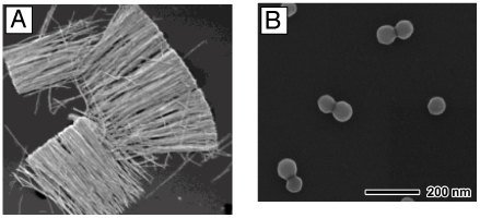 |
Little modification of nanostructures is needed; Large crystal assemblies are possible; Dimers and trimers can be formed. | Structures are often isotropic and difficult to control; Templates are often needed. |
| Polymer or SAM-mediated interactions | 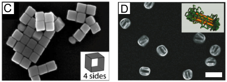 |
Interactions are anisotropic; Unique structures can be formed in solution | Nanostructures must be modified significantly for assembly. |
| Bond formation | 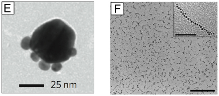 |
Particle spacing can be finely tuned; Bonds formed are automatically in areas of high enhancement; Structures can be formed in solution | Interactions are often isotropic resulting in symmetric structures. |
| Lithography | 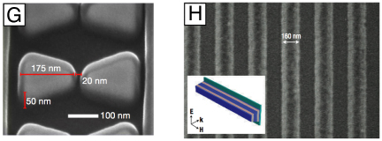 |
Complex structures and patterns are possible with known sizes, locations and orientations. | Limited resolution and scalability; Only possible with polycrystalline materials. |
5.2.1. Assembly with Electrostatic or Capillary Interactions
The simplest and most commonly used assembly techniques rely on isotropic interactions and are capable of creating both dimers and larger assemblies of nanoscale building blocks.355 In a typical approach, capillary and electrostatic forces are used to assemble nanostructures on a substrate.356 For example, the simple drying of an aqueous suspension of nanoparticles on a substrate generates a number of dimer structures through capillary forces. This technique has been used extensively in SERS studies as well as many other fundamental studies of LSP modes associated with dimers, trimers, and other aggregates.60,199 However, the yields of such aggregates are often very low and differentiating between different types of structures and determining their geometry with respect to the excitation polarization, while possible,213 is not simple or common with far-field spectroscopy techniques. A notable exception is Ag nanowires which can form oriented sheets or rafts via capillary and electrostatic interactions (Table 3A) which can be seen under an optical microscope.23,47,335,357
Recently, we have reported the synthesis of dimers consisting of single crystalline Ag spheres <30 nm in diameter with a yield >50% based on the polyol synthesis, in which growth and dimerization of Ag nanospheres were accomplished at the same time due to electrostatic interactions, as seen in Table 3B.358 Another similar method, based on wet etching with Fe(NO3)3, could also form well-defined dimers of Ag nanospheres with a range of different sizes.330 The etching reaction was performed at room temperature in ethanol with the help of PVP. When an aqueous suspension of Ag nanocubes was mixed with a small amount of aqueous Fe(NO3)3 solution in ethanol, the corners and edges of the cubes were truncated to generate spheres, which were also induced to dimerize at the same time. Individual dimers consisting of Ag spheres 40, 63, and 80 nm in diameter have been made in this way and their SERS properties were measured with the largest enhancement factor approaching 108.358
More complex methods have also been used to form 1D and 2D lattices of nanostructures via capillary and electrostatic forces.359 By manipulating the wetting and speed at which the substrate was withdrawn from a suspension of nanoparticles, capillary forces could assemble Ag nanoparticles into linear chains over large areas.350,361 Macroscopic 2D lattices of large Ag nanocubes, truncated nanocubes and octahedrons have also been formed using the Langmuir-Blodgett (LB) technique, followed by transfer to various substrates.346 A lattice of octahedrons fabricated using this method is shown in Figure 17C. While the particles assemble with simple isotropic interactions, their interparticle spacing and packing density can be controlled by particle concentration or presence of molecules on the particle surface. Films composed of truncated cubes and octahedrons display reflectance peaks at 480 nm and 710 nm, respectively, corresponding to the coupled quadrupolar modes of the ordered films. Despite their similar packing arrangement and interparticle spacing, each film exhibits a distinct optical response due to the shape dependence for the plasmonic properties of individual nanoparticles.346
Large 3D lattices assembled through isotropic interactions have typically used very small nanoparticles (1–5 nm) which are not well-suited for plasmonic applications.362,363 Recently, however, large Ag octahedrons (~150 nm in edge length) have been used to form large plasmonic lattices with a frequency-selective response in the visible wavelengths.364 These materials formed plasmonic bandgap structures which could be tuned by changing the periodicity of the nanocrystal and the crystal density. However, the nearest-neighbor LSP coupling within the lattice was found to be the dominant parameter in determining the optical response, which could be controlled by varying the extent of particle sedimentation.
The interparticle spacing can also be tuned by functionalizing the surfaces of the constituent nanostructures. For example, by using self-assembled monolayers (SAMs) of alkanethiolates with different chain lengths, it is possible to effectively manipulate the interparticle spacings.365,366 Molecules that react to heat have also been used to create dynamic gaps whose distance can change with temperature.367 Additionally, by performing isotropic assembly on an elastomeric substrate, it is possible to physically manipulate the interparticle spacing by stretching or compressing the substrate.368
5.2.2. Assembly with Molecular Interactions
Assemblies of nanostructures have also been formed in solutions with high yields by using molecularly mediated anisotropic interations.25,193,369 These techniques are possible due to more advanced synthetic methods for producing uniform Ag nanostructures with well-defined facets and better control over the binding of a variety of molecules to nanostructure surfaces. The binding of molecules to nanostructures will not always be uniform as the surface of an anisotropic nanostructure will typically be enclosed by different types of crystal facets, each with a different surface energy. These differences in surface energy can sometimes lead to preferential binding of specific molecules on one type of facet. For example, as discussed in the synthesis section, PVP preferentially binds to {100} facets and citrate preferentially binds to {111} facets of Ag.84
Thiols are an important class of molecules which can bind strongly to the surface of coinage metal nanostructures and form SAMs that cover their surfaces.370 These monolayers change the surface chemistry of the nanostructure, and can impart directionality to its interactions if the coating is not the same on all facets. The use of alkanethiolate SAMs to selectively assemble Ag nanostructures is shown in Table 3C. For Ag nanocubes, different cube faces could be selectively functionalized with either a hydrophobic or hydrophilic SAM by functionalizing a single layer of cubes dried on a substrate and then releasing them into solution with sonication.371 The cubes would then assemble in water via hydrophobic forces to minimize the number of hydrophobic faces in contact with the surrounding water. The resultant structures assembled so that their hydrophobic faces were in contact. Similarly, Au rods have been shown to preferentially bind polystyrene at their tips resulting in a hydrophilic rod with tethered hydrophobic chains at the ends.372 When water was added into the solution containing the rods, they began to assemble end-to-end to form chains due to polystyrene’s unfavorable interaction with the water. When the solvent was hydrophobic, clusters formed instead, as seen in Table 3D. Linear chains of Ag nanoparticles assembled using this technique reported SERS intensities that were several orders in magnitude greater than single nanoparticles.373
Other unique structures can be formed using reversible, anisotropic interactions which are more complex than the simple lattices formed through isotropic interactions.350,351 Using amphiphilic Ag nanoparticles, tube-like nanoarrays approximately 100 nm in length, 20 nm in diameter and with an interparticle gap of 3 nm, could be assembled in water. Bio-inspired templates, like viruses and micelles, can also provide scaffolds in solution that are well-suited for the reversible assembly of metal nanoparticles.351 In general, anisotropic assembly is ideal for creating nanostructures with unique suprastructures in solutions at high yields. In terms of plasmonic applications, these assemblies are often studied as proof-of-concept systems as they have unique and novel optical properties.322 However, more research is required for these structures to find practical applications.
5.2.3. Assembly Involving Bond Formation
When chemical bonds are used to form assemblies, the bonds that form between the constituent nanoparticles increase the stability of the structure (though increasing the temperature or introducing other molecules could potentially break them). This type of assembly often relies on the binding of complementary strands of DNA.348,352,374,375 DNA is a particularly useful molecule for assembly because of its availability and well-understood interactions. Also, as a biomolecule, it is compatible with sophisticated pre-existing biomolecules (e.g., proteins) that can change interparticle spacings or cleave the DNA linkage between structures using different enzymes.376 However, other methods, such as those that utilize photoswitchable molecules,354 and streptavidin-biotin377 can also be used to create bonds between nanoparticles. The benefit of this type of assembly is the high degree of control that can be achieved, and the complex assembly schemes that are possible due to the specificity of the molecules used to form bonds between nanostructures.
A number of structures have been formed from the hybridization of complementary strands of DNA- from dimers to 3D crystal lattices. For plasmonic applications, DNA is particularly useful because its length can be fine-tuned to create interparticle gaps that would not be possible using other techniques. This can be seen in Figure 17, where Ag dimers were formed with gap widths of 1 to 25 nm via DNA assembly.378 In Figure 17A and B, the SP energy (eV) was directly compared to the gap width and the laser polarization. As the interparticle gap was decreased, the gap SP red shifted (to lower energies) indicating a stronger coupling between the particles.
The “coded” nature of DNA can also generate interesting structures as seen Table 3E. This Janus cluster, a large spherical nanoparticle with smaller nanoparticles assembled on one side of the structure, was made using different DNA codes. The large particle was functionalized with the smaller nanoparticles on a substrate to protect one side of the large particle from functionalization.379 Such heterostructures are promising for near-field studies as their properties are different from the dimeric counterparts.193,380
One drawback with DNA-programmed assemblies is that the location of the DNA molecule on a nanoparticle’s surface cannot be easily controlled. In contrast, thiolate SAMs can sometimes spontaneously form non-uniform domains on the surface of a nanoparticle.381 When packing SAMS onto a spherical metal nanoparticle, unstable domains form at opposing ends of the nanoparticle’s surface due to unavoidable defect regions in the crystalline packing of molecules on a spherical substrate. These defect regions can be functionalized with reactive molecules capable of forming a covalent bond upon activation.353 Such functionalized nanoparticles can be assembled into linear chains, as shown in Table 3F. The self-organization of the thiolate ligands into patterns and stripes with a wide variety of spacings on metal nanoparticles has also been demonstrated and may be used in the future for anisotropic assembly of isotropic metal nanoparticles.350,382 Potential limitations of structures synthesized with bond formation is that the molecular linkers that bridge adjacent nanoparticles can prevent other molecules from entering the gap region (i.e., hot spot), or these linker molecules can interfere with signals needed for sensing and imaging applications.
5.3. Gaps Fabricated Using Lithographic Methods
Lithography is also an important tool for generating nanostructures with controllable gaps.382 These structures are typically well-defined and can be produced over large areas (cm2) and in multiple copies. Particularly, many fundamental studies have used the lithographically generated bow-tie structures for mapping and understanding near-field enhancement.332,333 In general, it would be very difficult or impossible to use other methods to fabricate the patterned arrays of metal strips, gratings, and holes essential to plasmonic waveguides and lenses.384,385 However, in comparison to assembly, lithography is not as good at producing gaps controlled below 10 nm. Lithography also can only produce planer, thin-film architectures. Three general types of gap structures are prevalent in lithography: i) periodic arrays of nanoparticles of the same shape and size; ii) nanoparticle clusters that create nanoscale gaps of different shapes and sizes; and finally iii) nanoscale gratings that provide long, one-dimensional gaps of varying depth and width. The methods discussed in Section 2.3 (EBL, FIB, and NSL) are often used to create these structures and many modified versions have been created to improve the controlled formation of gaps.
One of the challenges with using lithographic techniques to generate gap structures is the difficulty of patterning features only a few nm apart.165 For EBL and FIB, damage to the resist as well as ineffective lift-off at such small sizes can disrupt the uniformity of nanoparticle arrays and the shape of the particles, though direct EBL can eliminate many of these defects. For periodic arrays of nanoparticles generated using EBL, the gap size is limited to about 50 nm.386 FIB milling can also be used to generate gaps as narrow as 10–20 nm. This technique takes advantage of the destructive nature of bombarding a surface with ions, and can be used to carve out a nanostructured substrate with high resolution. First, a layer of Ag is deposited on a Si substrate, the thickness of which can be controlled by traditional PVD, typically 60–100 nm. Next, metal pillars are milled using a FIB according to a predetermined pattern. Examples of shapes that easily generate small gaps are square pillars in a checkerboard pattern, in which 20 nm gaps can be formed between diagonal corners of the pillars.387 More complicated structures, such as multi-pointed stars, are milled to maximize the number of gaps formed between the sharp points. The patterning of stars was shown to produce gaps as small as 10 nm.
In traditional NSL, the gap sizes are typically too large for plasmonic applications. However, modified versions of this method have been developed to solve these problems. For example, angle-resolved NSL (AR NSL) was developed to produce smaller gaps between nanoparticles by simply rotating the colloidal mask between Ag depositions.388 The first round of deposition is performed at an angle, which is measured as the angle between the deposition beam and the normal to the colloidal mask. To generate gaps, the substrate is then rotated in order to shift the projection of the gaps between spheres onto the substrate. A larger rotation will increase the size of the gap until the projection is blocked by the spheres themselves. Gaps as small as 4 nm have been fabricated this way.168
In addition to regular arrays of discrete particles, lithographic techniques can also be used to generate clusters of nanostructures and thin films of Ag with discrete holes. In these approaches, the geometry of the gap (or hole) is typically the focus, and the hole pattern will define the shape of Ag structures.185,389 One method that has been demonstrated for creating these structures is fabricating polymer pillars with EBL and then depositing Ag via PVD. This technique produced a variety of morphologies including star-shaped clusters of elongated nanopillars, which resulted in an array of pentagonal or hexagonal holes.386 As with arrays of nanoparticles generated by regular EBL, the interparticle gaps could be controlled as small as 50 nm, which depended on the resist and the thickness of the Ag layer.390
Nano-imprint lithography (NIL) has also been used to make nanoscale gaps, specifically, nanoscale grooves (1D gaps).391,392 However, the width of these gaps is still limited by the resolution of photolithography or EBL, as these techniques are used to generate the mold. Recently, novel variations on this technique have made it possible to generate grooves that are less than 10 nm wide.392 In the first step, deep UV (DUV) was used to generate arrays of Si nanowires. Since DUV uses wavelengths of about 190 nm, it can fabricate smaller features (~50 nm) on Si wafers than traditional photolithography. A layer of HfO2 was then deposited to reduce the spacing between the wires from 100 nm to about 50 nm or less. Finally, Ag film deposition yielded 10 nm gaps. Controlling the thickness of the Ag layer, as well as the size and spacing of the Si nanowires were two ways to tune the plasmonic properties of the substrate.33
Both solution-phase methods and lithographic techniques remain important to the assembly of nanostructures and the control over interparticle gaps. Future advances will likely take advantage of both types of methods depending on the desired application.3,4 One interesting aspect of the gaps between nanostructures that has not been thoroughly investigated is that even though gaps generated with lithographic and solution-phase methods can have the same shape, they may have different plasmonic properties due to the difference in crystallinity and surface roughness.393 A direct comparison between similar structures made by lithography and synthesis methods is needed to determine how the plasmonic properties of these materials are affected by their fabrication processes. Some of the factors that may cause differences are the limited coupling between thin-film nanostructures defined within the same plane and the effects of surface roughness and crystallinity.
5.4. Engineering Plasmonic Interactions between Nanoparticles and Substrates
Depositing nanoparticles onto substrates is often a necessity as this imparts a fixed location and orientation to the nanostructure with respect to its environment, which is needed to identify and study single nanoparticles effectively.199 A nanoparticle deposited on a substrate will have different properties compared with the same nanoparticle in a solution.191,190,207 The extreme sensitivity of plasmonic nanostructures to the refractive index of their environment is one reason why substrates can affect a nanoparticle’s optical properties. The other is that a nanoparticle on a substrate will experience an anisotropic environment. One side of the nanoparticle faces the substrate and one side does not. This can have unusual effects on the plasmonic properties of a nanoparticle that are not seen in isotropic environments.207 The substrate effect on a nanoparticle has only recently been investigated in terms LSPR peak shifting395 and splitting,208 and currently little is understood about how substrates effect the near-field properties (spatial distribution, strength, etc.) of a nanoparticle.47,200,337 A better understanding of particle-substrate interactions could have enormous benefits, as this configuration is ubiquitous in plasmonic research and easy to create. However, controlling the physical properties of a supporting substrate for plasmonic applications is still in its infancy.
When a nanoparticle approaches a dielectric substrate the environmental symmetry of the nanoparticle is broken and degenerate LSPR modes (i.e., different LSPR modes with the same energy) can be differentiated. LSPR modes that are in proximity to the substrate can interact with the substrate, and will have new properties. This interaction can have a significant effect on the nanoparticle’s scattering spectra which is typically observed as a red shift of the LSPR as a nanoparticle approaches a substrate.190 For a Ag nanocube approaching a glass substrate, as seen in Figure 8, the LSPR red shifts and splits into two peaks.200 From FDTD calculations, the peaks are assigned to LSPR modes with near-fields facing away (peak 1 at 430 nm) or towards (peak 2 at 550 nm) the glass substrate. Interestingly, the LSPR peak facing away from of the substrate (peak 1) was found to be much more sensitive to changes in the local environment compared to LSPR peaks of Ag nanocubes in a solution.
The reduced symmetry of a nanoparticle on a substrate can also cause the dipole LSPR mode of a nanoparticle to split into two modes: one oscillating parallel to the substrate and one oscillating perpendicular to the substrate.207 These LSPR modes can be separately excited by controlling the polarization of the incident light with respect to the supporting substrate.191,207 The permittivity of the substrate will also affect the formation and strength of LSPR modes. The higher the permittivity, the greater the interaction between the nanostructure and the substrate, and larger shifts in the LSPR are often observed.207 The distance between the nanoparticle and substrate will also determine the strength of their interactions.
In contrast to dielectric substrates, the interactions between a metal substrate and a metal nanoparticle are more complicated and potentially much more interesting. Metal substrates (like evaporated thin films, 10–200 nm in thickness) can support PSPs which can interact with metal nanoparticles creating a strongly coupled plasmonic system.396 The hybridization between a metal nanoparticle and metal substrate can fundamentally change the LSP modes supported by the nanoparticle. This can have profound effects on the near-fields of the nanoparticle, which may prove beneficial to surface-enhanced spectroscopies like SERS and SEF. In Figure 18, SERS enhancements from a single nanowires were found to be 10× larger when the nanostructure was on a metal film compared to a Si substrate.47 In fact without the use of a metal film no SERS spectra could be detected from the molecule benzenethiol (BT) as shown in Figure 18B. When either Ag or Au films were used, the SERS enhancement was more sensitive to the composition of the nanowire. Single Ag nanowires had larger SERS enhancements compared with Au nanowires on a metal substrate by a factor of 2×. Metal substrate effects are also sensitive to the distance between the nanoparticle and the substrate,395 but relatively little is known about the effects of metal substrates on the plasmonic properties of nanoparticles. While several theoretical studies focus on the plasmonic interactions between a metal nanoparticle and substrate,190,397 additional studies are required to determine if metal substrates can be used to effectively control the plasmonic properties of supported nanoparticles.
Figure 18.

(A) The FDTD calculated E-field enhancements (|E|2) of a Au nanowire on a Au film and Si substrate, respectively. The near field intensities are larger for the nanowires on the metallic film. (B) SERS measurements of the molecule benzenethiol (BT) from a single Au nanowire on a Au film (blue line) and on a Si substrate (green line). Reproduced with permission from [47]. Copyright 2008 ACS.
6. Plasmonic Applications of Silver Nanostructures
Plasmonics encompasses a fundamental light-matter interaction, consequently there are many scientific fields that stand to benefit from it. Already, many applications of plasmonics have emerged in past decades like SERS, near-field optical microscopy, and LSPR-based sensing. Despite this wide range of research activities, current applications of plasmonic nanostructures can generally be categorized into three thrusts: i) LSPR sensing and detection, ii) concentration of light to enhance or manipulate the optical response of nearby molecules, and iii) manipulation of light with plasmonic circuitry. The first thrust area takes advantage of the sensitivity of a nanostructure’s LSPR properties toward its surroundings. The second exploits the intense E-fields and highly directional nature of LSPRs supported by nanostructures (in this context they are often called nano-antennas) to enhance molecular scattering or emission cross sections and, in some cases, control the directionality of light propagation. Finally, the third encompasses the guiding and manipulation of PSP modes in one-dimensional nanostructures. Below we discuss some recent applications in the thrusts noted above, as well as emerging applications and future directions of plasmonics.
6.1. Surface Plasmon Resonance Sensing and Detection
Some of the first, and most successful, applications of plasmonic structures were in the detection of molecules. This technique has been commercialized for PSPs on continuous metal films.398 The films are chemically functionalized to selectively bind target molecules like DNA strands or proteins. Upon binding of the target molecule, the dielectric environment near the surface of the metal film is altered. Consequently, binding can be monitored by measuring the change in coupling geometry (i.e., the angle) between the metal film and the excitation source required to generate PSPs.5,27 This technique remains important and a number of commercially available instruments are widely used today in the biological sciences.
This technique has been extended to LSPR sensing with nanoparticles. Analogous to the change in coupling geometry for the metal film, when the dielectric environment around a plasmonic nanoparticle changes due to the introduction of analyte molecules, the resonance frequency of the LSPR will shift.35,394,399,400 This is the foundation of LSPR sensing, and by carefully preparing the nanostructures to interact only with specific molecules, molecular binding affinities, reaction rates, conformational changes, and complex interactions can all be monitored with this technique. There are several excellent reviews of this type of chemical sensing for further reading.19,20,401,402
While the examples so far all involve LSPR-based sensing of molecules, other changes can also be detected via LSPR techniques. Recently, the structural changes of a nanoparticle, typically associated with aging and minimization of its surface energy,131 have been used to develop a novel class of colorimetric indicators for time and the average temperature over extended timeframes.246 For example, the sharp corners of triangular Ag nanoplates in solution will round and become truncated over time resulting in a large shift in the LSPR. This rounding process was found to be sensitive to temperature. At higher temperatures the rounding process proceeded faster. These variables (time and temperature) could be calibrated to the LSPR shift of the Ag nanoplates. The color change that accompanies this rounding can be seen with the naked eye, making this new system well-suited as time and temperature indicators. When placed on the outside of a product’s packing, the time and temperature information of the product can be easily determined.
More recent advances in LSPR sensing and detection have focused on increasing the LSPR sensitivity of metal nanostructures. For example, coupling a resonant molecule to the resonance frequency of a nanostructure can increase the magnitude of the nanostructure’s LSPR peak shift dramatically.403–406 Strong resonance coupling between a molecule and a nanostructure can occur when there is a spectral overlap between the LSPR and a molecular electronic resonance.407 This coupling is sensitive to the electronic structure of the adsorbate and can create a large spectral shift compared to non-resonant molecules. This new technique allows for LSPR detection of a small number of molecules that would not be able to significantly change the surrounding refractive index of the metal nanostructure for appreciable LSPR shifts. Instead these molecules can interact with the bound resonant molecules on the nanostructure and change their electronic structure. In one study, the electronic structure of the heme-containing cytochrome P450 protein (adsorbed on Ag nanostructures) was altered by the binding of camphor. LSPR shifts as large as 67 nm were observed, corresponding to a shift of 0.07 nm per camphor molecule.404 This technique has the potential to make LSPR sensing sensitive enough for single-molecule detection. However, the fundamental interaction between the resonant molecule and the nanostructure requires further study before this technique is fully optimized.
Another method to increase the sensitivity of LSPR sensing takes advantage of the distance dependent coupling between nanoparticles.378,408–410 As described in Section 5, the SP hybridization of nearby nanostructures can result in a fundamentally new SP mode which is typically red shifted (up to 70 nm) relative to those of the constituent structures and the shift is very sensitive to the gap width between the structures (~10 nm for every 1 nm in distance). By modifying nanoparticles with proteins and ligands that will induce aggregation when they bind, molecular interactions can be inferred from these gap-dependent LSPR shifts. The number of molecules trapped in the gap region is typically very small and the resulting spectral shifts are very significant. The shifts can be seen with the naked eye for suspensions of nanoparticles, or with a microscope for single dimers.
LSPR sensing using distance dependent coupling was first accomplished by forming large aggregates via DNA.411–413 These experiments were first monitored by observing the color change of the solution (colorimetric detection), and this continues to be an effective way to monitor a number of different processes like enzymatic activity414 and to detect heavy metal ions such as Hg.415 These techniques measure the interactions of many millions of nanoparticles. In contrast, more recent studies have focused on single dimers or “plasmon rulers” by calibrating LSPR shifts to the width of the gap within a dimer,231 monitoring the changes in scattering intensity due to dimerization (there can be a 5× increase), and the optical polarization dependence for the dimer structure.376,416,417 The most innovative studies have used the gap width dependence to monitor dynamic changes in the separation between nanoparticles (typically a dimer structure) and the associated molecules.376,418 These plasmon rulers can be monitored over long periods of time and gap distances from a few nanometers up to 70 nm can be determined. Both capabilities represent significant improvements over systems based on molecular dyes.419 In addition, DNA bending376 and cleavage376,417 can both be monitored this way, as well as any enzyme that can modify the length of DNA.
These plasmon rulers have also been used in vitro to probe cellular mechanisms.418,420,421 In Figure 19, Ag dimers connected by DNA were used to probe the compartmentalization dynamics of a cellular membrane in a novel technique called polarization-resolved plasmon coupling microscopy.418 The rotational and translational motion, as well as gap width (g) within a dimer were monitored in real-time for many individual dimers deposited on a cell surface (see Figure 19B). As confinement increased, the particle separation decreased and there was less mobility. Figure 19C shows a spatial map of g values where the shortest interparticle spacing was confined to three well-defined regions (C-1, C-2, and C-3). A reduced rotational movement (determined from polarization measurements) was also correlated with these regions. These observations show that confinement to an area on a cell membrane does affect rotational motion and the average interparticle spacing of the plasmon rulers. These areas were consistent with length scales of cell compartmentalization, confirming that organizational heterogeneity in a cell membrane occurs at scales well below the diffraction limit. The “dance” of plasmon rulers confined to the cell membrane is an ideal technique for studying the ebb and flow of the cellular surface at resolutions much higher than can be achieved with traditional particle tracking.418
Figure 19.

(A) Dimers of Ag nanoparticle plasmonic rulers and can serve as probes in polarized resolved plasmon coupled spectroscopy which probes the dynamics of cell surfaces. (B) The dark field scattering image of plasmonic rulers on a HeLa cell at two different scattering polarizations are shown. The red box corresponds to scattering from one dimer which is tracked over time on the cell surface. (C) Spatial analysis of interparticle gap width (g) of plasmonic rulers on a cell. Confinement on the cell surface is expected to decrease g. The map shows three regions (C1–C3) on the cell membrane were the plasmonic rulers were confined and these regions also have smaller interparticle spacings. Reproduced with permission from [418]. Copyright 2010 ACS.
6.2. Focusing and Concentrating Light with Nanostructures
In contrast to LSPR sensing, the enhanced E-fields near a nanostructure’s surface provides a relatively simple route to single-molecule detection,250,338,422 and control over the optical properties of molecules. In general, the strongly confined fields near a metal nanostructure can tremendously alter the light-emission, excitation, and collection efficiency of nearby molecules and optical emitters like quantum dots (QD).6 The measurable parameters include both the intensity of the emitted light,250,339,344,423,424 its directionality,344,425,426 and even its polarization.329,347 Nanostructures that are engineered to focus and manipulate light are often called nano-antennas and are typically nanostructures with sharp features or dimer structures with engineered sizes and gap widths.
6.2.1. Surface-Enhanced Raman Scattering
In SERS, the enhanced E-fields of a plasmonic nanostructure can increase the Raman scattering of molecules in their vicinity by a factor of E4.248,340,427 Measured enhancements range from 104 to 1015 and even single molecules have been detected with dimers of nanoparticles and larger aggregates.60,338,422,428,429 SERS provides the unique vibrational spectrum of a molecule, a Raman fingerprint, and does not require labels or other markers (although these are often used). It also does not just infer the presence of a molecule through spectral shifts, but can directly identify its structure based on the spectroscopic fingerprint. For these reasons SERS is a direct and sensitive technique, and its use has been actively explored over the past decades.342,430,431
The enormous enhancement in SERS can be attributed to two mechanisms. The first is a result of electromagnetic enhancement that arise due to the LSPR modes which can focus light into nanosized volumes, drastically increasing the E-field intensity near the nanoparticle.35,36,234,235 The second is chemical enhancement, which is thought to arise from interactions between the molecule and the nanoparticle as a result of changes to the molecular electronic states. This leads to resonant enhancement from molecular excitations or charge transfers between the molecule and the nanoparticle.432,433 The electromagnetic mechanism is typically thought to contribute most of the enhancement (105–108) and the chemical enhancement contributes much less (10–103), however this remains an active area of research.332,434 The larger contribution of the electromagnetic mechanism has made this a favorite handle for engineering SERS, and many synthetic methods now exist to create plasmonic nanostructures than focus light into tiny volumes for electromagnetic enhancements. Dimers of nanoparticles and sharp features on nanostructures are excellent examples of attempts to focus light for SERS applications.
Due to the sensitivity of SERS and the extreme localization of enhanced E-fields, much of the work with SERS is an attempt to create nanostructures with reproducible and controllable enhancements.199,342 Correlating the physical structure (size, shape, morphology, and composition) with SERS enhancements has advanced both the understanding of SERS and the techniques used to control the assembly of nanostructures.47,335,345,435–437 Characterization of single particles or dimers has shown that shape, size, composition (Ag vs. Au), and excitation polarization all affect SERS enhancements.47,48,438–442 More recent studies have attempted to probe the hot spot (the region with the highest E-field enhancement) in single particles and dimers in an attempt to detect single molecules or determine the relative contribution of the hot spot to the SERS enhancement factor.60,202,331,335,338,358,422,443
From an application standpoint, SERS typically uses two strategies. In the first strategy, people attempt to capture and identify molecules in the local environment for ultrasensitive detection.430,444–446 The second strategy relies on the use of pre-determined molecules to create SERS “tags” or Raman molecules with unique and strong SERS signals.447–450 These molecules have unique SERS spectra, and, due to the narrow widths of Raman bands, are ideal for identifying and imaging numerous different tags in the same spectrum, a technique commonly known as multiplexing.448–450 An example of this technique is shown in Figure 20, A and B, where SERS tags are used for in vivo cancer imaging.451 Silver nanoparticles are functionalized with dye molecules that serve as the SERS tags and antibodies that preferentially bind to the receptors on tumor cells. Using excitation in the NIR, penetration depths up to a few centimeters were possible and small (~0.03 cm2) tumors could be identified and located non-invasively using a Raman system.
Figure 20.

(A) A photograph of a mouse with a tumor that has been labeled with SERS tags for non-invasive tumor detection with SERS. A laser is focused onto the tumor site and the SERS signal from the tumor is recorded. (B) The SERS signal from the tumor and liver of the mouse. The SERS signal from the tumor is representative of the SERS tag used to target the tumor, in contrast there is little signal from the liver. Reproduced with permission from [451]. Copyright 2008 Nature. In (C) nanoparticles functionalized with pH sensitive molecules are introduced into cells. The pH can be determined by monitoring the SERS bands (at 1423 cm−1 and 1076 cm−1) from the nanostructures and subendosomal resolution of the pH inside a cell can be achieved in real time. Reproduced with permission from [452]. Copyright 2010 ACS.
In Figure 20C, the rich spectral information, high spatial resolution, and sensitivity to changes in the probe molecules of SERS have been combined to map the pH inside living cells at subendosomal resolution.452 Silver nanoparticles with special SERS probe molecules attached were taken up by living cells. The cells were then scanned with a Raman microscope and two bands in the SERS spectra were used to determine the pH across different regions in the cell over time. The SERS probe molecules were nonresonant with the excitation so there was no photodecomposition for the probe molecule, and a broad range of excitation wavelengths could be used. Because the pH was derived from two Raman lines, no subtraction of background signals was required. This technique, therefore, offers significant advantages over fluorescence-based methods. The SERS pH measurements were consistent with the current understanding of the endocytotic pathway of metal nanoparticles and present a novel way to probe intercellular processes.452
6.2.2. Surface-Enhanced Fluorescence
The emission of resonant molecules in the vicinity of a plasmonic nanostructure can also be enhanced through a process known as surface-enhanced fluorescence (SEF).336,453,454 SEF occurs primarily as a result of the interactions between the excited state of a fluorophore with the near-fields of an excited metal nanostructure, increasing the optical excitation rate and the decay rate (both radiative and non-radiative) for the molecule. Plasmonic nanostructures can increase the emission intensity by pE2.454 Enhancement factors vary from 2–1,000 and are extremely sensitive to experimental parameters, making comparisons between different experiments difficult.250,336,455
Metal nanostructures can also alter both the radiative and non-radiative decay rates of nearby fluorophores, thereby changing their fluorescence lifetimes and quantum yields.250,341,344,456–458 Figure 21A shows a comparison of the lifetime images of two fluorescently stained cells grown on either a glass cover slip or a Ag nanoparticle island film (i.e., Ag nanoparticles deposited on a glass cover slip).459 The fluorescence from the stained membranes of the cells on the Ag film had a lifetime that was 2.0 ns shorter and had a 3× larger photostability due to SEF. This shorter lifetime allowed for more emission cycles prior to photobleaching, and the cell images are consequently brighter and more detailed. In a related study, the cell nucleus was stained (instead of the cell membranes) and deposited on a Ag island film. In this case the fluorescence images did not show any significant lifetime reduction or emission enhancement. This was attributed to the larger distance between the cell nucleus and the underlying Ag substrate as compared to the cell membrane, which was adjacent to the substrate. SEF could have a large impact on fluorescence imaging, but many variables like the distance between the flourophore and the nanostructure and its effect on excitation rate and fluorescence require further study.339,460–462
Figure 21.

Controlling radiative emission with plasmonic nanostructures. (A) Cells were seeded on glass coverslips (top) and on Ag nanoparticle island films (bottom), and fluorescence lifetime images were taken. The longer lifetime corresponded to enhanced fluorescence emission and was a result of the plasmonic Ag films. Reproduced with permission from [459]. Copyright 2008 ACS. (B) Nanoparticle aggregates (top dimer, bottom trimer) and corresponding plots of depolarization ratios with 583 (red line) and 555 (black line) nm excitation. For the dimer, the polarization of emitted light is along the interparticle axis, as expected. Breaking the symmetry of the dimer and forming a trimer results in polarization that is wavelength dependent and is rotated due to the third particle. Reproduced with permission from [329]. Copyright 2008 PNAS. (C) A quantum dot (QD) is placed near a Ag nanowire to generate a guided single PSP (shown in red) along the nanowire, where Γrad and Γpl are the emission rates into free space or guided plasmon modes, respectively. (D) A fluorescence microscope image showing the excited QD (red circle) and Ag nanowire (not visible) whose ends radiated excited plasmons (blue circle). Reproduced with permission from [489]. Copyright 2007 Nature.
Just like in SERS, the distance of the molecules from the plasmonic nanostructures can also affect the SEF experiments drastically due to the rapid decay of near-fields on the nanostructure and interactions between the molecule and metal nanoparticle itself.463,464 Current studies suggest that the fluorophore must be within ~30 nm of the metal nanostructure to benefit from the enhanced near-fields of the nanostructure.423 However, when a fluorophore is located too close (e.g. a few nanometers) to the metal nanoparticle, non-radiative relaxation rates can dominate and quenching arises, which can eliminate the benefits of LSPR excitation.460–462,465 While SERS and SEF have many similarities, they are very different,466 and, unlike SERS, fundamental studies of SEF have only begun to unfold in probing this interesting and useful phenomenon.461
6.2.3. Control of Light with Plasmonic Antennas
Antennas, like radio antennas, can collect and transmit electromagnetic waves. Similarly plasmonic antennas can collect electromagnetic waves and transmit them, but at optical frequencies. Also similar to radio antennas, the directionality of the transmitted electromagnetic wave near a plasmonic nanostructures can be controlled.425,426,467 Unlike typical antennas though, plasmonic antennas can also control the emission of nearby molecules. For example, the angular emission of a single molecule coupled to a single plasmonic antenna will be determined by the direction of the main SP mode of the antenna regardless of the molecule’s orientation.468 As such, a one-dimensional array of metal nanoparticle antennas can modify the spatial radiation pattern and the direct emissions to a single direction.469,470
More complex arrangements of plasmonic nanostructures can also control the polarization of the emitted light, as seen in Figure 21B.329 For dimers of Ag nanoparticles, the depolarization ratio (the intensity ratio between the perpendicular and parallel component of the scattered light), ρ(θ), is typically wavelength independent.471 Figure 21B (top-right graph) shows that the highest intensity of scattered light from a nanoparticle dimer occurs along the interparticle axis, which is expected. The addition of a third particle, as shown in the bottom image of Figure 21B, breaks the symmetry associated with the gap SP mode of the dimer. Consequently, the trimer exhibits wavelength dependent rotation of the polarization. The depolarization ratio for two excitation wavelengths are shown in Figure 21B, (bottom-right graph), with 555 nm in black squares and 583 nm in red circles, and they are shifted from one another. In the trimer system, polarization of the scattered light was also affected by the size, shape, and composition of the additional nanoparticle, as well as its distance from the dimer.329 When a small nanoparticle was added to a dimer made of larger nanoparticles, its effect on changing the polarization of the scattered light was minimal. For a more pronounced effect on the polarization, the third particle needed to be larger than the nanoparticles in the dimer and close (~1 nm) to them. Trimers (and higher order structures) clearly have unique properties ideal for light modulation and control, and more complex structures continue to be developed.322,373
Plasmonic nanostructures can also control emission from hybrid structures consisting of both semiconductor emitters and metal nanostructures.472–477 These hybrid structures are characterized by plasmon-exciton interactions and typically involve a QD and a plasmonic nanostructure. Enhancement of QD emission can result from the intense E-field enhancement near the nanostructure, and quenching can result from energy transfer from the QD to the metal nanostructure.478 Both are beneficial: increasing the emission and reducing decay lifetimes of QDs are both important to improve QD efficiencies for applications in sensing,477,479,480 solid state-lighting,481 and imaging.482,483 Energy transfer from a QD to a plasmonic structure can also result in highly coherent PSP modes (with single frequencies) which have potential applications in lasers,484,485 plasmonic transistors,486 and quantum computing.10,487,488 In Figure 21C, a CdSe QD couples with an Ag nanowire to generate single PSP mode at an optical frequency. The plasmon-exciton conversion was nearly 50% and a single PSP mode was generated from an optically excited QD which was then emitted at the distal end of the nanowire (Figure 21D).489 The size, shape, and arrangement of metal and semiconductor nanostructures can all affect plasmon-exciton interactions.478,490,491 For example, the nanowire radius will affect the coupling efficiency between the emission of QD and the PSP modes of the nanowire.478 These interactions have also been used to detect DNA and proteins based on fluorescence quenching, primarily by changing the distance between the exciton and plasmon.477–480
6.3. Plasmonic Circuitry
Integrating optical and electronic circuits could make it possible to greatly increase the speed and reduce the size of microprocessors.13,492 Currently, integration of optical interconnects into electronic circuits is not feasible due to the large size of optical components (1000× larger than electronic components). However, plasmonic nanostructures can carry optical signals at sizes comparable to those of the state-of-the-art transistors (<50 nm). Plasmonic circuits can also route electric currents, which may be useful in some applications.
Metal nanostructures that support PSPs are ideal for plasmonic circuitry. Unlike metal thin films, nanostructures inherently guide at scales below optical wavelengths,493 and are well-suited for integration (i.e., coupling) with other components. The main challenges in the use of chemically synthesized nanostructures are the difficulty in controlling their locations on a chip with accuracy at the nanometer scale, and dissipative losses of the PSPs (a problem with all plasmonic waveguides).4,494 Therefore, lithographic techniques are commonly used to generate plasmonic circuitry,22,458,489,495 which can eliminate the difficulties associated with nanowires in terms of control over their location, orientation, and geometry with respect to the environment. However, nanowires and other structures made from solution-phase synthesis techniques, have unique features (e.g., high crystallinity and smooth surface) not found in lithographic structures and will continue to play an important role in PSP waveguiding, as is evident by their presence in the most recent breakthroughs in plasmonic circuitry.17,22,23,182,357,458,489,495,496
Several types of nanostructures have been used as waveguides, including nanowires23,33,244 and “chains”’ of metal nanoparticles.497,498 Figure 22A shows a near-field scanning optical microscopy image of PSP modes supported by a Ag nanowire. The wire was excited on one end (not shown) and PSP modes were emitted at the opposite end of the nanowire. The modulation of the PSP can be seen in the image and the main PSP wavelength was 414 nm under 785 nm excitation.244 Many experiments have used Ag nanowires as waveguides, and found resistive heating within nanowires can limit the PSP propagation length. For example, recent studies with Ag nanowires (25 nm in diameter and 50 µm long) showed that the maximum length of propagation, as visualized by fluorescent markers, was ~15 µm.257 Solutions to attenuate energetic losses are needed for propagation distances on the millimeter scale. Chains of Ag nanoparticles represent one proposed solution, as there have a reduced metal volume and the resonant structure of the nanoparticles can be used to guide the light.498–500
Figure 22.

Plasmonic waveguides based on Ag nanowires. (A) A nearfield image of a propagating surface plasmon along a Ag nanowire. At the end of the nanowire the plasmon radiates into space. The inset shows a 2 µm section of the scattering intensity. Reproduced with permission from [244]. Copyright 2005 APS. (B) Branched Ag nanowires can be used to route plasmons. By controlling the polarization of light (red arrow), the plasmons can be routed to different nanowire branches as seen in the optical image (top). The same structure is shown in the bottom SEM image, with the inset showing the nanobranch junction. Reproduced with permission from [357]. Copyright 2010 ACS. In (C) a polymer waveguide (white line running diagonally across the image) and Ag nanowires are illuminated with white light (left image). In the right image the same area is shown, but with the waveguide illuminating the nanowires. The three labeled nanowires clearly show nanoscale guiding of light from the center of the waveguide to outside it. Reproduced with permission from [17]. Copyright 2008 Nature. (D) The plasmons from a Ag nanowire detected using a field-effect transistor. In the reflection image (with color overlay indicating electrical current (I)) the violet circle (I1), indicates the detected signal corresponding to the QD emission into the nanowire. The blue circles correspond to detection of PSPs launched by excitation from the laser at the ends of nanowire. The green circle corresponds to a QD away from the Ag nanowire. In the adjacent graph the current from the excitation of the QD (I1) and the nanowire (I2) is measured as a function of wavelength. The peak at 655 nm in I1 (violet line in graph) represents the electrical detection of the emission from the QD. Reproduced with permission from [181]. Copyright 2009 Nature.
Routing and manipulating the propagation direction of PSPs is also important for realization of integrated plasmonic circuits. There is a basic need for information carried by a plasmonic structure to be moved to different locations of a circuit.501,502 Fortunately, PSP propagation is not limited to straight lines and PSP modes within a nanowire can be bent and split.23 In Figure 22B, the PSP propagating down a “branched” Ag nanowire coupled to, and continued to propagate along, the branch as well as the main wire. Not only can these structures effectively split the PSP, but the PSP can be directed to either the main or branch wire by controlling the excitation polarization and/or wavelength.357 The routing was efficient and switching ratios (how well the PSP can be routed to different coupled nanowires) between the main and branched wire were close to 8. The switching and routing behaviors of the branched Ag nanowires can work simultaneously and independently for multiple wavelengths, providing a flexible handle for controlling PSP propagation.
The efficient coupling of input radiation into a nanoscale waveguide is also challenging due to mode mismatch and (for nanowires) polarization requirements. Typically a laser beam is focused with a dielectric lens onto one end of a nanowire, and if the laser is polarized along the wire’s long axis then the laser will excite the PSP modes of the nanowire. Focusing light in the center of the nanowire, or at the ends with polarization perpendicular to the wire’s long axis, does not result in coupling.23 A better approach is shown in Figure 22C, where a polymer waveguide (orientated perpendicular to the nanowire’s long axis) can excite PSP modes of several Ag nanowires at once.17 The optical waveguide effectively coupled to the Ag nanowires and directed the PSP far beyond the region of the nanowires embedded in the polymer. The coupling could also be controlled by the excitation polarization (coupling occurred when light was polarized parallel to the nanowires) and coupling to multiple nanowires could be achieved as long as they had one end close to the polymer waveguide.
A simple plasmonic circuit is shown in Figure 22D, illustrating efficient exciton-plasmon-electronic coupling using both a Ag nanowire and a QD.182 The plasmons were detected by a Ge nanowire field-effect transistor and detected as current (I) with ~0.1 electrons per plasmon. The electrical detection of plasmons is an important step in the creation of plasmonic circuits without optical components (lenses for example), and may allow for detection of SP modes that cannot be detected optically due to suppression by symmetry.192 With advancements in electrically driven SP sources,503 plasmonic circuits could also be engineered without the need of far-field radiation or detection techniques. In Figure 22D (right panel), the ability of the QD to couple with the nanowire was measured as current (I1), which had a peak at 655 nm, indicative of a highly coherent PSP mode. Single-plasmon emitters are important components of plasmonic circuits and many applications (like single-photon transistors11) stand to be realized with better understanding of their properties.504
6.4. Emerging Applications
While the ability of plasmonic nanostructures to concentrate and direct light has already made them powerful materials for the applications discussed above, new applications are emerging in a broad range of areas, which are a testament to the recent advancements in the synthesis and assembly of Ag nanostructures.16,49,77,236,505 Some of the most exciting examples are in areas, or devices, such as photovoltaics,14,506,507 active plasmonics,405,508 superlenses,509–511 and lasers.484,485,512,513
One of the primary challenges in photovoltaic cells is to efficiently harvest light energy across the solar spectrum. For this reason, implementing light harvesting nanostructures at specific locations to trap more light and/or localize it for the optimal generation of electrical energy are interesting and important areas of research.14,514–516 Both LSPs and PSPs can be employed for these purposes. In one approach, metal nanoparticles were used as subwavelength antennas, where the near-fields of the nanoparticles were coupled to the semiconductor layer, generating electron-hole pairs and increasing the absorption cross section (Figure 23A).14 Studies using Ag nanoparticles embedded in organic solar cells were found to have enhanced efficiencies using this technique.506 In QD-based solar cells, where the bandgap can be easily tuned by changing the QD’s size, thick QD layers are necessary for effective light absorption, making carrier transport problematic. When light harvested from plasmonic nanostructures is coupled to the QDs, it is possible to reduce the thickness of the cell and thus enhance the efficiency.517
Figure 23.

Emerging applications of plasmonic nanostructures. (A) Metal nanoparticles (dark circles) embedded in a solar cell effectively trap light in the semiconductor, increasing the cross section and creating electron hole pairs near the P-N junction. Reproduced with permission from [14]. Copyright 2010 Nature. (B) A nanostructured laser based on plasmonics, surface plasmon amplification by stimulated emission of radiation (SPASER), emits coherent light at 531 nm (red line, labeled 4) with excitation at 488 nm (blue line, 2). The spaser generates stimulated emission of surface plasmons in resonating metal nanostructures adjacent to a gain medium. The normal extinction spectrum (green line, 1) and the spontaneous emission (black line, 3) are much broader compared to stimulated spectra. Reproduced with permission from [484]. Copyright 2009 Nature. (C) In active plasmonics, resonant molecules can couple with the LSPR of nanostructures allowing for active control over resonance conditions that change the optical properties of the nanostructure. Reproduced with permission from [406] Copyright 2010 ACS. (D) Metal nanorods are organized to create a proposed superlens which can transfer color images of nanometer-sized objects to the far field for observation. Reproduced with permission from [510]. Copyright 2008 Nature.
Another potential application of plasmonics deals with the creation of tiny lasers based on metal nanoparticles and a gain medium.513 In conventional lasers, a photon interacts with an electron, resulting in its transition to a lower energy level, and creating another photon that is identical to the original. If these photons are reflected repeatedly in the gain medium then a cascading effect is produced. This is known as stimulated emission and is the principle on which lasers function.518 The nanoplasmonic equivalent to conventional lasers is the surface plasmon amplification by stimulated emmisson of radition (SPASER). In a SPASER, the LSPR modes provide the feedback needed for stimulated emission of dye molecules in the presence of metal nanoparticles. SPASER represents a new way of controlling plasmon emission from nanostructures.512,513,519–521 These structures can actively generate coherent LSPRs when excited through a gain medium. Figure 23B shows a recent example based on a Au nanoparticle inside a dye-doped silica shell. Pumping at 488 nm resulted in stimulated emission from the nanoparticle at 530 nm. While a gold nanoparticle was used in this example, simulations suggest that Ag may be a better candidate as less gain may be needed to overcome the loss intrinsic to metal nanostructures.512 A SPASER can excite a single LSPR mode in a nanoparticle, something nearly impossible with external optical fields, and their LSPR emission could be tuned to nearly any wavelength (below optical wavelengths), ideal for photolithography below the diffraction limit. Furthermore, dark modes (SP modes that cannot be excited by optical means) can be excited in SPASER, producing a non-radiative, background-free light source and opening up a new arena of SP modes for manipulation and study.59
A third emerging area of plasmonics is active plasmonics where plasmons can be “turned on” or modified by molecules,405,406 phase changing materials,522 and polymers.523 The ability to actively control plasmons is needed for plasmonic modulators512, 519 and switches,503 which would be integral components of any plasmonic circuit. For sensing applications, the ability to enhance plasmons or selectively turn them on can also aid in selective detection. In one recent example, a supramolecular chromophore generated via the complexation of two molecules (known as host-guest binding) was coupled with the LSPR of a metal nanostructure. The host molecule was immobilized on the surface of the metal nanostructure and when the guest molecule binded, together they created a chromophore engineered to be in resonance with the LSPR of the nanostructure and the excitation wavelength. The strong interaction between the nanostructure and the supramolecular chromophore changed the LSPR properties dramatically, increasing the absorbance intensity and generating resonant conditions ideal for SERS (Figure 23C).406 Upon removal of the guest molecules, the nanostructure retained its previous properties. Similarly, molecular motors can also be used to actively change and control LSPRs by changing their electronic transitions to match LSPR frequencies.405 Using molecules, polymers, and other related materials to control plasmons will likely become an integral part of the toolbox for engineering plasmonic responses.
Plasmonic nanostructures have also been used to fabricate superlenses which can create images of structures below optical wavelengths (~60 nm).2,9,509 The ability to “see” DNA and other objects well below the wavelength of visible light is a tantalizing prospect that grows closer to reality. In a superlens, evanescent waves are enhanced with surface plasmons, and gain magnification to produce images of subwavelength features.8,525 Silver films were used as the first example of superlenses, which exhibited resolutions 5× better than typical optical lenses.8, 509,526,527 Problems with previously reported superlenses include their ability to operate only at a single frequency, high losses (in terms of SP energy), and finally that the image is not detectable in the far-field. The last problem requires that a photoresist must be used to develop the image which is then visualized with techniques like atomic force microscopy. New designs of superlenses, however, may soon solve these problems. For example, Ag nanowire and nanobar arrays may be able to image in color and in the far-field.510,528 Figure 23D shows such a structure with nanorods as a key feature. Short nanorods, as opposed to Ag films, for example, are needed as they support strong LSPR modes at optical frequencies and thereby allow for color imaging. Furthermore, by tapering the stacked layers of rods outward from the object plane the image plane can have a large pixel-to-pixel distance, and can potentially be seen with the naked eye.510 These new designs, when implemented, would be a significant improvement over past superlenses and may allow for imaging below optical wavelengths in configurations consistent with current microscopy.
7. Concluding Remarks
The extensive research into plasmonic nanostructures in recent years has proven them to be a powerful platform for the manipulation of light. Due to its strong optical response and low cost, Ag has been the metal of choice for much of this work. Many of the advances in this field have been made possible due to progress in both the synthesis and assembly of Ag nanostructures. Through solution-phase methods, lithographic techniques, and combinations of the two, a large number of nanostructures (both simple and complex) can be produced. This long list includes large-scale syntheses of fundamental geometries (such as spheres, cubes, octahedrons, and triangular plates) with precisely controlled sizes and high uniformity, nanostructures with sharp features to create regions of high field enhancement, and hybrid structures containing more than one material. Importantly, detailed investigations into the growth mechanisms in these syntheses have illuminated a number of critical factors that determine the final geometry, such as twinning, oxidative etching, and surface capping. These insights should enable even greater control over Ag nanostructures in terms of size and morphology in the future.
One of the reasons that so much attention has been focused on the synthesis of novel Ag nanostructures is that physical features such as size and shape are some of the most powerful handles for controlling and manipulating the plasmonic response of these materials. The corner sharpness, crystallinity, size, and overall structure (internal and external) play some of the key roles in determining the positions and the number of LSPR resonance modes, and the properties of PSPs. A number of experimental techniques and theoretical models have been developed to predict and characterize both the resulting far- and near-field phenomena.
By controlling the interaction between Ag nanoparticles through careful placement on a surface or formation of “chemical” bonds between particles in solution, it is possible to generate complex structures with plasmonic properties even more favorable than are possible with single particles for some applications. Particular attention has been paid to controlling the gaps between particles with nanometer precision, as separations on this length scale can lead to regions of high E-field enhancement due to a strong coupling between the plasmons of the individual particles. Such gaps have been achieved and engineered with random and directed self-assembly, lithographic fabrication, and combined techniques. Further improvements upon these techniques will require more sophisticated characterization of the assembly processes, including quantitative assessments of the assembled structures, and understanding of kinetic factors, phase diagrams, and thermodynamic parameters.
Aside from interest in plasmonic nanostructures from a fundamental science angle, scientists are also motivated by the ability of these materials to guide PSPs and to efficiently concentrate light into nanosized volumes. These properties make plasmonic nanostructures ideal candidates for future optical circuits and for any detection technique that relies on localized E-fields. Some of the most prominent applications at the current time are in sensing and imaging techniques such as SERS, though new applications are rapidly being developed.
Plasmonics is in the process of evolving from a relatively new field of study to a central theme in nanoscale science and technology research. The rapid development in this field is a testament to both the promise of plasmonics in the next generation of ultrasmall and ultrafast devices and the many important fundamental questions remaining in this field.
Acknowledgements
This work was supported in part by research grants from the NSF (DMR, 0804088 and 0451788), NIH (1R01 CA138527), ACS (PRF-44353-AC10), and ONR (N-00014-01-1-0976); a 2006 Director’s Pioneer Award from the NIH (DP1 OD000798); and a DARPA-DURINT subcontract from Harvard University. Y.X. was a Camille Dreyfus Teacher Scholar, an Alfred P. Sloan Research Fellow, and a David and Lucile Packard Fellow in Science and Engineering. During the preparation of this review article, Y.X. was also partially supported by the World Class University (WCU) program through the National Research Foundation of Korea funded by the Ministry of Education, Science and Technology (R32-20031). We are grateful to our coworkers and collaborators for their invaluable contributions to this research over the past decade.
Biographies

Matthew Rycenga was born in Cadillac, Michigan. He graduated from Hope College with a B.S. degree in Chemistry in 2006. He is expected to receive his Ph.D. degree in Biomedical Engineering in early 2011 from Washington University in St. Louis with Professor Younan Xia. He will then work as a postdoctoral fellow with Professor Chad Mirkin at Northwestern University. His scientific interests include synthesis and self-assembly of nanoparticles, as well as their applications in surface-enhanced Raman spectroscopy and biomedicine.

Claire M. Cobley graduated with a B.S. in Chemistry from Brown University (2006), a M.S. in Chemistry from the University of Washington (2007), and a Ph.D. in Biomedical Engineering from Washington University in St. Louis (2010) with Professor Younan Xia. She is currently a postdoctoral fellow at the Max Planck Institute for Metals Research and University of Heidelberg with Professor Joachim P. Spatz. Her research interests include the synthesis, analysis, and biomedical applications of metal nanostructures.

Jie Zeng studied at the University of Science and Technology of China (USTC) and received a B.S. degree in Applied Chemistry (2002) and a Ph.D. degree in Condensed Matter Physics (2002) under the tutelage of Professor Jianguo Hou. He is a recipient of the Best Doctoral Dissertation Award from the Chinese Academy of Sciences, and the National Scientific and Technological Innovation Award for the Youth in China (2007). He has been working with Professor Younan Xia as a postdoctoral fellow since January 2009. His research interests include the synthesis and utilization of novel nanostructures for plasmonics and catalysis.

Weiyang Li received her B.S. degree in Chemistry (2004) and M.S. degree in Inorganic Chemistry (2007) from Nankai University, China. She is pursuing her Ph.D. in Biomedical Engineering with Professor Younan Xia at Washington University in St. Louis. Her research interest includes synthesis of novel nanomaterials, self-assembly, surface-enhanced Raman spectroscopy, drug delivery and development of new contrast agents for optical imaging techniques.

Qiang Zhang received his B.S. degree in Materials Physics from the University of Science and Technology of China (USTC) in 2005. He is currently pursuing his Ph. D. in Biological Materials at USTC. From the fall of 2008 to the summer of 2010, he worked as a jointly supervised student in the Xia group. His research interests include syntheses of noble-metal nanostructures and their applications in catalysis, optical sensing, and biomedicine.

Christine H. Moran received her B.S. degree in Bioengineering from Rice University in 2009. She then joined Professor Younan Xia’s lab at Washington University in St. Louis to pursue a Ph.D. in Biomedical Engineering. Her research interests include the synthesis and medical applications of plasmonic nanoparticles, especially in their use for surface enhanced Raman spectroscopy and imaging.

Dong Qin was born and raised in Shanghai, China. Her academic records include a B.S. degree in Chemistry from Fudan University (1990), a Ph.D. in Physical Chemistry from the University of Pennsylvania (1996) with Professor Hai-Lung Dai, a postdoctoral stint in Materials Chemistry at Harvard University with Professor George M. Whitesides, and an MBA from the University of Washington in Seattle (2002). She works in research fronts that connect the traditional fields with an engineering approach to study peculiar properties and phenomena emerging from materials and systems at the nanoscale. She is the site director and principal investigator of NSF-supported National Nanotechnology Infrastructure Network (NNIN) at Washington University in St. Louis, with a goal to pursue national leadership in areas of public health, environment, renewable energy, and sustainability for future.

Younan Xia was born in Jiangsu, China, in 1965. He received a B.S. in Chemical Physics from the University of Science and Technology of China (USTC) in 1987 and then worked as a graduate student for four years at the Fujian Institute of Research on the Structure of Matter, Chinese Academy of Sciences. He came to the United States in 1991, received a M.S. in Inorganic Chemistry from the University of Pennsylvania (with the late Professor Alan G. MacDiarmid) in 1993, and a Ph.D. in Physical Chemistry from Harvard University (with Professor George M. Whitesides) in 1996. After a short stint as a postdoctoral fellow with Professors George M. Whitesides and Mara Prentiss, he started as an Assistant Professor of Chemistry at the University of Washington in Seattle in 1997. He was promoted to Associated Professor and Professor in 2002 and 2004, respectively. He moved to Washington University in St. Louis in 2007 and is now the James M. McKelvey Professor of Biomedical Engineering. His research interests include nanostructured materials, nanomedicine, biomaterials, tissue engineering, self-assembly, photonic crystals, colloidal science, surface modification, and electrospinning.
References
- 1.Wertime TA. Science. 1973;182:875. doi: 10.1126/science.182.4115.875. [DOI] [PubMed] [Google Scholar]; Wertime TA. Science. 1964;146:1257. doi: 10.1126/science.146.3649.1257. [DOI] [PubMed] [Google Scholar]; Branigan K. Nature. 1982;296:701. [Google Scholar]
- 2.Shalaev VM. Science. 2008;322:384. doi: 10.1126/science.1166079. [DOI] [PubMed] [Google Scholar]
- 3.Brongersma ML, Shalaev VM. Science. 2010;328:440. doi: 10.1126/science.1186905. [DOI] [PubMed] [Google Scholar]
- 4.Gramotnev DK, Bozhevolnyi SI. Nat. Photonics. 2010;4:83. [Google Scholar]
- 5.Lal S, Link S, Halas NJ. Nat. Photonics. 2007;1:641. [Google Scholar]
- 6.Schuller JA, Barnard ES, Cai W, Jun YC, White JS, Brongersma ML. Nat. Mater. 2010;9:193. doi: 10.1038/nmat2630. [DOI] [PubMed] [Google Scholar]
- 7.Barnes WL, Dereux A, Ebbesen TW. Nature. 2003;424:824. doi: 10.1038/nature01937. [DOI] [PubMed] [Google Scholar]
- 8.Fang N, Lee H, Zhang X. Science. 2005;308:534. doi: 10.1126/science.1108759. [DOI] [PubMed] [Google Scholar]
- 9.Shalaev VM. Nat. Photonics. 2007;1:41. [Google Scholar]
- 10.Chang DE, Sorensen AS, Hemmer PR, Lukin MD. Phys. Rev. Lett. 2006;97 doi: 10.1103/PhysRevLett.97.053002. 053002. [DOI] [PubMed] [Google Scholar]
- 11.Chang DE, Sorensen AS, Demler EA, Lukin MD. Nat. Phys. 2007;3:807. [Google Scholar]
- 12.Joachim C, Gimzewski JK, Aviram A. Nature. 2000;408:541. doi: 10.1038/35046000. [DOI] [PubMed] [Google Scholar]
- 13.Ozbay E. Science. 2006;311:189. doi: 10.1126/science.1114849. [DOI] [PubMed] [Google Scholar]
- 14.Atwater HA, Polman A. Nat. Mater. 2010;9:205. doi: 10.1038/nmat2629. [DOI] [PubMed] [Google Scholar]
- 15.O’Connor D, Zayats AV. Nat. Nanotech. 2010;5:482. doi: 10.1038/nnano.2010.137. [DOI] [PubMed] [Google Scholar]
- 16.Wiley B, Sun Y, Xia Y. Accs. Chem. Res. 2007;40:1067. doi: 10.1021/ar7000974. [DOI] [PubMed] [Google Scholar]
- 17.Pyayt AL, Wiley B, Xia Y, Chen A, Dalton L. Nat. Nanotech. 2008;3:660. doi: 10.1038/nnano.2008.281. [DOI] [PubMed] [Google Scholar]
- 18.Rang M, Jones AC, Zhou F, Li Z-Y, Wiley BJ, Xia Y, Raschke MB. Nano Lett. 2008;8:3357. doi: 10.1021/nl801808b. [DOI] [PubMed] [Google Scholar]
- 19.Hutter E, Fendler JH. Adv. Mater. 2004;16:1685. [Google Scholar]
- 20.Haes AJ, Van Duyne RP. Anal. Bio. Anal. Chem. 2004;379:920. doi: 10.1007/s00216-004-2708-9. [DOI] [PubMed] [Google Scholar]
- 21.Takahara J, Yamagishi S, Taki H, Morimoto A, Kobayashi T. Opt. Lett. 1997;22:475. doi: 10.1364/ol.22.000475. [DOI] [PubMed] [Google Scholar]
- 22.Yan R, Gargas D, Yang P. Nat. Photonics. 2009;3:569. [Google Scholar]
- 23.Sanders AW, Routenberg DA, Wiley BJ, Xia Y, Dufresne ER, Reed MA. Nano Lett. 2006;6:1822. doi: 10.1021/nl052471v. [DOI] [PubMed] [Google Scholar]
- 24.Girard C, Dujardin E, Baffou G, Quidant R. New J. Phys. 2008;10 105016. [Google Scholar]
- 25.Nie Z, Petukhova A, Kumacheva E. Nat. Nanotech. 2010;5:15. doi: 10.1038/nnano.2009.453. [DOI] [PubMed] [Google Scholar]
- 26.Faraday M. Philos. Trans. R. Soc. London. 1857;147:145. [Google Scholar]
- 27.Maier S. Plasmonics: Fundamentals and Applications. New York: Springer; 2007. [Google Scholar]
- 28.Julien FH, Alexandrou A. Science. 1998;282:1429. [Google Scholar]
- 29.Stroscio JA, Eigler DM. Science. 1991;254:1319. doi: 10.1126/science.254.5036.1319. [DOI] [PubMed] [Google Scholar]
- 30.Yanson AI, Bollinger GR, van den Brom HE, Agrait N, van Ruitenbeek JM. Nature. 1998;395:783. [Google Scholar]
- 31.Darling SB, Bader SD. J. Mater. Chem. 2005;15:4189. [Google Scholar]
- 32.Ru EL, Etchegoin P. Principles of Surface Enhanced Raman Spectroscopy. Oxford: Elsevier; 2009. [Google Scholar]
- 33.Link S, El-Sayed MA. J. Phys. Chem. B, 1999;103:8410. [Google Scholar]
- 34.Mulvaney P. Langmuir. 1996;12:788. [Google Scholar]
- 35.Kelly K, Coronado E, Zhao L, Schatz G. J. Phys. Chem. B. 2003;107:668. [Google Scholar]
- 36.Zeman EJ, Schatz GC. J. Phys. Chem. 1987;91:634. [Google Scholar]
- 37.Perner M, Bost P, Lemmer U, von Plessen G, Feldmann J, Becker U, Mennig M, Schmitt M, Schmidt H. Phys. Rev. Lett. 1997;78:2192. [Google Scholar]
- 38.Wang H, Tam F, Grady NK, Halas NJ. J. Phys. Chem. B. 2005;109:18218. doi: 10.1021/jp053863t. [DOI] [PubMed] [Google Scholar]
- 39.Belloni J. Radiat. Phys. Chem. 2003;67:291. [Google Scholar]
- 40.Elechiguerra JL, Larios-Lopez L, Liu C, Garcia-Gutierrez D, Camacho-Bragado A, Yacaman MJ. Chem. Mater. 2005;17:6042. [Google Scholar]
- 41.Cao W, Elsayed-Ali HE. Mater. Lett. 2009;63:2263. [Google Scholar]
- 42.Bennett HE, Peck RL, Burge DK, Bennett JM. J. Appl. Phys. 1969;40:3351. [Google Scholar]
- 43.Kunzmann A, Andersson B, Thurnherr T, Krug H, Scheynius A, Fadeel B. Biochim. Biophys. Acta, Gen. Subj. 2010 doi: 10.1016/j.bbagen.2010.04.007. [DOI] [PubMed] [Google Scholar]
- 44.Frederix F, Friedt J-M, Choi K-H, Laureyn W, Campitelli A, Mondelaers D, Maes G, Borghs G. Anal. Chem. 2003;75:6894. doi: 10.1021/ac0346609. [DOI] [PubMed] [Google Scholar]
- 45.Rivas L, Sanchez-Cortes S, Garcia-Ramos JV, Morcillo G. Langmuir. 2000;16:9722. [Google Scholar]
- 46.Lee K-S, El-Sayed MA. J. Phys. Chem. B. 2006;110:19220. doi: 10.1021/jp062536y. [DOI] [PubMed] [Google Scholar]
- 47.Yoon I, Kang T, Choi W, Kim J, Yoo Y, Joo S-W, Park Q-H, Ihee H, Kim B. J. Am. Chem. Soc. 2008;131:758. doi: 10.1021/ja807455s. [DOI] [PubMed] [Google Scholar]
- 48.Rycenga M, Hou KK, Cobley CM, Schwartz A, Camargo PHC, Xia Y. Phys Chem. Chem. Phys. 2009;11:5903. doi: 10.1039/b903533h. [DOI] [PubMed] [Google Scholar]
- 49.Xia Y, Xiong Y, Lim B, Skrabalak SE. Angew. Chem. Int. Ed. 2009;48:60. doi: 10.1002/anie.200802248. [DOI] [PMC free article] [PubMed] [Google Scholar]
- 50.Sun Y, Xia Y. Science. 2002;298:2176. doi: 10.1126/science.1077229. [DOI] [PubMed] [Google Scholar]
- 51.Tao A, Sinsermsuksakul P, Yang P. Angew. Chem. Int. Ed. 2006;45:4597. doi: 10.1002/anie.200601277. [DOI] [PubMed] [Google Scholar]
- 52.Korte KE, Skrabalak SE, Xia YJ. Mater. Chem. 2008;18:437. [Google Scholar]
- 53.Zhang Q, Li W, Wen L-P, Chen J, Xia Y. Chem. Eur. J. 2010;132:11372. doi: 10.1021/ja104931h. [DOI] [PMC free article] [PubMed] [Google Scholar]
- 54.Yee C, Scotti M, Ulman A, White H, Rafailovich M, Sokolov J. Langmuir. 1999;15:4313. [Google Scholar]
- 55.Teranishi T, Hosoe M, Tanaka T, Miyake M. J. Phys. Chem. 1999;103:3818. [Google Scholar]
- 56.Wu X, Redmond PL, Liu H, Chen Y, Steigerwald M, Brus L. J. Am. Chem. Soc. 2008;130:9500. doi: 10.1021/ja8018669. [DOI] [PubMed] [Google Scholar]
- 57.Lee PC, Meisel D. J. Phys. Chem. 1982;86:339. [Google Scholar]
- 58.Koh AL, Bao K, Khan I, Smith WE, Kothleitner G, Nordlander P, Maier SA, McComb DW. ACS Nano. 2009;3:3015. doi: 10.1021/nn900922z. [DOI] [PubMed] [Google Scholar]
- 59.Camden JP, Dieringer JA, Wang Y, Masiello DJ, Marks LD, Schatz GC, Duyne RPV. J. Am. Chem. Soc. 2008;130:12616. doi: 10.1021/ja8051427. [DOI] [PubMed] [Google Scholar]
- 60.Pillai ZS, Kamat PV. J. Phys. Chem. B. 2003;108:945. [Google Scholar]
- 61.Henglein A, Giersig M. J. Phys. Chem. B. 1999;103:9533. [Google Scholar]
- 62.Dong X, Ji X, Wu H, Zhao L, Li J, Yang W. J. Phys. Chem. C. 2009;113:6573. [Google Scholar]
- 63.Caswell KK, Bender CM, Murphy CJ. Nano Lett. 2006;3:667. [Google Scholar]
- 64.Justus L. Annalen der Chemie und Pharmacie. 1856;98:132. [Google Scholar]
- 65.Kemp M. J. Chem. Educat. 1981;58:655. [Google Scholar]
- 66.Yin Y, Li Z-Y, Zhong Z, Gates B, Xia Y, Venkateswaran S. J. Mater. Chem. 2002;12:522. [Google Scholar]
- 67.Wang L, Sun Y, Wang J, Zhu X, Jia F, Cao Y, Wang X, Zhang H, Song D. Talanta. 2009;78:265. doi: 10.1016/j.talanta.2008.11.019. [DOI] [PubMed] [Google Scholar]
- 68.Shen L, Ji J, Shen J. Langmuir. 2008;24:9962. doi: 10.1021/la801774v. [DOI] [PubMed] [Google Scholar]
- 69.Xia Y, Venkateswaran N, Qin D, Tien J, Whitesides GM. Langmuir. 1998;14:363. [Google Scholar]
- 70.Qu L, Dai L. J. Phys. Chem. B. 2005;109:13985. doi: 10.1021/jp0515838. [DOI] [PubMed] [Google Scholar]
- 71.Wang SQ, Zhao H, Wang Y, Li CM, Chen ZH, Paulose V. Appl. Phys. B. 2008;92:49. [Google Scholar]
- 72.Bukreeva TV, Marchenko IV, Parakhonskiy BV, Grigorev YV. Colloid J. 2009;71:596. [Google Scholar]
- 73.Wiley BJ, Wang ZL, Wei J, Yin Y, Cobden DH, Xia Y. Nano Lett. 2006;6:2273. doi: 10.1021/nl061705n. [DOI] [PubMed] [Google Scholar]
- 74.Tao AR, Habas S, Yang P. Small. 2008;4:310. [Google Scholar]
- 75.Skrabalak SE, Wiley BJ, Kim M, Formo E, Xia Y. Nano Lett. 2008;8:2077. doi: 10.1021/nl800910d. [DOI] [PubMed] [Google Scholar]
- 76.Wiley B, Sun Y, Mayers B, Xia Y. Chem. Eur. J. 2005;11:454. doi: 10.1002/chem.200400927. [DOI] [PubMed] [Google Scholar]
- 77.Cobley CM, Skrabalak SE, Campbell DJ, Xia Y. Plasmonics. 2009;4:171. [Google Scholar]
- 78.Smith DJ, Petford-Long AK, Wallenberg LR, Bovin JO. Science. 1986;233:872. doi: 10.1126/science.233.4766.872. [DOI] [PubMed] [Google Scholar]
- 79.Iijima S, Ichihashi T. Phys. Rev. Lett. 1986;56:616. doi: 10.1103/PhysRevLett.56.616. [DOI] [PubMed] [Google Scholar]
- 80.Wiley BJ, Herricks T, Sun Y, Xia Y. Nano Lett. 2004;4:1733. [Google Scholar]
- 81.Wiley BJ, Xiong Y, Li Z-Y, Yin Y, Xia Y. Nano Lett. 2006;6:765. doi: 10.1021/nl060069q. [DOI] [PubMed] [Google Scholar]
- 82.Sun Y, Gates B, Mayers B, Xia Y. Nano Lett. 2002;2:165. [Google Scholar]
- 83.Wiley BJ, Sun Y, Xia Y. Langmuir. 2005;21:8077. doi: 10.1021/la050887i. [DOI] [PubMed] [Google Scholar]
- 84.Sun Y, Mayers B, Herricks T, Xia Y. Nano Lett. 2003;3:955. [Google Scholar]
- 85.Zeng J, Zheng Y, Rycenga M, Tao J, Li Z-Y, Zhang Q, Zhu Y, Xia Y. J. Am. Chem. Soc. 2010;132:8552. doi: 10.1021/ja103655f. [DOI] [PubMed] [Google Scholar]
- 86.Chen H, Gao Y, Zhang H, Liu L, Yu H, Tian H, Xie S, Li J. J. Phys. Chem. B. 2004;108:12038. [Google Scholar]
- 87.Hofmeister H, Nepijko S, Ievlev D, Schulze W, Ertl G. J. Cryst. Growth. 2002;234:773. [Google Scholar]
- 88.Washabaugh MW, Collins KD. Anal. Biochem. 1983;134:144. doi: 10.1016/0003-2697(83)90276-2. [DOI] [PubMed] [Google Scholar]
- 89.Siekkinen AR, McLellan JM, Chen J, Xia Y. Chem. Phys. Lett. 2006;432:491. doi: 10.1016/j.cplett.2006.10.095. [DOI] [PMC free article] [PubMed] [Google Scholar]
- 90.Kryukov A, Zinchuk N, Korzhak A, Kuchmii S. Theor. Exp. Chem. 2001;37:355. [Google Scholar]
- 91.Kryukov A, Stroyuk A, Zinchuk N, Korzhak A, Kuchmii S. J. Mol. Cat. 2004;221:209. [Google Scholar]
- 92.Xiong Y, Siekkinen AR, Wang J, Yin Y, Kim MJ, Xia Y. J. Mater. Chem. 2007;17:2600. [Google Scholar]
- 93.Wiley B, Chen Y, McLellan J, Xiong Y, Li Z-Y, Ginger D, Xia Y. Nano Lett. 2007;7:1032. doi: 10.1021/nl070214f. [DOI] [PubMed] [Google Scholar]
- 94.Cobley CM, Rycenga M, Zhou F, Li Z-Y, Xia Y. Angew. Chem. Int. Ed. 2009;48:4824. doi: 10.1002/anie.200901447. [DOI] [PMC free article] [PubMed] [Google Scholar]
- 95.Cobley CM, Rycenga M, Zhou F, Li Z-Y, Xia Y. J. Phys. Chem. C. 2009;113:16975. doi: 10.1021/jp8101817. [DOI] [PMC free article] [PubMed] [Google Scholar]
- 96.Zhang Q, Cobley CM, Au L, McKiernan M, Schwartz A, Chen J, Wen L, Xia Y. ACS Appl. Mater. Inter. 2009;1:2044. doi: 10.1021/am900400a. [DOI] [PMC free article] [PubMed] [Google Scholar]
- 97.Zhang Q, Li W, Moran C, Chen J, Wen L-P, Xia Y. J. Am. Chem. Soc. 2010;132:11372. doi: 10.1021/ja104931h. [DOI] [PMC free article] [PubMed] [Google Scholar]
- 98.Jana NR, Gearheart L, Murphy CJ. Adv Mater. 2001;13:1389. [Google Scholar]
- 99.Pietrobon B, McEachran M, Kitaev V. ACS Nano. 2008;3:21. doi: 10.1021/nn800591y. [DOI] [PubMed] [Google Scholar]
- 100.Sun Y, Yin Y, Mayers BT, Herricks T, Xia Y. Chem. Mater. 2002;14:4736. [Google Scholar]
- 101.Pietrobon B, Kitaev V. Chem. Mater. 2008;20:5186. [Google Scholar]
- 102.Kilin DS, Prezhdo OV, Xia Y. Chem. Phys. Lett. 2008;458:113. [Google Scholar]
- 103.Chambers SA. Adv. Phys. 1991;40:357. [Google Scholar]
- 104.Ledentsov NN, Ustinov VM, Shchulan PS, amd Koper VA, Alferov D, Bimbers Zh I. Semiconductors. 1998;32:343. [Google Scholar]
- 105.Habas SE, Lee H, Radmilovic V, Somorjai GA, Yang P. Nat. Mater. 2007;6:692. doi: 10.1038/nmat1957. [DOI] [PubMed] [Google Scholar]
- 106.Cho EC, Camargo PHC, Xia Y. Adv. Mater. 2010;22:744. doi: 10.1002/adma.200903097. [DOI] [PubMed] [Google Scholar]
- 107.Yoo H, Millstone JE, Li S, Jang J-W, Wei W, Wu J, Schatz GC, Mirkin CA. Nano Lett. 2009;9:3038. doi: 10.1021/nl901513g. [DOI] [PMC free article] [PubMed] [Google Scholar]
- 108.Tsuji M, Miyamae N, Lim S, Kimura K, Zhang X, Hikino S, Nishio M. Cryst. Growth Des. 2006;6:1801. [Google Scholar]
- 109.Seo D, Yoo CI, Jung J, Song H. J. Am. Chem. Soc. 2008;130:2940. doi: 10.1021/ja711093j. [DOI] [PubMed] [Google Scholar]
- 110.Fan F-R, Liu D-Y, Wu Y-F, Duan S, Xie Z-X, Jiang Z-Y, Tian Z-Q. J. Am. Chem. Soc. 2008;130:6949. doi: 10.1021/ja801566d. [DOI] [PubMed] [Google Scholar]
- 111.Jin R, Charles Cao Y, Hao E, Metraux GS, Schatz GC, Mirkin CA. Nature. 2003;425:487. doi: 10.1038/nature02020. [DOI] [PubMed] [Google Scholar]
- 112.Zhang J, Li S, Wu J, Schatz G, Mirkin C. Angew. Chem. Int. Ed. 2009;48:7787. doi: 10.1002/anie.200903380. [DOI] [PMC free article] [PubMed] [Google Scholar]
- 113.Zhou J, An J, Tang B, Xu S, Cao Y, Zhao B, Xu W, Chang J, Lombardi JR. Langmuir. 2008;24:10407. doi: 10.1021/la800961j. [DOI] [PubMed] [Google Scholar]
- 114.Kabashin AV, Delaporte P, Pereira A, Gro jo D, Torres R, Sarnet T, Sentis M. Nanoscale Res. Lett. 2010;5:454. doi: 10.1007/s11671-010-9543-z. [DOI] [PMC free article] [PubMed] [Google Scholar]
- 115.Kamat PV. J. Phys. Chem. B. 2002;106:7729. [Google Scholar]
- 116.Takami A, Yamada H, Nakano K, Koda S. Jpn. J. Appl. Phys. 1996;35:781. [Google Scholar]
- 117.Kurita H, Takami A, Koda S. App. Phys. Lett. 1998;72:789. [Google Scholar]
- 118.Tsuji T, Kakitj T, Tsuji M. App. Surf. Sci. 2003;206:314. [Google Scholar]
- 119.Zhao Q, Hou L, Zhao C, Gu S, Huang R, Ren S. Laser Phys. Lett. 2004;1:115. [Google Scholar]
- 120.Link S, Burda C, Mohamed M, Nikoobakht B, El-Sayed M. J. Phys. Chem. A. 1999;103:1165. [Google Scholar]
- 121.Link S, Burda C, Nikoobakht B, El-Sayed M. J. Phys. Chem. B. 2000;104:6152. [Google Scholar]
- 122.Kawasaki M, Hori M. J. Phys. Chem. B. 2003;107:6760. [Google Scholar]
- 123.Zheng X, Xu W, Corredor C, Xu S, An J, Zhao B, Lombardi JR. J. Phys. Chem. C. 2007;111:14962. [Google Scholar]
- 124.Xue C, Metraux GS, Millstone JE, Mirkin CA. J. Am. Chem. Soc. 2008;130:8337. doi: 10.1021/ja8005258. [DOI] [PMC free article] [PubMed] [Google Scholar]
- 125.Jin R, Cao Y, Mirkin CA, Kelly KL, Schatz GC, Zheng JG. Science. 2001;294:1901. doi: 10.1126/science.1066541. [DOI] [PubMed] [Google Scholar]
- 126.Haro-Poniatowski E, Batina N, Acosta-Garca MC, Pohl-Alfaro MA, Castillo-Ocampo P, Ricolleau C, Fort E. Radiat. Eff. Defect Solids. 2005;162:491. [Google Scholar]
- 127.Redmond PL, Brus LE. J. Phys. Chem. C. 2007;111:14849. [Google Scholar]
- 128.Martin CR. Science. 1994;266:1961. doi: 10.1126/science.266.5193.1961. [DOI] [PubMed] [Google Scholar]
- 129.Thomas A, Goettmann F, Antonietti M. Chem. Mater. 2008;20:738. [Google Scholar]
- 130.Cushing BL, Kolesnichenko VL, O’Connor CJ. Chem. Rev. 2004;104:3893. doi: 10.1021/cr030027b. [DOI] [PubMed] [Google Scholar]
- 131.Burda C, Chen X, Narayanan R, El-Sayed MA. Chem. Rev. 2005;105:1025. doi: 10.1021/cr030063a. [DOI] [PubMed] [Google Scholar]
- 132.Maillard M, Giorgio S, Pileni M-P. J. Phys. Chem. B. 2003;107:2466. [Google Scholar]
- 133.Zhang W, Qiao X, Chen J. Mater. Sci. Eng. B. 2007;142:1. [Google Scholar]
- 134.Chen SH, Carroll DL. Nano Lett. 2002;2:1003. [Google Scholar]
- 135.Yener DO, Sindel J, Randall CA, Adair JH. Langmuir. 2001;18:8692. [Google Scholar]
- 136.Zang DB, Song CX, Hu ZS, Zhou XD. Mater. Lett. 2005;59:1760. [Google Scholar]
- 137.Zhang D, Qi L, Ma J, Cheng H. Chem. Mater. 2001;13:2753. [Google Scholar]
- 138.Jana NR, Gearheart L, Murphy CJ. Chem. Comm. 2001:617. [Google Scholar]
- 139.Liu Y, Chu Y, Yang LK, Han DX, Lu ZX. Mater. Res. Bulletin. 2005;40:1796. [Google Scholar]
- 140.Ni CY, Hassan PA, Kaler EW. Langmuir. 2005;2:3334. doi: 10.1021/la046807c. [DOI] [PubMed] [Google Scholar]
- 141.Zheng XW, Zhu LY, Yan AH, Wang XJ, Xie Y. J. Colloid Interface Sci. 2003;268:357. doi: 10.1016/j.jcis.2003.09.021. [DOI] [PubMed] [Google Scholar]
- 142.Zhang JL, Han BX, Liu MH, Liu DX, Dong ZX, Liu J, Li D, Wang J, Dong BZ, Zhao H, Rong LX. J. Phys. Chem. B. 2003;107:3679. [Google Scholar]
- 143.Zheng XW, Zhu LY, Wang XJ, Yan AH, Xie Y. J. Cryst. Growth. 2004;260:255. [Google Scholar]
- 144.Bae DS, Kim EJ, Bang JH, Kim SW, Han KS, Lee JK, Kim BI, Adair JH. Metals Mater. Internat. 2005;11:291. [Google Scholar]
- 145.Bagwe RP, Khilar KC. Langmuir. 2000;16:905. [Google Scholar]
- 146.Zhang DB, Qi LM, Ma JM, Cheng HM. Adv. Mater. 2002;14:1499. [Google Scholar]
- 147.Pileni M-P. Nat. Mater. 2003;2:145. doi: 10.1038/nmat817. [DOI] [PubMed] [Google Scholar]
- 148.Zhang ZQ, Patel RC, Kothari R, Johnson CP, Friberg SE, Aikens PA. J. Phys. Chem. B. 2000;104:1176. [Google Scholar]
- 149.Noritomi H, Igari N, Kagitani K, Umezawa Y, Muratsubaki Y, Kato S. Colloid Polym. Sci. 2010;288:887. [Google Scholar]
- 150.Antonietti M, Wenz E, Bronstein L, Seregina M. Adv. Mater. 1995;7:1000. [Google Scholar]
- 151.Egorova EM, Revina AA. Colloid J. 2002;64:301. [Google Scholar]
- 152.Zhang WZ, Qiao XL, Chen JG, Wang HS. J. Colloid Interface Sci. 2006;302:370. doi: 10.1016/j.jcis.2006.06.035. [DOI] [PubMed] [Google Scholar]
- 153.Egorova EM, Revina AA. Colloids Surf. A. 2000;168:87. [Google Scholar]
- 154.Petit C, Lixon P, Pileni MP. J. Phys. Chem. 1993;97:12974. [Google Scholar]
- 155.Shemer G, Krichevski O, Markovich G, Molotsky T, Lubitz I, Kotlyar AB. J. Am. Chem. Soc. 2006;128:11006. doi: 10.1021/ja063702i. [DOI] [PubMed] [Google Scholar]
- 156.Dai S, Zhang X, Li T, Du Z, Dang H. Appl. Surf. Sci. 2005;249:346. [Google Scholar]
- 157.Braun E, Eichen Y, Sivan U, Ben-Yoseph G. Nature. 1998;391:775. doi: 10.1038/35826. [DOI] [PubMed] [Google Scholar]
- 158.Reches M, Gazit E. Science. 2003;300:625. doi: 10.1126/science.1082387. [DOI] [PubMed] [Google Scholar]
- 159.Petty JT, Zheng J, Hud NV, Dickson RMJ. J. Am. Chem. Soc. 2004;126:5207. doi: 10.1021/ja031931o. [DOI] [PubMed] [Google Scholar]
- 160.Ohde H, Hunt F, Wai CM. Chem. Mater. 2001;13:4130. [Google Scholar]
- 161.Zhang WZ, Qiao XL, Chen JG, Chen QY. Mater. Lett. 2008;62:1689. [Google Scholar]
- 162.Yang R, Sui C, Gong J, Qu L. Mater. Lett. 2007;61:900. [Google Scholar]
- 163.Riveros G, Green S, Cortes A, Gmez H, Marotti RE, Dalchiele EA. Nanotechnology. 2007;17:561. [Google Scholar]
- 164.Nicewarner-Pena SR, Freeman RG, Reiss BD, He L, Pena DJ, Walton ID, Cromer R, Keating CD, Natan MJA. Science. 2001;294:137. doi: 10.1126/science.294.5540.137. [DOI] [PubMed] [Google Scholar]
- 165.Ito T, Okazaki S. Nature. 2000;406:1027. doi: 10.1038/35023233. [DOI] [PubMed] [Google Scholar]
- 166.Kim S-E, Han Y-H, cheol Lee B, Lee J-C. Nanotechnology. 2010;21:075302. doi: 10.1088/0957-4484/21/7/075302. [DOI] [PubMed] [Google Scholar]
- 167.Reyntjens S, Puers R. J. Micromech. Microeng. 2000;10:181. [Google Scholar]
- 168.Haynes C, Van Duyne R. J. Phys. Chem. B. 2001;105:5599. [Google Scholar]
- 169.Stewart CR, Anderton ME, Thompson LB, Maria J, Gray SK, Rogers JA, Nuzzo RG. Chem. Rev. 2008;108:494. doi: 10.1021/cr068126n. [DOI] [PubMed] [Google Scholar]
- 170.Xu Q, Bao J, Capasso F, Whitesides G. Angew. Chem. Int. Ed. 2006;45:3631. doi: 10.1002/anie.200600394. [DOI] [PubMed] [Google Scholar]
- 171.Le Ru EC, Etchegoin PG, Grand J, Felidj N, Aubard J, Levi G, Hohenau A, Krenn JR. Curr. Appl. Phys. 2008;8:467. [Google Scholar]
- 172.Arshak K, Mihov M, Arshak A, McDonagh D, Sutton D. 24th International Conference on Microelectronics; 2004. p. 459. [Google Scholar]
- 173.Fischer UC, Zingsheim HP. J. Vac. Sci. Tech. 1981;19:881. [Google Scholar]
- 174.Deckman HW, Dunsmuir JH. App. Phys. Lett. 1982;41:377. [Google Scholar]
- 175.Hulteen JC, Duyne RPV. J. Vac. Sci. Tech. 1995;A13:1553. [Google Scholar]
- 176.Xu Q, Rioux RM, Dickey MD, Whitesides GM. Acc. Chem. Res. 2008;41:1566. doi: 10.1021/ar700194y. [DOI] [PubMed] [Google Scholar]
- 177.Lipomi DJ, Kats MA, Kim P, Kang SH, Aizenberg J, Capasso F, Whitesides GM. ACS Nano. 2010;4:4017. doi: 10.1021/nn100993t. [DOI] [PubMed] [Google Scholar]
- 178.Gates BD, Xu Q, Stewart M, Ryan D, Willson CG, Whitesides GM. Chem. Rev. 2005;105:1171. doi: 10.1021/cr030076o. [DOI] [PubMed] [Google Scholar]
- 179.Schnell M, Garcia-Etxarri A, Huber AJ, Crozier KB, Borisov A, Aizpurua J, Hillenbrand R. J. Phys. Chem. C. 2010;114:7341. [Google Scholar]
- 180.Tcherniak A, Ha JW, Dominguez-Medina S, Slaughter LS, Link S. Nano Lett. 2010;10:1398. doi: 10.1021/nl100199h. [DOI] [PubMed] [Google Scholar]
- 181.Neutens P, Van Dorpe P, De Vlaminck I, Lagae L, Borghs G. Nat. Photonics. 2009;3:283. [Google Scholar]
- 182.Falk AL, Koppens FHL, Yu CL, Kang K, de Leon Snapp N, Akimov AV, Jo M-H, Lukin MD, Park H. Nat. Phys. 2009;5:475. [Google Scholar]
- 183.Nelayah J, Kociak M, Stephan O, de Abajo FJG, Tence M, Henrard L, Taverna D, Pastoriza-Santos I, Liz-Marzan LM, Colliex C. Nat. Phys. 2007;3:348. [Google Scholar]
- 184.Song F, Wang T, Wang X, Xu C, He L, Wan J, Haesendonck CV, Ringer SP, Han M, Liu Z, Wang G. Small. 2010;6:446. doi: 10.1002/smll.200901639. [DOI] [PubMed] [Google Scholar]
- 185.Sigle W, Nelayah J, Koch CT, van Aken PA. Opt. Lett. 2009;34:2150. doi: 10.1364/OL.34.002150. [DOI] [PubMed] [Google Scholar]
- 186.Cubukcu E, Degirmenci F, Kocabas C, Zimmler MA, Rogers JA, Capasso F. Proc. Natl. Acad. Sci. 2009;106:2495. doi: 10.1073/pnas.0812217106. [DOI] [PMC free article] [PubMed] [Google Scholar]
- 187.Laurent G, Flidj N, Grand J, Aubard J, Lvi G, Hohenau A, Krenn JR, Aussenegg FR. J. Microscopy. 2008;229:189. doi: 10.1111/j.1365-2818.2008.01885.x. [DOI] [PubMed] [Google Scholar]
- 188.Imura K, Okamoto H, Hossain MK, Kitajima M. Nano Lett. 2006;6:2173. doi: 10.1021/nl061650p. [DOI] [PubMed] [Google Scholar]
- 189.Davis TJ, Gomez DE, Vernon KC. J. Appl. Phys. 2010;106:043502. [Google Scholar]
- 190.Wu Y, Nordlander P. J. Phys. Chem. C. 2010;114:77302. [Google Scholar]
- 191.Pinchuk A, Hilger A, von Plessen G, Kreibig U. Nanotechnology. 2004;15:1890. [Google Scholar]
- 192.Prodan E, Radloff C, Halas NJ, Nordlander P. Science. 2003;302:419. doi: 10.1126/science.1089171. [DOI] [PubMed] [Google Scholar]
- 193.Brown LV, Sobhani H, Lassiter JB, Nordlander P, Halas NJ. ACS Nano. 2010;4:819. doi: 10.1021/nn9017312. [DOI] [PubMed] [Google Scholar]
- 194.Malinsky M, Kelly K, Schatz G, Van Duyne R. J. Phys. Chem. B. 2001;105:2343. [Google Scholar]
- 195.Skrabalak SE, Au L, Li X, Xia Y. Nat. Protoc. 2007;2:2182. doi: 10.1038/nprot.2007.326. [DOI] [PubMed] [Google Scholar]
- 196.Cho EC, Kim C, Zhou F, Cobley CM, Song KH, Chen J, Li Z-Y, Wang LV, Xia Y. J. Phys. Chem. C. 2009;113:9023. doi: 10.1021/jp903343p. [DOI] [PMC free article] [PubMed] [Google Scholar]
- 197.Dijk MAv, Tchebotareva AL, Orrit M, Lippitz M, Berciaud S, Lasne D, Cognet L, Lounis B. Phys. Chem. Chem. Phys. 2006;8:3486. doi: 10.1039/b606090k. [DOI] [PubMed] [Google Scholar]
- 198.Hu M, Novo C, Funston A, Wang H, Staleva H, Zou S, Mulvaney P, Xia Y, Hartland GV. J. Mater. Chem. 2008;18:1949. doi: 10.1039/b714759g. [DOI] [PMC free article] [PubMed] [Google Scholar]
- 199.Rycenga M, Camargo PHC, Li W, Moran CH, Xia Y. J. Phys. Chem. Lett. 2010;1:696. doi: 10.1021/jz900286a. [DOI] [PMC free article] [PubMed] [Google Scholar]
- 200.Sherry L, Chang S-H, Schatz G, Van Duyne R, Wiley B, Xia Y. Nano Lett. 2005;5:2034. doi: 10.1021/nl0515753. [DOI] [PubMed] [Google Scholar]
- 201.Hu M, Petrova H, Chen J, McLellan JM, Siekkinen AR, Marquez M, Li X, Xia Y, Hartland GV. J. Phys. Chem. B. 2006;110:1520. doi: 10.1021/jp0571628. [DOI] [PubMed] [Google Scholar]
- 202.Wustholz KL, Henry A-I, Bingham JM, Kleinman SL, Natan MJ, Freeman RG, Duyne RPV. Proc. of SPIE. 2009;7394:739403. [Google Scholar]
- 203.Billaud P, Huntzinger JR, Cottancin E, Lerm J, Pellarin M, Arnaud L, Broyer M, Del Fatti N, Valle F. Eur. Phys. J. D. 2007;43:271. [Google Scholar]
- 204.Absil E, Tessier G, Fournier D, Gross M, Atlan M. Eur. Phys. J. Appl. Phys. 2008;43:155. [Google Scholar]
- 205.Arbouet A, Christofilos D, Del Fatti N, Vallee F, Huntzinger JR, Arnaud L, Billaud P, Broyer M. Phys. Rev. Lett. 2004;93:127401. doi: 10.1103/PhysRevLett.93.127401. [DOI] [PubMed] [Google Scholar]
- 206.Billaud P, Marhaba S, Grillet N, Cottancin E, Bonnet C, Lerme J, Vialle J-L, Broyer M, Pellarin M. Rev. Sci. Instrum. 2010;81 doi: 10.1063/1.3340875. 043101. [DOI] [PubMed] [Google Scholar]
- 207.Knight MW, Wu Y, Lassiter JB, Nordlander P, Halas NJ. Nano Lett. 2009;9:2188. doi: 10.1021/nl900945q. [DOI] [PubMed] [Google Scholar]
- 208.McMahon JM, Wang Y, Sherry LJ, Duyne RPV, Marks LD, Gray SK, Schatz GC. J. Phys. Chem. C. 2009;113:2731. [Google Scholar]
- 209.Berciaud S, Lasne D, Blab GA, Cognet L, Lounis B. Phys. Rev. B. 2006;73 045424. [Google Scholar]
- 210.Cognet L, Berciaud S, Lasne D, Lounis B. Anal. Chem. 2008;80:2288. doi: 10.1021/ac086020h. [DOI] [PubMed] [Google Scholar]
- 211.Mawatari K, Kitamori T, Sawada T. Anal. Chem. 1998;70:5037. doi: 10.1021/ac980250m. [DOI] [PubMed] [Google Scholar]
- 212.Boyer D, Tamarat P, Maali A, Lounis B, Orrit M. Science. 2002;297:1160. doi: 10.1126/science.1073765. [DOI] [PubMed] [Google Scholar]
- 213.Chang W-S, Ha JW, Slaughter LS, Link S. Proc. Natl. Acad. Sci. 2010;107:2781. doi: 10.1073/pnas.0910127107. [DOI] [PMC free article] [PubMed] [Google Scholar]
- 214.Kim D-S, Heo J, Ahn S-H, Han SW, Yun WS, Kim ZH. Nano Lett. 2009;9:3619. doi: 10.1021/nl901839f. [DOI] [PubMed] [Google Scholar]
- 215.Okamoto H, Imura KJ. Mater. Chem. 2006;16:3920. [Google Scholar]
- 216.Keilmann F, Hillenbrand R. Phil. Trans. R. Soc. Lond. A. 2004;362:787. doi: 10.1098/rsta.2003.1347. [DOI] [PubMed] [Google Scholar]
- 217.Shen H, Bienstman P, Maes BJ. Appl. Phys. 2009;106 073109. [Google Scholar]
- 218.Lim JK, Imura K, Nagahara T, Kim SK, Okamoto H. Chem. Phys. Lett. 2005;412:41. [Google Scholar]
- 219.Imura K, Nagahara T, Okamoto H. J. Phys. Chem. B. 2005;109:13214. doi: 10.1021/jp051631o. [DOI] [PubMed] [Google Scholar]
- 220.Shi X, Hesselink L. Jpn. J. Appl. Phys. 2002;41:1632. [Google Scholar]
- 221.Quong M, Elezzabi A. Opt. Express. 2007;15:10163. doi: 10.1364/oe.15.010163. [DOI] [PubMed] [Google Scholar]
- 222.Jones AC, Olmon RL, Skrabalak SE, Wiley BJ, Xia YN, Raschke MB. Nano Lett. 2009;9:2553. doi: 10.1021/nl900638p. [DOI] [PubMed] [Google Scholar]
- 223.Stiegler JM, Huber AJ, Diedenhofen SL, Gomez Rivas J, Algra RE, Bakkers EPAM, Hillenbrand R. Nano Lett. 2010;10:1387. doi: 10.1021/nl100145d. [DOI] [PubMed] [Google Scholar]
- 224.Frey HG, Witt S, Felderer K, Guckenberger R. Phys. Rev. Lett. 2004;93:200801. doi: 10.1103/PhysRevLett.93.200801. [DOI] [PubMed] [Google Scholar]
- 225.Kuttge M, Cai W, Garcıa de Aba jo FJ, Polman A. Phys. Rev. B. 2009;80 033409. [Google Scholar]
- 226.Zhao J, Pinchuk A, McMahon J, Li S, Ausman L, Atkinson A, Schatz G. Acc. Chem. Res. 2008;41:1710. doi: 10.1021/ar800028j. [DOI] [PubMed] [Google Scholar]
- 227.Wang L, Wu H-I. Biomedical Optics: Principles and Imaging. New York: John Wiley and Sons, Inc; 2007. [Google Scholar]
- 228.Yang W-H, Schatz GC, Duyne RPV. J. Chem. Phys. 1995;103:869. [Google Scholar]
- 229.Yee K. IEEE Trans. Antennas Propag. 1966;14:302. [Google Scholar]
- 230.Jin J. The Finite Element Method in Electromagnetics. New York: John Wiley and Sons, Inc; 2002. [Google Scholar]
- 231.Gunnarsson L, Rindzevicius T, Prikulis J, Kasemo B, Kall M, Zou S, Schatz G. J. Phys. Chem. B. 2005;109:1079. doi: 10.1021/jp049084e. [DOI] [PubMed] [Google Scholar]
- 232.Amendola OV, Bakr, Stellacci F. Plasmonics. 2010;5:85. [Google Scholar]
- 233.Wiley BJ, Im SH, Li Z-Y, McLellan J, Siekkinen A, Xia Y. J. Phys. Chem. B. 2006;110:15666. doi: 10.1021/jp0608628. [DOI] [PubMed] [Google Scholar]
- 234.Jensen L, Aikens CM, Schatz GC. Chem. Soc. Rev. 2008;37:1061. doi: 10.1039/b706023h. [DOI] [PubMed] [Google Scholar]
- 235.Hao E, Schatz GC. J. Chem. Phys. 2004;120:357. doi: 10.1063/1.1629280. [DOI] [PubMed] [Google Scholar]
- 236.Xia Y, Halas NJ. Mater. Res. Bull. 2005;30:338. [Google Scholar]
- 237.Yguerabide J, Yguerabide EE. Anal. Biochem. 1998;262:157. doi: 10.1006/abio.1998.2760. [DOI] [PubMed] [Google Scholar]
- 238.Shahbazyan TV, Perakis IE, Bigot J-Y. Phys. Rev. Lett. 1998;81:3120. [Google Scholar]
- 239.Klar T, Perner M, Grosse S, von Plessen G, Spirkl W, Feldmann J. Phys. Rev. Lett. 1998;80:4249. [Google Scholar]
- 240.Sonnichsen C, Franzl T, Wilk T, von Plessen G, Feldmann J, Wilson O, Mulvaney P. Phys. Rev. Lett. 2002;88 doi: 10.1103/PhysRevLett.88.077402. 077402. [DOI] [PubMed] [Google Scholar]
- 241.Wokaun A, Gordon JP, Liao PF. Phys. Rev. Lett. 1982;48:957. [Google Scholar]
- 242.Zia R, Selker MD, Catrysse PB, Brongersma ML. J. Opt. Soc. Am. A. 2004;21:2442. doi: 10.1364/josaa.21.002442. [DOI] [PubMed] [Google Scholar]
- 243.Maier SA, Atwater HAJ. Appl. Phys. 2005;98 011101. [Google Scholar]
- 244.Ditlbacher H, Hohenau A, Wagner D, Kreibig U, Rogers M, Hofer F, Aussenegg FR, Krenn JR. Phys. Rev. Lett. 2005;95:257403. doi: 10.1103/PhysRevLett.95.257403. [DOI] [PubMed] [Google Scholar]
- 245.Wiley BJ, Lipomi DJ, Bao J, Capasso F, Whitesides GM. Nano Lett. 2008;8:3023. doi: 10.1021/nl802252r. [DOI] [PubMed] [Google Scholar]
- 246.Zeng J, Roberts S, Xia Y. Nat. Nanotech. 2010;16:12559. doi: 10.1002/chem.201002665. [DOI] [PubMed] [Google Scholar]
- 247.Zou S, Schatz GC. Chem. Phys. Lett. 2005;403:62. [Google Scholar]
- 248.Moskovits M. J. Raman Spectrosc. 2005;36:485. [Google Scholar]
- 249.Qin L, Zou S, Xue C, Atkinson A, Schatz GC, Mirkin CA. Proc. Natl. Acad. Sci. 2006;103:13300. doi: 10.1073/pnas.0605889103. [DOI] [PMC free article] [PubMed] [Google Scholar]
- 250.Kinkhabwala A, Yu Z, Fan S, Avlasevich Y, Mullen K, E M. Nat. Photonics. 2009;3:654. [Google Scholar]
- 251.Mulvihill MJ, Ling XY, Henzie J, Yang P. J. Am. Chem. Soc. 2009;132:268. doi: 10.1021/ja906954f. [DOI] [PubMed] [Google Scholar]
- 252.McLellan JM, Siekkinen A, Chen J, Xia Y. Chem. Phys. Lett. 2006;147:122. doi: 10.1016/j.cplett.2006.10.095. [DOI] [PMC free article] [PubMed] [Google Scholar]
- 253.R F. Phys. Rev. B. 1975;11:1732–1740. [Google Scholar]
- 254.Haes AJ, Haynes CL, McFarland AD, Schatz GC, Van Duyne RP, Zou S. Mater. Res. Bull. 2005;30:368. [Google Scholar]
- 255.Kottmann JP, Martin OJF, Smith DR, Schultz S. Phys. Rev. B. 2002;64:235402. [Google Scholar]
- 256.Aizpurua J, Bryant GW, Richter LJ, de Abajo FJG, Kelley BK, Mallouk T. Phys. Rev. B. 2005;71:235420. [Google Scholar]
- 257.Graff A, Wagner D, Ditlbacher H, Kreibig U. Euro. Phys. J. D. 2005;34:263. [Google Scholar]
- 258.Hartland GV. Nat. Mater. 2007;6:716. doi: 10.1038/nmat2008. [DOI] [PubMed] [Google Scholar]
- 259.Tang Y, Ouyang M. Nat. Mater. 2007;6:754. doi: 10.1038/nmat1982. [DOI] [PubMed] [Google Scholar]
- 260.Stamplecoskie KG, Scaiano JC. J. Am. Chem. Soc. 2010;132:1825. doi: 10.1021/ja910010b. [DOI] [PubMed] [Google Scholar]
- 261.Lou XW, Archer LA, Yang Z. Adv. Mater. 2008;20:3987. [Google Scholar]
- 262.Wang Y, Chen P, Liu M. Nanotechnology. 2008;19 doi: 10.1088/0957-4484/19/04/045607. 045607. [DOI] [PubMed] [Google Scholar]
- 263.Hao E, Li S, Bailey R, Zou S, Schatz G, Hupp J. J. Phys. Chem. B. 2004;108:1224. [Google Scholar]
- 264.Yavuz MS, Cheng Y, Chen J, Cobley CM, Zhang Q, Rycenga M, Xie J, Kim C, Song KH, Schwartz AG, Wang LV, Xia Y. Nat. Mater. 2009;8:935. doi: 10.1038/nmat2564. [DOI] [PMC free article] [PubMed] [Google Scholar]
- 265.Chen M, Gao L. Inorg. Chem. 2006;45:5145. doi: 10.1021/ic060539j. [DOI] [PubMed] [Google Scholar]
- 266.Jackson JB, Halas NJ. J. Phys. Chem. B. 2001;105:2743. [Google Scholar]
- 267.Kealley C, Cortie M. Plasmonics. 2010;5:37. [Google Scholar]
- 268.Sun Y, Wiley B, Li Z-Y, Xia Y. J. Am. Chem. Soc. 2004;129:9399. doi: 10.1021/ja048789r. [DOI] [PubMed] [Google Scholar]
- 269.Moskovits M, Srnova-Sloufova I, Vlckova B. J. Chem. Phys. 2002;116:10435. [Google Scholar]
- 270.Chen J, Wiley B, McLellan J, Xiong Y, Li Z-Y, Xia Y. Nano Lett. 2005;5:2058. doi: 10.1021/nl051652u. [DOI] [PubMed] [Google Scholar]
- 271.Venkataraman R, Kunz HR, Fenton JM. J. Electrochem. Soc. 2003;150:A278. [Google Scholar]
- 272.He W, Wu X, Liu J, Zhang K, Chu W, Feng L, Hu X, Zhou W, Xie S. Langmuir. 2010;26:4443. doi: 10.1021/la9034968. [DOI] [PubMed] [Google Scholar]
- 273.Xu JB, Zhao TS, Liang ZX. J. Phys. Chem. C. 2008;112:17362. [Google Scholar]
- 274.Remita H, Khatouri J, Trguer M, Amblard J, Belloni J. Z. Phys. 1997;40:127. [Google Scholar]
- 275.Chen J, Wiley B, McLellan J, Xiong Y, Li Z-Y, Xia Y. Nano Lett. 2005;5:2058. doi: 10.1021/nl051652u. [DOI] [PubMed] [Google Scholar]
- 276.Skrabalak SE, Chen J, Sun Y, Lu X, Au L, Cobley CM, Xia Y. Acc. Chem. Res. 2008;41:1587. doi: 10.1021/ar800018v. [DOI] [PMC free article] [PubMed] [Google Scholar]
- 277.Sun Y, Mayers BT, Xia Y. Nano Lett. 2002;2:481. [Google Scholar]
- 278.Sun Y, Xia Y. J. Am. Chem. Soc. 2004;126:3892. doi: 10.1021/ja039734c. [DOI] [PubMed] [Google Scholar]
- 279.Au L, Lu X, Xia Y. Adv. Mater. 2008;20:2517. doi: 10.1002/adma.200800255. [DOI] [PMC free article] [PubMed] [Google Scholar]
- 280.Au L, Chen Y, Zhou F, Camargo PHC, Lim B, Li Z-Y, Ginger DS, Xia Y. Nano Res. 2008;1:441. doi: 10.1007/s12274-008-8046-z. [DOI] [PMC free article] [PubMed] [Google Scholar]
- 281.Cho EC, Cobley CM, Rycenga M, Xia YJ. Mater. Chem. 2009;19:6317. doi: 10.1039/b901817d. [DOI] [PMC free article] [PubMed] [Google Scholar]
- 282.Xia Y, Kim E, Whitesides GM. J. Electrochem. Soc. 1996;143:1070. [Google Scholar]
- 283.Lu X, Au L, McLellan J, Li Z-Y, Marquez M, Xia Y. Nano Lett. 2007;7:1764. doi: 10.1021/nl070838l. [DOI] [PMC free article] [PubMed] [Google Scholar]
- 284.Zhang Q, Cobley CM, Zeng J, Wen L-P, Chen J, Xia Y. J. Phys. Chem. C. 2010;114:6396. doi: 10.1021/jp100354z. [DOI] [PMC free article] [PubMed] [Google Scholar]
- 285.Batzill M. Surf. Sci. 2004;553:50. [Google Scholar]
- 286.Song KH, Kim C, Cobley CM, Xia Y, Wang LV. Nano Lett. 2008;9:183. doi: 10.1021/nl802746w. [DOI] [PMC free article] [PubMed] [Google Scholar]
- 287.Chen J, Glaus C, Laforest R, Zhang Q, Yang M, Gidding M, Welch MJ, Xia Y. Small. 2010;6:811. doi: 10.1002/smll.200902216. [DOI] [PMC free article] [PubMed] [Google Scholar]
- 288.Lim D-K, Kim I-J, Nam J-M. Chem. Comm. 2008:5312. doi: 10.1039/b810195g. [DOI] [PubMed] [Google Scholar]
- 289.Kahraman M, Aydn, ulha M. Plasmonics. 2009;4:293. [Google Scholar]
- 290.Ohmori EM, Matijevic J. Colloid Interface Sci. 1993;160:288. [Google Scholar]
- 291.Goia DV, Matijevic E. New J. Chem. 1998;22:1203. [Google Scholar]
- 292.Partch R, Brown S. J. Adhes. 1998;67:259. [Google Scholar]
- 293.Sanedrin R, Georganopoulou D, Park S, Mirkin C. Adv. Mater. 2005;17:1027. [Google Scholar]
- 294.Hubenthal F, Borg N, Trger F. Appl. Phys. B. 2008;93:39. [Google Scholar]
- 295.Li ZY, Yuan J, Chen Y, Palmer RE, Wilcoxon JP. App. Phys. Lett. 2005;87:243103. [Google Scholar]
- 296.Douglas F, Yaez R, Ros J, Marn S, Escosura-Muiz A, Alegret S, Merkoi A. J. Nanotech. Res. 2008;10:97. [Google Scholar]
- 297.Cao, Jin R, Mirkin CA. J. Am. Chem. Soc. 2001;123:7961. doi: 10.1021/ja011342n. [DOI] [PubMed] [Google Scholar]
- 298.Hubenthal F, Ziegler T, Hendrich C, Alschinger M, Trger F. Eur. Phys. J. D. 2005;34:165. [Google Scholar]
- 299.Abid J-P, Nappa Jrm, Girault HH, Brevet P-F. J. Chem. Phys. 2004;121:12577. doi: 10.1063/1.1826053. [DOI] [PubMed] [Google Scholar]
- 300.Mallick K, Witcomb MJ, Scurrell MS. J. Nanotech. Res. 2006;9:323. [Google Scholar]
- 301.Selvakannan PR, Swami A, Srisathiyanarayanan D, Shirude PS, Pasricha R, Mandale AB, Sastry M. Langmuir. 2004;20:7825. doi: 10.1021/la049258j. [DOI] [PubMed] [Google Scholar]
- 302.Mandal S, Selvakannan PR, Pasricha R, Sastry M. J. Am. Chem. Soc. 2003;125:8440. doi: 10.1021/ja034972t. [DOI] [PubMed] [Google Scholar]
- 303.McKiernan M, Zeng J, Ferdous S, Verhaverbeke S, Leschkies KS, Gouk R, Lazik C, Jin M, Briseno AL, Xia Y. Small. 2010;6:1927. doi: 10.1002/smll.201000801. [DOI] [PubMed] [Google Scholar]
- 304.Sun Y, Tao Z, Chen J, Herricks T, Xia Y. J. Am. Chem. Soc. 2004;126:5940. doi: 10.1021/ja0495765. [DOI] [PubMed] [Google Scholar]
- 305.Chen L, Zhao W, Jiao XY, amd He, Wang J, Zhang Y. Spectrochim. Acta, Part A. 2007;68:484. doi: 10.1016/j.saa.2006.12.014. [DOI] [PubMed] [Google Scholar]
- 306.Kim SJ, Stach EA, Handwerker CA. App. Phys. Lett. 2010;96:144101. [Google Scholar]
- 307.Grouchko M, Kamyshny A, Magdassi SJ. Mater. Chem. 2009;19:3057. [Google Scholar]
- 308.Nakamura T, Tsukahara Y, Yamauchi T, Sakata T, Mori H, Wada Y. Chem. Lett. 2007;36:154. [Google Scholar]
- 309.Tsuji M, Hikino S, Tanabe R, Yamaguchi D. Chem. Lett. 2010;39:334. [Google Scholar]
- 310.Lu L, Wang H, Zhou SY, Xi, Zhang JH, Hu, Zhao B. Chem. Comm. 2002;144 doi: 10.1039/b108473a. [DOI] [PubMed] [Google Scholar]
- 311.Prathap Chandran S, Ghatak J, Satyam PV, Sastry M. J. Colloid Interface Sci. 2007;312:498. doi: 10.1016/j.jcis.2007.03.032. [DOI] [PubMed] [Google Scholar]
- 312.Steinbrck A, Csaki A, Ritter K, Leich M, Khler JM, Fritzsche W. J. Nanotech. Res. 2008;11:623. doi: 10.1002/jbio.200810003. [DOI] [PubMed] [Google Scholar]
- 313.Liu, Guyot-Sionnest P. J. Phys. Chem. B. 2004;108:5882. [Google Scholar]
- 314.Abid J-P, Girault HH, Brevet PF. Chem. Comm. 2001:829. [Google Scholar]
- 315.Kim Y, Johnson RC, Li J, Hupp JT, Schatz GC. Chem. Phys. Lett. 2002;352:421. [Google Scholar]
- 316.Murugadoss A, Kar M, Pasricha R, Chattopadhyay A. Plasmonics. 2009;4:161. [Google Scholar]
- 317.Park K, Vaia RA. Adv. Mater. 2008;20:3882. [Google Scholar]
- 318.Huang C-C, Yang Z, Chang H-T. Langmuir. 2004;20:6089. doi: 10.1021/la048791w. [DOI] [PubMed] [Google Scholar]
- 319.Zhu J. Phys. Lett. A. 2004;323:455. [Google Scholar]
- 320.Fernanda Cardinal M, Rodriguez-Gonzalez B, Alvarez-Puebla RA, Perez-Juste J, Liz-Marzan LM. J. Phys. Chem. C. 2010;114:10417. [Google Scholar]
- 321.Liu S, Tang ZJ. Mater. Chem. 2010;20:24. [Google Scholar]
- 322.Fan JA, Wu C, Bao K, Bao J, Bardhan R, Halas NJ, Manoharan VN, Nordlander P, Shvets G, Capasso F. Science. 2010;328:1135. doi: 10.1126/science.1187949. [DOI] [PubMed] [Google Scholar]
- 323.Wang H, Brandl DW, Nordlander P, Halas NJ. Acc. Chem. Res. 2006;40:53. doi: 10.1021/ar0401045. [DOI] [PubMed] [Google Scholar]
- 324.Zuloaga J, Prodan E, Nordlander P. Nano Lett. 2009;9:887. doi: 10.1021/nl803811g. [DOI] [PubMed] [Google Scholar]
- 325.Huang J-S, Kern J, Geisler P, Weinmann P, Kamp M, Forchel A, Biagioni P, Hecht B. Nano Lett. 2010;10:2105. doi: 10.1021/nl100614p. [DOI] [PubMed] [Google Scholar]
- 326.Nordlander P, Oubre C, Prodan E, Li K, Stockman MI. Nano Lett. 2004;4:899. [Google Scholar]
- 327.Funston AM, Novo C, Davis TJ, Mulvaney P. Nano Lett. 2009;9:1651. doi: 10.1021/nl900034v. [DOI] [PubMed] [Google Scholar]
- 328.Muhlschlegel P, Eisler HJ, Martin OJF, Hecht B, Pohl DW. Science. 2005;308:1607. doi: 10.1126/science.1111886. [DOI] [PubMed] [Google Scholar]
- 329.Shegai T, Li Z, Dadosh T, Zhang Z, Xu H, Haran G. Proc. Natl. Acad. Sci. 2008;105:16448. doi: 10.1073/pnas.0808365105. [DOI] [PMC free article] [PubMed] [Google Scholar]
- 330.Li W, Camargo PHC, Au L, Zhang Q, Rycenga M, Xia Y. Angew. Chem. Int. Ed. 2010;49:164. doi: 10.1002/anie.200905245. [DOI] [PMC free article] [PubMed] [Google Scholar]
- 331.Camargo PHC, Rycenga M, Au L, Xia Y. Angew. Chem. Int. Ed. 2009;48:2180. doi: 10.1002/anie.200806139. [DOI] [PMC free article] [PubMed] [Google Scholar]
- 332.Fromm DP, Sundaramurthy A, Kinkhabwala A, Schuck PJ, Kino GS, Moerner WE. J. Chem. Phys. 2006;124:061101. doi: 10.1063/1.2167649. [DOI] [PMC free article] [PubMed] [Google Scholar]
- 333.Kim S, Jin J, Kim Y-J, Park I-Y, Kim Y, Kim S-W. Nature. 2008;453:757. doi: 10.1038/nature07012. [DOI] [PubMed] [Google Scholar]
- 334.Yang S-C, Kobori H, He C-L, Lin M-H, Chen H-Y, Li C, Kanehara M, Teranishi T, Gwo S. Nano Lett. 2010;10:632. doi: 10.1021/nl903693v. [DOI] [PubMed] [Google Scholar]
- 335.Camargo PHC, Cobley CM, Rycenga M, Xia Y. Nanotechnology. 2009;20:434020. doi: 10.1088/0957-4484/20/43/434020. [DOI] [PubMed] [Google Scholar]
- 336.Tam F, Goodrich GP, Johnson BR, Halas NJ. Nano Lett. 2007;7:496. doi: 10.1021/nl062901x. [DOI] [PubMed] [Google Scholar]
- 337.Dmitriev A, Hgglund C, Chen S, Fredriksson H, Pakizeh T, Kll M, Sutherland DS. Nano Lett. 2008;8:3893. doi: 10.1021/nl8023142. [DOI] [PubMed] [Google Scholar]
- 338.Dieringer JA, Lettan RB, Scheidt KA, Van Duyne RP. J. Am. Chem. Soc. 2007;129:16249. doi: 10.1021/ja077243c. [DOI] [PubMed] [Google Scholar]
- 339.Zhang J, Fu Y, Chowdhury MH, Lakowicz JR. Nano Lett. 2007;7:2101. doi: 10.1021/nl071084d. [DOI] [PMC free article] [PubMed] [Google Scholar]
- 340.Le Ru EC, Etchegoin PG. Chem. Phys. Lett. 2006;423:63. [Google Scholar]
- 341.Bakker RM, Yuan H-K, Liu Z, Drachev VP, Kildishev AV, Shalaev VM, Pedersen RH, Gresillon S, Boltasseva A. App. Phys. Lett. 2008;92:043101. [Google Scholar]
- 342.Banholzer MJ, Millstone JE, Qin L, Mirkin CA. Chem. Soc. Rev. 2008;37:885. doi: 10.1039/b710915f. [DOI] [PMC free article] [PubMed] [Google Scholar]
- 343.Panigrahi S, Prahara j S, Basu S, Ghosh S, Jana S, Pande S, Vo-Dinh T, Jiang H, Pal T. J. Phys. Chem. B. 2006;110:13436. doi: 10.1021/jp062119l. [DOI] [PubMed] [Google Scholar]
- 344.Bakker RM, Drachev VP, Liu Z, Yuan H-K, Pedersen RH, Boltasseva A, Chen J, Irudayara j J, Kildishev AV, Shalaev VM. New J. Phys. 2008;10:125022. [Google Scholar]
- 345.Talley C, Jackson J, Oubre C, Grady N, Hollars C, Lane S, Huser T, Nordlander P, Halas N. Nano Lett. 2005;5:1569. doi: 10.1021/nl050928v. [DOI] [PubMed] [Google Scholar]
- 346.Tao A, Sinsermsuksakul P, Yang P. Nat. Nano. 2007;2:435. doi: 10.1038/nnano.2007.189. [DOI] [PubMed] [Google Scholar]
- 347.Li Z, Shegai T, Haran G, Xu H. ACS Nano. 2009;3:637. doi: 10.1021/nn800906c. [DOI] [PubMed] [Google Scholar]
- 348.Bidault S, Garca de Aba jo FJ, Polman A. J. Am. Chem. Soc. 2008;130:2750. doi: 10.1021/ja711074n. [DOI] [PubMed] [Google Scholar]
- 349.Whitesides GM, Grzybowski BA. Science. 2002;295:2418. doi: 10.1126/science.1070821. [DOI] [PubMed] [Google Scholar]
- 350.Glotzer SC, Solomon MJ. Nat. Mater. 2007;6:557. doi: 10.1038/nmat1949. [DOI] [PubMed] [Google Scholar]
- 351.Zubarev ER, Xu J, Sayyad A, Gibson JD. J. Am. Chem. Soc. 2006;128:15098. doi: 10.1021/ja066708g. [DOI] [PubMed] [Google Scholar]
- 352.Macfarlane RJ, Lee B, Hill HD, Senesi AJ, Seifert S, Mirkin CA. Proc. Natl. Acad. Sci. 2009;106:10493. doi: 10.1073/pnas.0900630106. [DOI] [PMC free article] [PubMed] [Google Scholar]
- 353.DeVries GA, Brunnbauer M, Hu Y, Jackson AM, Long B, Neltner BT, Uzun O, Wunsch BH, Stellacci F. Science. 2007;315:358. doi: 10.1126/science.1133162. [DOI] [PubMed] [Google Scholar]
- 354.Klajn R, Bishop KJM, Grzybowski BA. Proc. Natl. Acad. Sci. 2007;104:10305. doi: 10.1073/pnas.0611371104. [DOI] [PMC free article] [PubMed] [Google Scholar]
- 355.Leunissen ME, Christova CG, Hynninen A-P, Royall CP, Campbell AI, Imhof A, Dijkstra M, van Roij R, van Blaaderen A. Nature. 2005;437:235. doi: 10.1038/nature03946. [DOI] [PubMed] [Google Scholar]
- 356.Rabani E, Reichman DR, Geissler PL, Brus LE. Nature. 2003;426:271. doi: 10.1038/nature02087. [DOI] [PubMed] [Google Scholar]
- 357.Fang Y, Li Z, Huang Y, Zhang S, Nordlander P, Halas NJ, Xu H. Nano Lett. 2010;10:1950. doi: 10.1021/nl101168u. [DOI] [PubMed] [Google Scholar]
- 358.Li W, Camargo PHC, Lu X, Xia Y. Nano Lett. 2008;9:485. doi: 10.1021/nl803621x. [DOI] [PMC free article] [PubMed] [Google Scholar]
- 359.Dziomkina NV, Vancso GJ. Soft Matter. 2005;1:265. doi: 10.1039/b503145c. [DOI] [PubMed] [Google Scholar]
- 360.Huang J, Kim F, Tao AR, Connor S, Yang P. Nat. Mater. 2005;4:896. doi: 10.1038/nmat1517. [DOI] [PubMed] [Google Scholar]
- 361.Huang J, Tao AR, Connor S, He R, Yang P. Nano Lett. 2006;6:524. doi: 10.1021/nl060235u. [DOI] [PubMed] [Google Scholar]
- 362.Shevchenko EV, Talapin DV, Kotov NA, O’Brien S, Murray CB. Nature. 2006;439:55. doi: 10.1038/nature04414. [DOI] [PubMed] [Google Scholar]
- 363.Kalsin AM, Fialkowski M, Paszewski M, Smoukov SK, Bishop KJM, Grzybowski BA. Science. 2006;312:420. doi: 10.1126/science.1125124. [DOI] [PubMed] [Google Scholar]
- 364.Tao AR, Ceperley DP, Sinsermsuksakul P, Neureuther AR, Yang P. Nano Lett. 2008;8:4033. doi: 10.1021/nl802877h. [DOI] [PubMed] [Google Scholar]
- 365.Kennedy BJ, Spaeth S, Dickey M, Carron KT. J. Phys. Chem. B. 1999;103:3640. [Google Scholar]
- 366.Chen C-F, Tzeng S-D, Chen H-Y, Lin K-J, Gwo S. J. Am. Chem. Soc. 2007;130:824. doi: 10.1021/ja0773610. [DOI] [PubMed] [Google Scholar]
- 367.Lu Y, Liu G, Lee L. Nano Lett. 2005;5:5. doi: 10.1021/nl048965u. [DOI] [PubMed] [Google Scholar]
- 368.Huang F, Baumberg JJ. Nano Lett. 2010;10:1787. doi: 10.1021/nl1004114. [DOI] [PubMed] [Google Scholar]
- 369.Murphy C, Sau T, Gole A, Orendor J. Phys. Chem. B. 2005;109:13857. doi: 10.1021/jp0516846. [DOI] [PubMed] [Google Scholar]
- 370.Love J, Estroff L, Kriebel J, Nuzzo RG, Whitesides GM. Chem. Rev. 2005;105:1103. doi: 10.1021/cr0300789. [DOI] [PubMed] [Google Scholar]
- 371.Rycenga M, McLellan JM, Xia Y. Adv. Mater. 2008;20:2416. [Google Scholar]
- 372.Nie Z, Fava D, Kumacheva E, Zou S, Walker GC, Rubinstein M. Nat. Mater. 2007;6:609. doi: 10.1038/nmat1954. [DOI] [PubMed] [Google Scholar]
- 373.Chen G, Wang Y, Yang M, Xu J, Goh SJ, Pan M, Chen H. J. Am. Chem. Soc. 2010;132:3644. doi: 10.1021/ja9090885. [DOI] [PubMed] [Google Scholar]
- 374.Rosi NL, Thaxton CS, Mirkin CA. Angew. Chem. Int. Ed. 2004;43:5500. doi: 10.1002/anie.200460905. [DOI] [PubMed] [Google Scholar]
- 375.Kim A, Biancaniello P, Crocker J. Langmuir. 2006;22 doi: 10.1021/la0528955. 1991, [DOI] [PubMed] [Google Scholar]
- 376.Reinhard BM, Sheikholeslami S, Mastroianni A, Alivisatos AP, Liphardt J. Proc. Natl. Acad. Sci. 2007;104:2667. doi: 10.1073/pnas.0607826104. [DOI] [PMC free article] [PubMed] [Google Scholar]
- 377.Kramer RK, Pholchai N, Sorger VJ, Yim TJ, Oulton R, Zhang X. Nanotechnology. 2010;21:145307. doi: 10.1088/0957-4484/21/14/145307. [DOI] [PubMed] [Google Scholar]
- 378.Yang L, Wang H, Yan B, Reinhard BM. J. Phys. Chem. C. 2010;114:4901. doi: 10.1021/jp911858v. [DOI] [PMC free article] [PubMed] [Google Scholar]
- 379.Maye MM, Nykypanchuk D, Cuisinier M, van der Lelie D, Gang O. Nat. Mater. 2009;8:388. doi: 10.1038/nmat2421. [DOI] [PubMed] [Google Scholar]
- 380.Sheikholeslami S, Jun Y-W, Jain PK, Alivisatos AP. Nano Lett. 2010;10:2655. doi: 10.1021/nl101380f. [DOI] [PubMed] [Google Scholar]
- 381.Jackson AM, Myerson JW, Stellacci F. Nat. Mater. 2004;3:330. doi: 10.1038/nmat1116. [DOI] [PubMed] [Google Scholar]
- 382.Glotzer SC. Science. 2004;306:419. doi: 10.1126/science.1099988. [DOI] [PubMed] [Google Scholar]
- 383.Nagpal P, Lindquist NC, Oh S-H, Norris DJ. Science. 2009;325:594. doi: 10.1126/science.1174655. [DOI] [PubMed] [Google Scholar]
- 384.Evans PR, Kullock R, Hendren WR, Atkinson R, Pollard RJ, Eng LM. Adv. Funct. Mater. 2008;18:1075. [Google Scholar]
- 385.Eurenius L, Hagglund C, Olsson E, Kasemo B, Chakarov D. Nat. Photonics. 2008;2:360. [Google Scholar]
- 386.De Jesus M, Giesfeldt K, Oran J, Abu-Hatab N, Lavrik N, Sepaniak M. App. Spectrosc. 2005;59:1501. doi: 10.1366/000370205775142557. [DOI] [PubMed] [Google Scholar]
- 387.Dhawan A, Du Y, Gerhold M, Misra V, Vo-Dinh T. IEEE Sensors J. 2010;10:608. [Google Scholar]
- 388.Haynes CL, McFarland AD, Duyne RPV. Anal. Chem. 2005;77:338A. [Google Scholar]
- 389.Genet C, Ebbesen TW. Nature. 2007;445:39. doi: 10.1038/nature05350. [DOI] [PubMed] [Google Scholar]
- 390.Abu Hatab NA, Oran JM, Sepaniak MJ. ACS Nano. 2008;2:377. doi: 10.1021/nn7003487. [DOI] [PubMed] [Google Scholar]
- 391.Chou PSY, Krauss, Renstrom P. Appl. Phys. Lett. 1995;87:3114. [Google Scholar]
- 392.Alvarez-Puebla R, Cui B, Bravo-Vasquez J-P, Veres T, Fenniri H. J. Phys. Chem. C. 2007;111:6720. doi: 10.1002/cmdc.200700085. [DOI] [PubMed] [Google Scholar]
- 393.Li S, Pedano ML, Chang S-H, Mirkin CA, Schatz GC. Nano Lett. 2010;10:1722. doi: 10.1021/nl100099g. [DOI] [PubMed] [Google Scholar]
- 394.Grady N, Halas N, Nordlander P. Chem. Phys. Lett. 2004;399:167. [Google Scholar]
- 395.Mock JJ, Hill RT, Degiron A, Zauscher S, Chilkoti A, Smith DR. Nano Lett. 2008;8:2245. doi: 10.1021/nl080872f. [DOI] [PMC free article] [PubMed] [Google Scholar]
- 396.Leveque G, Martin OJF. Opt. Express. 2006;14:9971. doi: 10.1364/oe.14.009971. [DOI] [PubMed] [Google Scholar]
- 397.Le F, Lwin NZ, Steele JM, Kall M, Halas NJ, Nordlander P. Nano Lett. 2005;5:2009. doi: 10.1021/nl0515100. [DOI] [PubMed] [Google Scholar]
- 398.Stikeman A. MIT Technology Review. 2002:61. [Google Scholar]
- 399.Mock JJ, Smith DR, Schultz S. Nano Lett. 2003;3:485. [Google Scholar]
- 400.Underwood S, Mulvaney P. Langmuir. 1994;10:3427. [Google Scholar]
- 401.Anker JN, Hall WP, Lyandres O, Shah NC, Zhao J, Van Duyne RP. Nat. Mater. 2008;7:442. doi: 10.1038/nmat2162. [DOI] [PubMed] [Google Scholar]
- 402.Stewart CR, Anderton ME, Thompson LB, Maria J, Gray SK, Rogers JA, Nuzzo RG. Chem. Rev. 2008;108:494. doi: 10.1021/cr068126n. [DOI] [PubMed] [Google Scholar]
- 403.Zhao J, Sherry LJ, Schatz GC, Duyne RPV. IEEE J. Sel. Top. Quantum Electron. 2008;14:1418. [Google Scholar]
- 404.Das A, Zhao J, Schatz GC, Sligar SG, Van Duyne RP. Anal. Chem. 2009;81:3754. doi: 10.1021/ac802612z. [DOI] [PMC free article] [PubMed] [Google Scholar]
- 405.Zheng YB, Yang Y-W, Jensen L, Fang L, Juluri BK, Flood AH, Weiss PS, Stoddart JF, Huang TJ. Nano Lett. 2009;9:819. doi: 10.1021/nl803539g. [DOI] [PubMed] [Google Scholar]
- 406.Witlicki EH, Andersen SS, Hansen SW, Jeppesen JO, Wong EW, Jensen L, Flood AH. J. Am. Chem. Soc. 2010;132:6099. doi: 10.1021/ja910155b. [DOI] [PubMed] [Google Scholar]
- 407.Ni W, Chen H, Su J, Sun Z, Wang J, Wu H. J. Am. Chem. Soc. 2010;132:4806. doi: 10.1021/ja910239b. [DOI] [PubMed] [Google Scholar]
- 408.Su KH, Wei QH, Zhang X, Mock JJ, Smith DR, Schultz S. Nano Lett. 2003;3:1087. [Google Scholar]
- 409.Jain PK, Huang W, El-Sayed MA. Nano Lett. 2007;7:2080. doi: 10.1021/nl071813p. [DOI] [PubMed] [Google Scholar]
- 410.Rechberger W, Hohenau A, Leitner A, Krenn JR, Lamprecht B, Aussenegg FR. Opt. Comm. 2003;220:137. [Google Scholar]
- 411.Elghanian R, Storhoff JJ, Mucic RC, Letsinger RL, Mirkin CA. Science. 1997;277:1078. doi: 10.1126/science.277.5329.1078. [DOI] [PubMed] [Google Scholar]
- 412.Taton TA, Mirkin CA, Letsinger RL. Science. 2000;289:1757. doi: 10.1126/science.289.5485.1757. [DOI] [PubMed] [Google Scholar]
- 413.Storhoff JJ, Elghanian R, Mucic RC, Mirkin CA, Letsinger RL. J. Am. Chem. Soc. 1998;120:1959. [Google Scholar]
- 414.Choi Y, Ho N-H, Tung C-H. Angew. Chem. Int. Ed. 2007;46:707. doi: 10.1002/anie.200603735. [DOI] [PubMed] [Google Scholar]
- 415.Lee JS, Han MS, Mirkin CA. Angew. Chem. Int. Ed. 2007;46:4093. doi: 10.1002/anie.200700269. [DOI] [PubMed] [Google Scholar]
- 416.Reinhard BM, Siu M, Agarwal H, Alivisatos AP, Liphardt J. Nano Lett. 2005:52246. doi: 10.1021/nl051592s. [DOI] [PubMed] [Google Scholar]
- 417.Liu GL, Yin Y, Kunchakarra S, Mukherjee B, Gerion D, Jett SD, Bear DG, Gray JW, Alivisatos AP, Lee LP, Chen FF. Nat. Nanotech. 2006;1:47. doi: 10.1038/nnano.2006.51. [DOI] [PubMed] [Google Scholar]
- 418.Rong G, Wang H, Reinhard BM. Nano Lett. 2010;10:230. doi: 10.1021/nl903350f. [DOI] [PMC free article] [PubMed] [Google Scholar]
- 419.Sonnichsen C, Reinhard BM, Liphardt J, Alivisatos AP. Nat. Biotech. 2005;23:741. doi: 10.1038/nbt1100. [DOI] [PubMed] [Google Scholar]
- 420.Jun Y-W, Sheikholeslami S, Hostetter DR, Ta jon C, Craik CS, Alivisatos AP. Proc. Natl. Acad. Sci. 2009;106:17735. doi: 10.1073/pnas.0907367106. [DOI] [PMC free article] [PubMed] [Google Scholar]
- 421.Aaron J, Nitin N, Travis K, Kumar S, Collier T, Park SY, Jose-Yacaman M, Coghlan L, Follen M, Richards-Kortum R, Sokolov K. J. Biomed. Opt. 2007;12:034007. doi: 10.1117/1.2737351. [DOI] [PubMed] [Google Scholar]
- 422.LeRu E, Meyer M, Etchegoin P. J. Phys. Chem. B. 2006;110:1944. doi: 10.1021/jp054732v. [DOI] [PubMed] [Google Scholar]
- 423.Kuhn S, Hakanson U, Rogobete L, Sandoghdar V. Phys. Rev. Lett. 2006;97:017402. doi: 10.1103/PhysRevLett.97.017402. [DOI] [PubMed] [Google Scholar]
- 424.Muskens OL, Giannini V, Snchez-Gil JA, Gmez Rivas J. Nano Lett. 2007;7:2871. doi: 10.1021/nl0715847. [DOI] [PubMed] [Google Scholar]
- 425.Devilez A, Stout B, Bonod N. ACS Nano. 2010;4:3390. doi: 10.1021/nn100348d. [DOI] [PubMed] [Google Scholar]
- 426.Pakizeh T, Kall M. Nano Lett. 2009;9:2343. doi: 10.1021/nl900786u. [DOI] [PubMed] [Google Scholar]
- 427.Haynes CL, McFarland AD, Duyne RPV. Anal. Chem. 2005;77:338A. [Google Scholar]
- 428.Blackie EJ, Ru ECL, Etchegoin PG. J. Am. Chem. Soc. 2009;131:14466. doi: 10.1021/ja905319w. [DOI] [PubMed] [Google Scholar]
- 429.Nie S, Emory SR. Science. 1997;275:1102. doi: 10.1126/science.275.5303.1102. [DOI] [PubMed] [Google Scholar]
- 430.Kneipp J, Kneipp H, Kneipp K. Chem. Soc. Rev. 2008;37:1052. doi: 10.1039/b708459p. [DOI] [PubMed] [Google Scholar]
- 431.Qian X-M, Nie SM. Chem. Soc. Rev. 2008;37:912. doi: 10.1039/b708839f. [DOI] [PubMed] [Google Scholar]
- 432.Doering WE, Nie S. J. Phys. Chem. B. 2001;106:311. [Google Scholar]
- 433.Otto A, Mrozek I, Grabhorn H, Akemann W. J. Phys.: Condens. Matter. 1992;4:1143. [Google Scholar]
- 434.Persson BNJ, Zhao K, Zhang Z. Phys. Rev. Lett. 2006;96:207401. doi: 10.1103/PhysRevLett.96.207401. [DOI] [PubMed] [Google Scholar]
- 435.McLellan J, Li Z-Y, Siekkinen A, Xia Y. Nano Lett. 2007;7:1013. doi: 10.1021/nl070157q. [DOI] [PubMed] [Google Scholar]
- 436.Kang T, Yoon I, Jeon K-S, Choi W, Lee Y, Seo K, Yoo Y, Park Q-H, Ihee H, Suh YD, Kim B. J. Phys. Chem. C. 2009;113:7492. [Google Scholar]
- 437.Zheng G, Qin L, Mirkin CA. Angew. Chem. Int. Ed. 2008;120:1964. doi: 10.1002/anie.200705312. [DOI] [PubMed] [Google Scholar]
- 438.Wei H, Hao F, Huang Y, Wang W, Nordlander P, Xu H. Nano Lett. 2008;8:2497. doi: 10.1021/nl8015297. [DOI] [PubMed] [Google Scholar]
- 439.Sawai Y, Takimoto B, Nabika H, Ajito K, Murakoshi K. J. Am. Chem. Soc. 2007;129:1658. doi: 10.1021/ja067034c. [DOI] [PubMed] [Google Scholar]
- 440.Xu H, K M. ChemPhysChem. 2003;4:1001. doi: 10.1002/cphc.200200544. [DOI] [PubMed] [Google Scholar]
- 441.Liu GL, Lu Y, Kim J, Doll JC, Lee LP. Adv. Mater. 2005;17:2683. [Google Scholar]
- 442.Park W-H, Ahn S-H, Kim ZH. ChemPhysChem. 2008;9:2491. doi: 10.1002/cphc.200800563. [DOI] [PubMed] [Google Scholar]
- 443.Fang Y, Seong N-H, Dlott DD. Science. 2008;321:388. doi: 10.1126/science.1159499. [DOI] [PubMed] [Google Scholar]
- 444.Baker GA, Moore DS. Anal. Bioanal. Chem. 2005;382:1751. doi: 10.1007/s00216-005-3353-7. [DOI] [PubMed] [Google Scholar]
- 445.Kneipp K, Kneipp H, Itzkan I, Dasari R, Feld M. Chem. Rev. 1999;99:2957. doi: 10.1021/cr980133r. [DOI] [PubMed] [Google Scholar]
- 446.Haynes CL, Yonzon CR, Zhang X, Duyne RPV. J. Raman Spectrosc. 2005;36:471. [Google Scholar]
- 447.Sha MY, Xu H, Natan MJ, Cromer R. J. Am. Chem. Soc. 2008;130:17214. doi: 10.1021/ja804494m. [DOI] [PMC free article] [PubMed] [Google Scholar]
- 448.Porter MD, Lipert RJ, Siperko LM, Wang G, Narayanan R. Chem. Soc. Rev. 2008;37:1001. doi: 10.1039/b708461g. [DOI] [PubMed] [Google Scholar]
- 449.Zavaleta CL, Smith BR, Walton I, Doering W, Davis G, Sho jaei B, Natan MJ, Gambhir SS. Proc. Natl. Acad. Sci. 2009;106:13511. doi: 10.1073/pnas.0813327106. [DOI] [PMC free article] [PubMed] [Google Scholar]
- 450.Jun B-H, Kim J-H, Park H, Kim J-S, Yu K-N, Lee S-M, Choi H, Kwak S-Y, Kim Y-K, Jeong D, Cho M-H, Lee Y-S. J. Comb. Chem. 2007;9:237. doi: 10.1021/cc0600831. [DOI] [PubMed] [Google Scholar]
- 451.Qian X, Peng X-H, Ansari DO, Yin-Goen Q, Chen GZ, Shin DM, Yang L, Young AN, Wang MD, Nie S. Nat. Biotech. 2008;26:83. doi: 10.1038/nbt1377. [DOI] [PubMed] [Google Scholar]
- 452.Kneipp J, Kneipp H, Wittig B, Kneipp K. J. Phys. Chem. C. 2010;114:7421. [Google Scholar]
- 453.Shang L, Chen H, Dong S. J. Phys. Chem. C. 2007;111:10780. [Google Scholar]
- 454.Liaw J-W, Chen J-H, Chen C-S, Kuo M-K. Opt. Express. 2009;17:13532. doi: 10.1364/oe.17.013532. [DOI] [PubMed] [Google Scholar]
- 455.Guo S-H, Tsai S-J, Kan H-C, Tsai D-H, Zachariah MR, Phaneuf RJ. Adv. Mater. 2008;20:1424. [Google Scholar]
- 456.Muthu P, Calander N, Gryczynski I, Gryczynski Z, Talent J, Shtoyko T, Akopova I, Borejdo J. Biophys. J. 2008;95:3429. doi: 10.1529/biophysj.108.130799. [DOI] [PMC free article] [PubMed] [Google Scholar]
- 457.Ritman-Meer T, Cade NI, Richards D. App. Phys. Lett. 2007;91:123122. [Google Scholar]
- 458.Shegai T, Huang Y, Xu H, Kall M. App. Phys. Lett. 2010;96:103114. [Google Scholar]
- 459.Zhang J, Fu Y, Liang D, Zhao RY, Lakowicz JR. Langmuir. 2008;24:12452. doi: 10.1021/la801749f. [DOI] [PMC free article] [PubMed] [Google Scholar]
- 460.Anger P, Bharadwaj P, Novotny L. Phys. Rev. Lett. 2006;96:113002. doi: 10.1103/PhysRevLett.96.113002. [DOI] [PubMed] [Google Scholar]
- 461.Chen Y, Munechika K, Ginger DS. Nano Lett. 2007;7:690. doi: 10.1021/nl062795z. [DOI] [PubMed] [Google Scholar]
- 462.des Francs GC, Bouhelier A, Finot E, Weeber JC, Dereux A, Girard C, Dujardin E. Opt. Express. 2008;16:17654. doi: 10.1364/oe.16.017654. [DOI] [PubMed] [Google Scholar]
- 463.Thomas M, Greffet J-J, Carminati R, Arias-Gonzalez JR. Appl. Phys. Lett. 2004;85:3863. [Google Scholar]
- 464.Carminati R, Greffet J-J, Henkel C, Vigoureux J. Opt. Commun. 2006;261:368. [Google Scholar]
- 465.Liaw J-W, Chen C-S, Chen J-H. J. Quant. Spectrosc. Radiat. Transfer. 2010;111:454. [Google Scholar]
- 466.Kruszewski S, Malak H, Ziomkowska B, Cyrankiewicz M. Proc. SPIE. 2006;6158:61580Q. [Google Scholar]
- 467.Bharadwaj P, Deutsch B, Novotny L. Adv. Opt. Photon. 2009;1:438. [Google Scholar]
- 468.Taminiau TH, Stefai FD, Segerink FB, Van Hulst NF. Nat. Photonics. 2008;2:234. [Google Scholar]
- 469.Pellegrini G, Mattei G, Mazzoldi P. Nanotechnology. 2009;20:065201. doi: 10.1088/0957-4484/20/6/065201. [DOI] [PubMed] [Google Scholar]
- 470.Kosako T, Kadoya Y, Hofmann HF. Nat. Photonics. 2010;4:312. [Google Scholar]
- 471.Etchegoin PG, Galloway C, Ru ECL. Phys. Chem. Chem. Phys. 2006;8:2624. doi: 10.1039/b603725a. [DOI] [PubMed] [Google Scholar]
- 472.Govorov AO, Bryant GW, Zhang W, Skeini T, Lee J, Kotov NA, Slocik JM, Naik RR. Nano Lett. 2006;6:984. [Google Scholar]
- 473.Lee J, Govorov AO, Dulka J, Kotov NA. Nano Lett. 2004;4:2323. [Google Scholar]
- 474.Lee J, Javed T, Skeini T, Govorov AO, Bryant GW, Kotov NA. Angew. Chem. Int. Ed. 2006;45:4819. doi: 10.1002/anie.200600356. [DOI] [PubMed] [Google Scholar]
- 475.Chang DE, Sorensen AS, Hemmer PR, Lukin MD. Phys. Rev. B. 2007;76:035420. [Google Scholar]
- 476.Christiansen SH, Chou JW, Becker M, Sivakov V, Ehrhold K, Berger A, Chou WC, Chuu DS, Gsele U. Nanotechnology. 2009;20:165301. doi: 10.1088/0957-4484/20/16/165301. [DOI] [PubMed] [Google Scholar]
- 477.Lee J, Govorov AO, Kotov NA. Angew. Chem. Int. Ed. 2005;44:7439. doi: 10.1002/anie.200501264. [DOI] [PubMed] [Google Scholar]
- 478.Rukhlenko ID, Handapangoda D, Premaratne M, Fedorov AV, Baranov AV, Jagadish C. Opt. Express. 2009;17:17570. doi: 10.1364/OE.17.017570. [DOI] [PubMed] [Google Scholar]
- 479.Oh E. J. Am. Chem. Soc. 2005;127:3270. doi: 10.1021/ja0433323. [DOI] [PubMed] [Google Scholar]
- 480.Lee J, Hernandez P, Lee J, Govorov AO, Kotov NA. Nat. Mater. 2007;6:291. doi: 10.1038/nmat1869. [DOI] [PubMed] [Google Scholar]
- 481.Okamoto K. Nat. Mater. 2004;3:601. doi: 10.1038/nmat1198. [DOI] [PubMed] [Google Scholar]
- 482.Michalet X, Pinaud FF, Bentolila LA, Tsay JM, Doose S, Li JJ, Sundaresan G, Wu AM, Gambhir SS, Weiss S. Science. 2005;307:538. doi: 10.1126/science.1104274. [DOI] [PMC free article] [PubMed] [Google Scholar]
- 483.Lee SC, Krishna S, Brueck SR. J. Opt. Express. 2009;17:23160. doi: 10.1364/OE.17.023160. [DOI] [PubMed] [Google Scholar]
- 484.Noginov MA, Zhu G, Belgrave AM, Bakker R, Shalaev VM, Narimanov EE, Stout S, Herz E, Suteewong T, Wiesner U. Nature. 2009;460:1110. doi: 10.1038/nature08318. [DOI] [PubMed] [Google Scholar]
- 485.Oulton RF, Sorger VJ, Zentgraf T, Ma R-M, Gladden C, Dai L, Bartal G, Zhang X. Nature. 2009;461:629. doi: 10.1038/nature08364. [DOI] [PubMed] [Google Scholar]
- 486.Tominaga J, Mihalcea C, Buchel D, Fukuda H, Nakano T, Atoda N, Fuji H, Kikukawa T. App. Phys. Lett. 2001;78:2417. [Google Scholar]
- 487.Cirac JI, Zoller P, Kimble HJ, Mabuchi H. Phys. Rev. Lett. 1997;78:3221. [Google Scholar]
- 488.Hennessy K. Nature. 2007;445:896. doi: 10.1038/nature05586. [DOI] [PubMed] [Google Scholar]
- 489.Akimov AV, Mukherjee A, Yu CL, Chang DE, Zibrov AS, Hemmer PR, Park H, Lukin MD. Nature. 2007;450:402. doi: 10.1038/nature06230. [DOI] [PubMed] [Google Scholar]
- 490.Cheng MT, Liu SD, Zhou HJ, Hao ZH, Wang QQ. Opt. Lett. 2007;32:2125. doi: 10.1364/ol.32.002125. [DOI] [PubMed] [Google Scholar]
- 491.Wang Y, Yang T, Tuominen MT, Achermann M. Phys. Rev. Lett. 2009;102:163001. doi: 10.1103/PhysRevLett.102.163001. [DOI] [PubMed] [Google Scholar]
- 492.Martin-Moreno L. Nat. Phys. 2009;5:457. [Google Scholar]
- 493.Economou EN. Phys. Rev. 1969;182:539. [Google Scholar]
- 494.Zia R, Selker MD, Brongersma ML. Phys. Rev. B. 2005;71:165431. [Google Scholar]
- 495.Ma Z, Zhang X, Guo X, Yang Q, Ma Y, Tong L. App. Phys. Lett. 2010;96:051119. [Google Scholar]
- 496.Yan R, Pausauskie P, Huang J, Yang P. Proc. Natl. Acad. Sci. 2009;106:21045. doi: 10.1073/pnas.0902064106. [DOI] [PMC free article] [PubMed] [Google Scholar]
- 497.Maier SA. Nat. Mater. 2003;2:229. doi: 10.1038/nmat852. [DOI] [PubMed] [Google Scholar]
- 498.Quinten M, Leitner A, Krenn JR, Aussenegg FR. Opt. Lett. 1998;23:1331. doi: 10.1364/ol.23.001331. [DOI] [PubMed] [Google Scholar]
- 499.Maier SA, Kik PG, Atwater HA. Appl. Phys. Lett. 2002;81:1714. [Google Scholar]
- 500.Maier SA, Brongersma ML, Kik PG, Atwater HA. Phys. Rev. B. 2002;65:193408. [Google Scholar]
- 501.Engheta N. Science. 2007;317:1698. doi: 10.1126/science.1133268. [DOI] [PubMed] [Google Scholar]
- 502.Engheta N, Salandrino A, Alù A. Phys. Rev. Lett. 2005;95:095504. doi: 10.1103/PhysRevLett.95.095504. [DOI] [PubMed] [Google Scholar]
- 503.Koller DM, Hohenau A, Ditlbacher H, Galler N, Aussenegg FR, Leitner A, Krenn JR, Eder S, Sax S, List EJW. App. Phys. Lett. 2008;92:103304. [Google Scholar]
- 504.Faraon A, Fushman I, Englund D, Stoltz N, Petroff P, Vuckovic J. Nat. Phys. 2008;4:859. [Google Scholar]
- 505.Zhang X, Hicks EM, Zhao J, Schatz GC, Van Duyne RP. Nano Lett. 2005;5:1503. doi: 10.1021/nl050873x. [DOI] [PubMed] [Google Scholar]
- 506.Rand BP, Peumans P, Forrest SR. J. Appl. Phys. 2004;96:7519. [Google Scholar]
- 507.Shen H, Bienstman P, Maes B. J. Appl. Phys. 2009;106:073109. [Google Scholar]
- 508.MacDonald KF, Samson ZL, Stockman MI, Zheludev NI. Nat. Photonics. 2009;3:55. [Google Scholar]
- 509.Fang N, Lee H, Sun C, Zhang X. Science. 2005;308:534. doi: 10.1126/science.1108759. [DOI] [PubMed] [Google Scholar]
- 510.Kawata S, Ono A, Verma P. Nat. Photonics. 2008;2:438. [Google Scholar]
- 511.Yuan H, Chettiar UK, Cai W, Kildishev AV, Boltasseva A, Drachev VP, Shalaev VM. Opt. Express. 2007;15:1076. doi: 10.1364/oe.15.001076. [DOI] [PubMed] [Google Scholar]
- 512.Gordon JA, Ziolkowski RW. Opt. Express. 2007;15:2622. doi: 10.1364/oe.15.002622. [DOI] [PubMed] [Google Scholar]
- 513.Bergman DJ, Stockman MI. Phys. Rev. Lett. 2003;90:027402. doi: 10.1103/PhysRevLett.90.027402. [DOI] [PubMed] [Google Scholar]
- 514.Morfa AJ, Rowlen KL, Reilly TH, Romero MJ, Van de Lagemaat J. Appl. Phys. Lett. 2008;92:013504. [Google Scholar]
- 515.Pillai S, Catchpole KR, Trupke T, Green MA. J. Appl. Phys. 2007;101:093105. [Google Scholar]
- 516.Ferry VE, Sweatlock LA, Pacifici D, Atwater HA. Nano Lett. 2008;8:4391. doi: 10.1021/nl8022548. [DOI] [PubMed] [Google Scholar]
- 517.Pacifici D, Lezec H, Atwater HA. Nat. Photonics. 2007;1:402. [Google Scholar]
- 518.O’Shea DC, Callen WR, Rhodes WT. An Introduction to Lasers and Their Applications. New York: Addison Wesley; 1977. [Google Scholar]
- 519.Noda S. Science. 2006;314:260. doi: 10.1126/science.1131322. [DOI] [PubMed] [Google Scholar]
- 520.Hill MT. Nat. Photonics. 2007;1:563. [Google Scholar]
- 521.Ambati M. Nano Lett. 2008;8:3998. doi: 10.1021/nl802603r. [DOI] [PubMed] [Google Scholar]
- 522.MacDonald KF, Fedotov VA, Zheludev NI. App. Phys. Lett. 2003;82:1087. [Google Scholar]
- 523.Leroux YR, Lacroix JC, Chane-Ching KI, Fave C, Flidj N, Lvi G, Aubard J, Krenn JR, Hohenau A. J. Am. Chem. Soc. 2005;127:16022. doi: 10.1021/ja054915v. [DOI] [PubMed] [Google Scholar]
- 524.Dicken MJ. Nano Lett. 2008;8:4048. doi: 10.1021/nl802981q. [DOI] [PubMed] [Google Scholar]
- 525.Jacob Z, Alekseyev LV, Narimanov E. Opt. Express. 2006;14:8247. doi: 10.1364/oe.14.008247. [DOI] [PubMed] [Google Scholar]
- 526.Melville DOS, Blaikie RJ, Wolf CR. Appl. Phys. Lett. 2004;84:4403. [Google Scholar]
- 527.Melville DOS, Blaikie RJ. Opt. Express. 2005;13:2127. doi: 10.1364/opex.13.002127. [DOI] [PubMed] [Google Scholar]
- 528.Shvets G, Trendafilov S, Pendry JB, Sarychev A. Phys. Rev. Lett. 2007;99:053903. doi: 10.1103/PhysRevLett.99.053903. [DOI] [PubMed] [Google Scholar]
- 529.Wei H, Reyes-Coronado A, Nordlander P, Aizpurua J, Xu H. ACS Nano. 2010;4:2649. doi: 10.1021/nn1002419. [DOI] [PubMed] [Google Scholar]