Abstract
Lowering the electron energy in the transmission electron microscope allows for a significant improvement in contrast of light elements, and reduces knock-on damage for most materials. If low-voltage electron microscopes are defined as those with accelerating voltages below 100 kV, the introduction of aberration correctors and monochromators to the electron microscope column enables Ångstrom-level resolution, which was previously reserved for higher voltage instruments. Decreasing electron energy has three important advantages: 1) knock-on damage is lower, which is critically important for sensitive materials such as graphene and carbon nanotubes; 2) cross sections for electron-energy-loss spectroscopy increase, improving signal-to-noise for chemical analysis; 3) elastic scattering cross sections increase, improving contrast in high-resolution, zero-loss images. The results presented indicate that decreasing the acceleration voltage from 200 kV to 80 kV in a monochromated, aberration-corrected microscope enhances the contrast while retaining sub-angstrom resolution. These improvements in low-voltage performance are expected to produce many new results and enable a wealth of new experiments in materials science.
Keywords: Aberration-Corrected TEM, electron energy-loss, Monochromator, Omega filter
INTRODUCTION
The history of electron microscope development shows that the trend in electron gun design has been towards brighter emission with less energy spread (Hawkes and Spence, 2007). Thermal emission yields energy spreads on the order of 1.2 eV; the Schottky Field Emission Gun (FEG) yields 0.7 eV, and the cold FEG yields down to the 0.3 eV range. The competing needs for high brightness, low cost and emission stability have meant that cold FEGs are not as commonly available from microscope vendors as thermal or Schottky emission sources. One way to combine the high current and stability of a thermally-assisted field emitter with the low energy spread of a cold FEG is to incorporate a monochromator directly in the source (Rose, 2009).
The Cs corrector has revolutionized high-resolution electron microscopy and is widely available on several platforms (Haider et al., 1998, Dahmen et al., 2009). The combination of objective-lens Cs correction and a FEG-source monochromator represents a further step along the path towards an ideal microscope, while expansion of the temporal coherence envelope function by reducing the ΔE is a direct benefit that can lead to improved resolution. Monochromator integration further benefits applications that specifically depend on energy resolution, such as spectroscopy and “atomic-scale” energy-filtered imaging. Moreover, improvements in lower voltage (80 kV) performance are anticipated to produce many new results in materials science because of reduced electron beam damage to sensitive samples (Meyer et al., 2009).
Materials and Methods
Facility Design
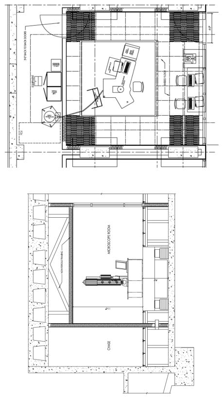
The monochromated, Cs–corrected Zeiss Libra 200-80 TEM is located at the Imaging and Analysis Group in the Center for Nanoscale Systems at Harvard University. The physical location of this microscope is in the Laboratory for Integrated Science and Engineering (LISE) building, which is a specially designed laboratory for nanoscale research comprising imaging, cleanroom and materials research space. The specifications for the design and construction of this facility include isolating instruments from vibration, AC and DC electromagnetic fields, acoustic noise, temperature and humidity fluctuations, HVAC airflow instabilities and involve careful instrument layout. The room is one of a series of ten imaging suites specially designed for high-end imaging equipment. The whole-lab concept of the design and construction of the building was to locate sources of possible interference such as elevators, power distribution systems and conduits away from the sensitive laboratory space.
The LISE building was constructed using steel-reinforced concrete-containing epoxy-coated rebar to minimize possible sources of ground loops within the building structure. The construction of each imaging room is based on a box-within-a-box design, where the ceiling and walls are not directly in physical contact with the building structure (Fig. 1). The entire room is also surrounded on all six sides by welded 5 mm aluminum plate to minimize possible external AC fields. The main source of DC field interference is from the nearby subway system, but this can be compensated by an in-room, active cancellation system if needed. Twisted AC power wiring was used for power distribution throughout the laboratory in rigid metal conduit, with routing of cables away from the microscope column. A chase area behind each of the main microscope rooms provides isolated space for utilities such as water chillers, vacuum pumps, instrument power supplies, Cs-corrector power supplies and computers. In our installation, a set of double walls and double doors keeps noise out of the microscope room, while feed-throughs provide a path for water, power and data connections to the instrument.
Figure 1.
Schematic of the high-resolution electron microscope room design at Harvard University in profile and plan views, showing the separate isolation block, double wall construction and isolated equipment chase.
The microscope itself sits on a separate reinforced concrete block (5 × 12 × 12 ft), surrounded by raised flooring; the whole block was designed to be “floated” should this be required, but vibration measurements made with this block resting on grade show that the noise floor is well within vendor specifications. Acoustic foam panels line the laboratory walls for internal sound absorption and damping. A duct sock distributes airflow into the room, with the airflow returning through perforations in the suspended flooring surrounding the concrete block providing especially laminar airflow. Acoustic curtains across the room on the door side provide an additional measure for both noise and airflow isolation (Muller et al., 2006), and the panels of the curtains are independently adjustable.
Microscope
The Zeiss Libra 200-80 monochromated and Cs-corrected microscope (Fig. 2.) has a Schottky FEG with a maximum accelerating voltage of 200 kV, a third-order CEOS imaging corrector and an in-column Omega filter. The objective lens pole piece has a 5-mm gap with a specified chromatic aberration coefficient Cc of 1.2 mm. The imaging camera is a 4096 X 4096 pixel Gatan UltraScan CCD camera. Significant improvements were made to the standard Zeiss Libra 200 field-emission TEM/STEM platform, which included increased mechanical frame stability, power supply stabilities, and the addition of a second generation Omega-type monochromator and a 2nd order corrected Omega in-column energy filter (Fig. 3). Frame stability was improved by increasing the base width and mounting the entire column on an active air support system. The electron-optics power supplies are stable to the 10−7 or better range.
Figure 2.
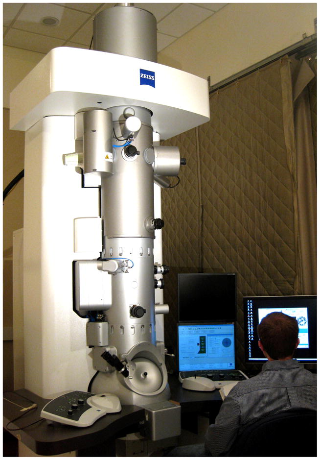
Photograph of the room and the monochromated, Cs-corrected Zeiss Libra 200-80 transmission electron microscope. The room is designed to minimize temperature and airflow changes. Shown in this photograph are the acoustic curtains that isolate the entryway from the room.
Figure 3.
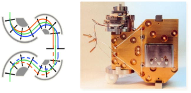
Left: Schematic representation of the Zeiss-CEOS Omega-type electron monochromator. Right: Image of the actual electron monochromator as installed in the Zeiss Libra 200 electron gun (courtesy of M. Haider, CEOS).
The Omega-type monochromator is the only configuration that provides dispersion-free illumination, high brightness (108 A/cm² Sr) with non-distorting optics, as detailed in (Rose, 2009). This design is purely electrostatic and introduces no changes in source magnification during operation and. The beam is deflected in an S-shape and forms an astigmatic image of the virtual source in the selection plane, which is the symmetry plane of the monochromator (Figure 3). There the beam is energy-filtered using an opaque slit, and an array of various slit sizes are available to allow optimization of energy width versus beam current. After leaving the monochromator, the beam is entirely dispersion-free; even the angular dispersion is compensated. It is also possible to switch the monochromator off and operate the microscope with a straight-through beam, as in ordinary operation mode. To take advantage of the reduced energy spread of the monochromator, the microscope also incorporates an in-column energy-loss filter, termed the Omega filter due to its distinct shape (Essers et al., 2010).
The optics of the Omega filter are second-order Cs corrected and third-order optimized, and shows a high transmissivity (Tr = 190 nm2 at 1 eV energy width), and a dispersion of 1.85 μm/eV at 200 kV with excellent isochromaticity in the imaging plane. The filter meets the specified energy resolution of ΔE < 0.2 eV. This energy resolution is routinely achievable in electron-energy-loss spectroscopy (EELS) mode and thus becomes comprable to the energy resolution in X-ray absorption spectroscopy (XAS). This opens up new opportunities to extract highly localized structural information from transition metal oxides with negligible interference from instrumental broadening. In addition to high-energy resolution, the high isochromaticity extends over a large field of view. This feature is necessary for accurate spectrum imaging, where a stack of images is taken with small energy window (at 1 eV). It is also critically important when doing zero-loss, energy-filtered imaging at high magnification. To determine the isochromaticity, the shift of the center of the zero-loss peak was measured over the field of view at a TEM magnification of 16 kX, resulting in an object field of 1.63 × 1.63 μm2. The resulting energy deviation over the field of view was less than 0.14 eV.
The benefit of using a monochromated source and energy filtering for high-resolution imaging is shown by the increase in the cut-off of the temporal-coherence damping envelope resulting from reduced chromatic aberration. Specifically, reducing the source energy distribution (ΔE/E) increases the maximum spatial frequency of the envelope function (the information limit), thus improving the overall resolution, particularly for a Cs corrected instrument. As an example, for a non-monochromated source at 200 kV (ΔE = 0.6 eV) with Cs correction (Cc = 1.2 um, and Cs~0), the theoretical temporal damping envelope limits the PCTF to 83 pm; reducing the energy distribution to ΔE = 0.2 eV for the same parameters improves this limit to 61 pm (Reimer & Kohl, 2008).
Results and Discussion
Spectroscopy results from the electron monochromator are shown in Figure 4, with the non-monochromated source indicating an energy spread at FWHM of 600 meV, which is essentially equivalent to a standard Schottky FEG. Insertion of the 1 μm monochromator slit reduces the energy spread of the electron beam to 81 meV at 200 kV and 62 meV at 80kV, while still leaving sufficient current for usable high-resolution imaging. Slightly better performance is possible by using the 0.5 μm monochromator slit for pure spectroscopy applications. By reducing the voltage of the TEM, there are distinct gains in using electron energy-loss spectroscopy to determine band gaps and the dielectric properties on a nano-meter scale. First, the relativistic losses are reduced. Second, delocalization of the energy-loss signal decreases with the energy of the incident probe. These factors are discussed in detail elsewhere (Stöger-Pollach & Pongratz, 2010).
Figure 4.
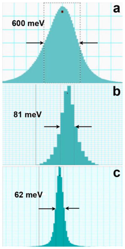
Measured electron source energy spread distributions with: a) non-monochromated beam at 200 kV; b) monochromated beam using the 1 μm slit at 200 kV; and c) monochromated using 1 μm slit width at 80 kV.
To evaluate the information transfer at various accelerating voltages, Young’s interference fringe patterns (Figure 5) were generated from an ultra-thin amorphous tungsten film. The energy spread of the field emission source was reduced by the monochromator to 0.1 eV, and the residual spherical aberration of the objective lens was set to Cs= −1 μm using the integrated Cs corrector. The information limit was 71 pm at 200 kV, which approaches the theoretical limit of 66 pm. The information limit at 80 kV was 93 pm, which is again near the theoretical limit of 88 pm. The resolution at 200 kV was tested using Ge (112), and the resulting images are shown in Figure 6. A line profile through the dumbbell structure is shown in the inset, and indicates that the spacing of 82 pm is well-resolved. To test the resolution of this microscope at lower voltage, a 10-nm-thick single crystal gold (100) sample was imaged at 80 kV, and the result is shown in Figure 7. The inset is a FFT of the image, showing information transferred in the sub-Ångstrom range.
Figure 5.
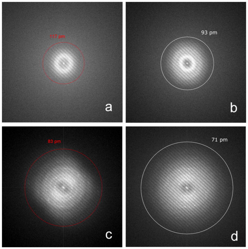
Young’s fringes produced from an ultra-thin tungsten film. All images with Cs correction: a) at 80 kV accelerating voltage without monochromation; b) at 80 kV but with monochromator and energy spread distribution of 0.15 eV; c) at 200 kV with Cs correction but without monochromation; and d) at 200 kV with monochromation with 0.2 eV energy spread, indicating information transfer to 0.071 nm.
Figure 6.
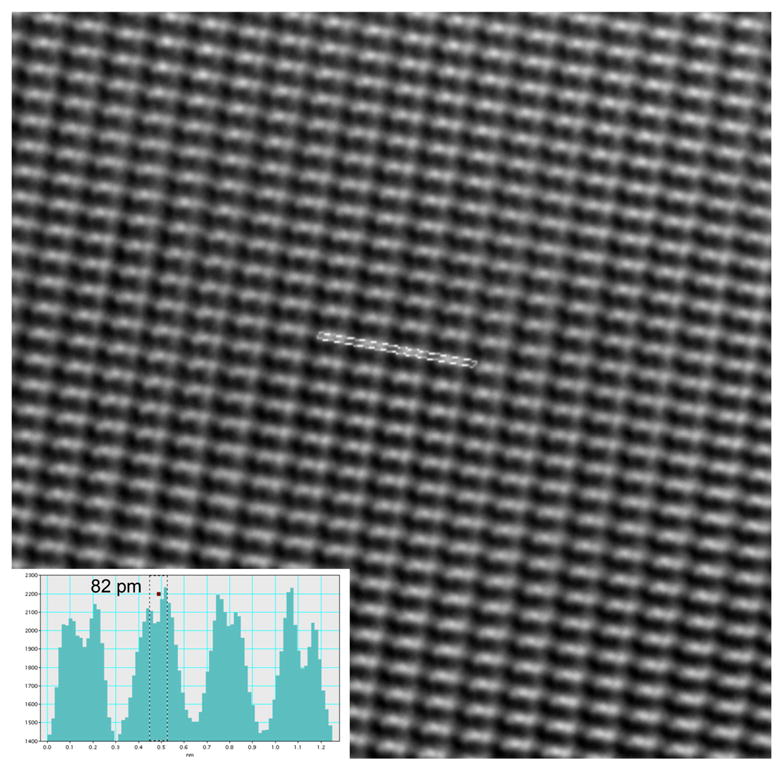
High resolution energy-filtered image of Ge (112) obtained at 200 kV with Cs correction and monochromated beam with 0.1 eV energy spread. Inset, indicated separation of 82pm.
Figure 7.
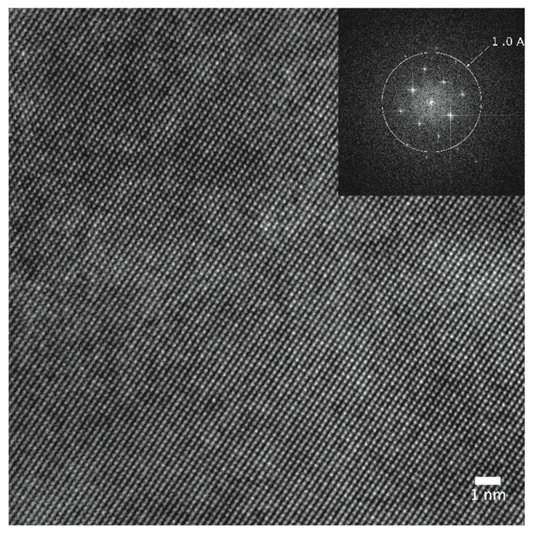
Ultra-thin single crystal gold (100) imaged at 80 kV with Cs-correction and energy monochromation of 0.1 eV. The FFT inset shows information out to beyond 0.1 nm at 80 kV.
Figure 8 shows an image of gold nanoparticle islands on a multi-layer graphene film, which were previously unattainable at energies above 86 keV due to knock-on damage of the graphene substrate (Smith & Luzzi, 2001). This sample was produced by depositing gold colloids (EM.GC5 from BBI International) from solution to the surface of mechanically exfoliated graphene layers from a highly ordered pyrolytic graphite source, following the method outlined in (Bell et al., 2009). Close examination of the images shows the underlying graphene film. Imaging such structures without damaging the graphene substrate may allow a new understanding of how the substrate interacts with the Au nanoclusters (van Huis et al., 2009; Girit et al., 2009). To obtain this image at 80 kV, the monochromator was adjusted to produce an energy spread of ΔE = 0.1 eV, with the Cs = −1.2 μm.
Figure 8.
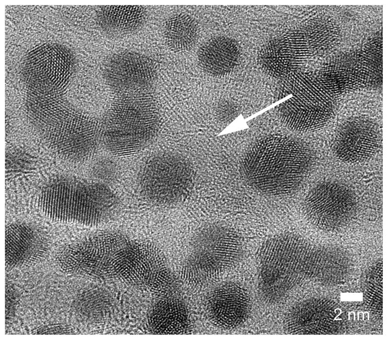
Gold nanoparticle islands on multi-layer graphene film imaged with electron monochromation (ΔE = 0.1 eV) with Cs correction of – 1.2 μm and accelerating voltage of 80 kV. The Au fringes and the underlying graphene structure are clearly visible in the indicated areas between the nanoparticles.
Another example of atomic resolution at 80 kV is shown in Figure 9. The sample is a cluster of single-wall carbon nanotubes suspended over a hole in a carbon membrane. The image clearly shows the carbon atom arrangements in the sidewalls of the nanotubes (Suenaga et al., 2007). Such images would not be possible without the reduced damage and the Ångstrom resolution of the Cs/MC instrument operating at 80 kV. This image was obtained using zero-loss energy filtering at 80 kV with Cs correction and a monochromator slit width of 4 μm.
Figure 9.
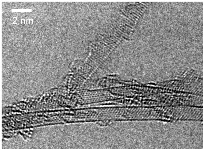
Single wall carbon nanotubes imaged at 80 kV with Cs correction, a monochromator slit width of 4 um, and zero-loss imaging.
Summary
Sub-Ångstrom, low-voltage Transmission Electron Microscopy is now a practical reality. Monochromation with Cs correction yields a further step along the path to improving electron microscope resolution and analytical capability. We have evaluated the performance and application of the Zeiss Libra 200-80 Cs corrected and monochromated microscope on suitable evaluation samples including gold, germanium, graphene and carbon nanotubes. The results demonstrate information limits very close to theoretical values for both 200 and 80 keV operation, and show that imaging single atoms with Ångstrom resolution at 80 keV is possible on this newly constructed instrument. By employing an Omega-type functional monochromator, expansion of the temporal envelope of the phase contrast transfer function to reduce the ΔE is a direct benefit that leads to improved resolution. Finally, we have demonstrated that a monochromated and Cs-corrected transmission electron microscope operating at 80 kV accelerating voltage shows information transfer better than one Ångstrom.
Acknowledgments
The authors thank Prof. Max Haider and the team at CEOS GmbH, Heidelberg Germany, for their assistance with preparing this paper. We acknowledge the efforts of Stephan Myer, Alexander Orchowski, Dimitry Kolmykov of Carl Zeiss NTS GmbH and Payam Tayebati of Carl Zeiss SMT during instrument installation and testing, and thank Prof. Jene Golovchenko and Prof. Frans Spaepen for many helpful discussions during preparation of this manuscript. This work was performed in part at the Center for Nanoscale Systems, Harvard University, a member of the National Nanotechnology Infrastructure Network, which is supported by the National Science Foundation under award no. ECS-0335765. CJR acknowledges support from the National Human Genome Research Institute, The National Institutes of Health under award no. 5R01HG003703.
References
- Bell DC, Lemme MC, Stern LA, Williams JR, Marcus CM. Precision cutting and patterning of graphene with helium ions. Nanotechnology. 2009;20:455301. doi: 10.1088/0957-4484/20/45/455301. [DOI] [PubMed] [Google Scholar]
- Dahmen U, Erni R, Radmilovic V, Ksielowski C, Rossell MD, Denes P. Background, status and future of the Transmission Electron Aberration-corrected Microscope project. Phil Trans R Soc A. 2009;367:3795–3808. doi: 10.1098/rsta.2009.0094. [DOI] [PubMed] [Google Scholar]
- Essers E, Benner G, Mandler T, Meyer S, Mittmann D, Schnell M, Höschen R. Energy resolution of an Omega-type monochromator and imaging properties of the MANDOLINE filter. Ultramicroscopy. 2010 in press. [Google Scholar]
- Girit ÇÖ, Meyer JC, Erni R, Rossell MD, Ksielowski C, Yang L, Park CH, Crommie MF, Cohen ML, Louie SG, Zettl A. Graphene at the Edge: Stability and Dynamics. Science. 2009;323:1705–1708. doi: 10.1126/science.1166999. [DOI] [PubMed] [Google Scholar]
- Haider M, Schwan E. Correction of the spherical aberration of a 200 kV TEM by means of a hexapole-corrector. Optik. 1995;99:167–179. [Google Scholar]
- Haider M, Uhlemann S, Schwan E, Rose H, Kabius B, Urban K. Electron microscopy image enhanced. Nature. 1998;392:768–769. [Google Scholar]
- Hawkes PW. Aberration-Corrected Electron Microscopy, Advances in Imaging and Electron Physics. Elsevier; 2008. p. 153. [Google Scholar]
- Hawkes PW, Spence JCH. Science of Microscopy. Springer; New York: 2007. [Google Scholar]
- Meyer JC, Chuvilin A, Algara-Siller G, Biskupek J, Kaiser U. Selective Sputtering and Atomic Resolution Imaging of Atomically Thin Boron Nitride Membranes. Nano Lett. 2009;9:2683–2689. doi: 10.1021/nl9011497. [DOI] [PubMed] [Google Scholar]
- Muller DA, Kirkland EJ, Thomas MG, Grazul JL, Fitting L, Weyland M. Room design for high-performance electron microscopy. Ultramicroscopy. 2006;106:11–12. doi: 10.1016/j.ultramic.2006.04.017. [DOI] [PubMed] [Google Scholar]
- van Huis MA, Young NP, Pandraud G, Creemer JF, Vanmaekelbergh D, Kirkland AI, Zandbergen HW. Atomic Imaging of Phase Transitions and Morphology Transformations in Nanocrystals. Advanced Materials. 2009;21:4992–4995. doi: 10.1002/adma.200902561. [DOI] [PubMed] [Google Scholar]
- Reimer L, Kohl H. Transmission Electron Microscopy: Physics of Imaging Formation. 5. Springer; Berlin Heidelberg: 2008. [Google Scholar]
- Rose H. Geometrical Charged Particle Optics. Springer; Berlin Heidelberg: 2009. [Google Scholar]
- Smith BW, Luzzi DE. Electron irradiation effects in single wall carbon Nanotubes. J Appl Phys. 2001;90:3509–3515. [Google Scholar]
- Stöger-Pollach M, Pongratz P. Advantages of low beam energies in a TEM for valence EELS. Journal of Physics Conference Series 209; 16th International Conference on Microscopy of Semiconducting Materials; 2010. p. 012031. [Google Scholar]
- Suenaga K, Wakabayashi H, Koshino M, Sato Y, Urita K, Iijima S. Imaging active topological defects in carbon nanotubes. Nature Nanotech. 2007;2:358–360. doi: 10.1038/nnano.2007.141. [DOI] [PubMed] [Google Scholar]


