Abstract
We demonstrate lensless fluorescent microscopy over a large field-of-view of ~60 mm2 with a spatial resolution of <4 μm. In this on-chip fluorescent imaging modality, the samples are placed on a fiber-optic faceplate that is tapered such that the density of the fiber-optic waveguides on the top facet is >5 fold larger than the bottom one. Placed on this tapered faceplate, the fluorescent samples are pumped from the side through a glass hemisphere interface. After excitation of the samples, the pump light is rejected through total internal reflection that occurs at the bottom facet of the sample substrate. The fluorescent emission from the sample is then collected by the smaller end of the tapered faceplate and is delivered to an opto-electronic sensor-array to be digitally sampled. Using a compressive sampling algorithm, we decode these raw lensfree images to validate the resolution (<4 μm) of this on-chip fluorescent imaging platform using microparticles as well as labeled Giardia muris cysts. This wide-field lensfree fluorescent microscopy platform, being compact and high-throughput, might provide a valuable tool especially for cytometry, rare cell analysis (involving large area microfluidic systems) as well as for microarray imaging applications.
Introduction
With the recent advances in opto-electronic components as well as computational resources having better processors and more sophisticated algorithms, lensfree on-chip imaging is becoming an important alternative to conventional lens-based microscopy for both bright-field and fluorescent imaging.1–10 Lensfree imaging in general aims to replace bulky and expensive optical components with much more compact and cost-effective alternatives, and could provide a useful platform especially for microscopic analysis of microfluidic systems. In addition to the simplicity and compactness of its architecture,5,7 lensfree imaging also provides a throughput advantage such that it permits a significantly larger imaging field-of-view (FOV). As an example, we have recently demonstrated a lensfree fluorescent imaging platform that can achieve ~10 μm resolution over >8 cm2 FOV.10 While its resolution is modest, such a large imaging FOV is rather valuable for high-throughput cytometry and rare cell detection applications that demand imaging of large area microfluidic channels.11,12
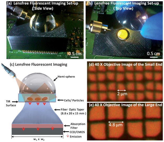
In this work, we improve the spatial resolution of our lensfree fluorescent imaging modality to achieve <4 μm resolution over an FOV of ~60 mm2 without affecting the compactness and the simplicity of the on-chip imager. In this lensfree fluorescent imaging modality, the sample chip is placed onto a tapered fiber-optic faceplate that has ~5 fold higher density of fiber-optic waveguides on its top facet compared to the bottom one (see Fig. 1). This compact taper geometry samples the fluorescent emission from the objects with a period of ~2 μm and achieves ~2.4 fold magnification of the lensfree fluorescent patterns over ~60 mm2 FOV without introducing any spatial aberrations into the lensfree imaging system. To excite the fluorescent samples located on the tapered faceplate, an incoherent source is coupled to this system through a glass hemisphere as illustrated in Fig. 1. After interacting with the fluorescent objects that are placed within a microfluidic channel, the pump is rejected through total internal reflection occurring at the bottom facet of the micro-fluidic chip (see Fig. 1). Note that this configuration should not be confused with conventional Total Internal Reflection Fluorescent (TIRF) microscopy systems13,14 since in our geometry the excitation occurs through travelling waves rather than evanescent waves, and therefore a much large sample volume can be pumped all in parallel using our approach.
Fig. 1.
(a and b) Pictures of the experimental set-up are shown. (c) The schematic diagram of the lensfree fluorescent on-chip imaging platform is illustrated. (d and e) Microscopic images of the top and bottom facets of the fiber-optic taper are shown. w1 = 25 mm and w2 = 35 mm are used in this work.
With further removal of the weakly scattered excitation light by using an inexpensive absorption filter (Fig. 1), a sufficiently strong dark-field background is created such that the fluorescent emission from the objects can be sampled using an opto-electronic sensor-array (e.g., a charge-coupled-device—CCD). After acquisition of these raw lensfree fluorescent images, a compressive sampling based decoding algorithm10,15–17 is then used to partially undo the effect of diffraction such that a lensfree spatial resolution of <4 μm can be achieved over the entire faceplate taper area (~60 mm2). We should emphasize that, without a trade-off in spatial resolution, this FOV can further be increased by using larger area CCD chips within the same lens-free imaging architecture shown in Fig. 1.
This compact lensfree fluorescent on-chip imager, with a decent spatial resolution and an ultra-wide FOV could especially be valuable for high-throughput cytometry and rare cell analysis involving large area microfluidic systems, as well as for microarray imaging applications.
Results and discussion
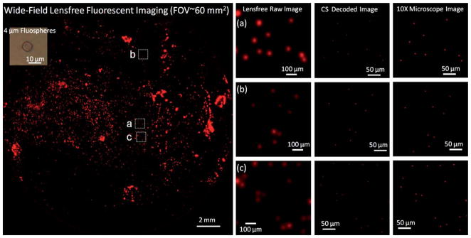
The presented lensfree on-chip microscopy platform is composed of a CCD sensor chip, a thin absorption filter, a tapered fiber-optic faceplate and a glass hemisphere (see Fig. 1). We tested the performance of this on-chip microscopy platform by imaging 4 and 2 μm diameter fluorescent particles as well as Giardia muris cysts. In Fig. 2, an imaging FOV of ~60 mm2 is illustrated, with three digitally zoomed sections showing the raw lensfree signatures of the fluorescent particles. These raw fluorescent images reflect the lensfree signal detected at the CCD chip, and are then decoded using a compressive sampling (CS) algorithm10,17 to yield images of the object plane with improved spatial resolution as demonstrated in Fig. 2 (refer to the Experimental Methods Section for further details). The same figure also shows 10× microscope-objective (0.25 Numerical Aperture—NA) images of the same objects for comparison purposes, which very well agree with our lensfree imaging results.
Fig. 2.
(Left) the entire imaging FOV (~60 mm2) of the lensfree fluorescent microscope shown in Fig. 1 is illustrated. (a–c) Three different zoomed sections of the lensfree fluorescent image are shown. The middle column in (a–c) illustrates the compressive sampling (CS) decoder results, whereas the right column shows (for comparison purposes) images of the same microparticles (4 μm diameter) using a conventional lens-based fluorescent microscope (10× objective lens, NA = 0.25). The CS decoder uses the raw lensfree fluorescent images which are shown in the left column of (a–c). The images are pseudo-colored in red.
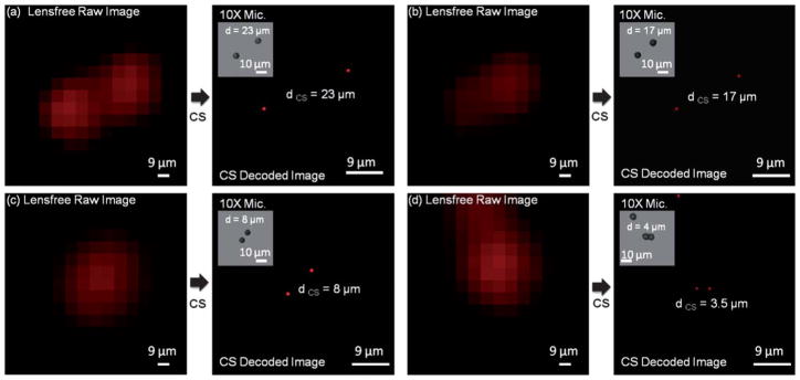
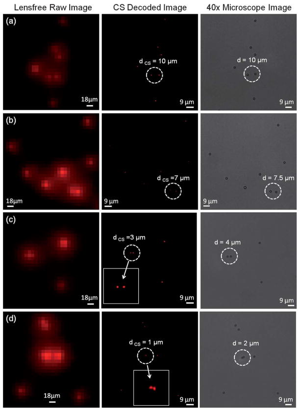
To quantify our resolution, in Fig. 3 and 4 we focus on smaller regions of interest where the fluorescent particles (4 and 2 μm diameter) were close to each other. Fig. 3 and 4 also illustrate bright-field microscope images of these fluorescent particles which act as our references in terms of the distances (d) between particles. We also show in these figures the raw lensfree fluorescent images (which are pixelated) for the same particles as well as their CS decoded versions to validate our resolution. Note that unlike conventional lens-based microscopy, objects separated by <15 μm partially overlap with each other at the detector plane due to unavoidable diffraction occurring in this lensfree platform. Our CS decoding results shown in Fig. 3 and 4 demonstrate that we can resolve closely spaced fluorescent particles from each other, achieving a lensfree spatial resolution of <4 μm. Considering that the pixel size at the CCD chip of this lensfree on-chip imager is 9 μm, a resolution of <4 μm is quite significant.
Fig. 3.
Resolution of our lensfree fluorescent on-chip microscope is quantified using 4 μm diameter particles. The pixelated raw lensfree fluorescent images are decoded using a compressive sampling (CS) algorithm to resolve the overlapping lensfree fluorescent emission patterns arising from the particles. The inset images in each decoded image illustrate (for comparison purposes) bright-field microscope images of the same microparticles. Note that because the samples were sequentially imaged using the microscope after their lensfree images were acquired, their relative orientations might be slightly rotated/shifted between the two imaging modalities. The lensfree images are pseudo-colored in red.
Fig. 4.
Resolution of our lensfree fluorescent on-chip microscope is quantified using 2 μm diameter particles. The pixelated raw lensfree fluorescent images are decoded using a CS algorithm to resolve the overlapping lensfree fluorescent emission patterns arising from the particles. For comparison purposes conventional bright-field microscope images of the same 2 μm diameter particles are also shown on the right column. Note that because the samples were sequentially imaged using the microscope after their lensfree images were acquired, their relative orientations might be slightly rotated/shifted between the two imaging modalities. The lensfree images are pseudo-colored in red.
We have also validated the performance of our lensfree fluorescent microscopy platform by imaging labeled Giardia muris cysts as illustrated in Fig. 5. When combined with its large FOV within a compact on-chip platform, these results could be especially important for rapid screening of water-borne parasites in field settings.
Fig. 5.
Lensfree fluorescent imaging results for Giardia muris cysts are shown. A conventional microscope image of the same FOV is also illustrated in (c). Note that because the samples were sequentially imaged using the microscope after their lensfree images were acquired, their relative orientations might be slightly rotated/shifted between the two imaging modalities. The lensfree images are pseudo-colored in red.
The function of the tapered fiber-optic faceplate in our lensless geometry is that the fluorescent emission of the objects is sampled with a dense grid of optical waveguides (~2 μm period) and is delivered to the CCD sensor with a larger grid (~4.8 μm period) such that the relative distances in the object plane are roughly magnified by ~2.4×. While this magnification is an important parameter for spatial resolution, there are other factors that significantly affect the achievable resolution in our platform:
Detection Signal-to-Noise Ratio (SNR)
This parameter is governed by several factors, ranging from noise floor of the sensor, faceplate-to-sensor and object-to-faceplate distances, the numerical aperture of the faceplate, as well as the emission intensity of the objects and the strength of the dark-field background. In principle, if the SNR of the raw fluorescent images is very high, the resolution of the compressively decoded images can become independent of the magnification of the faceplate taper, and can in theory approach sub-micron levels. Therefore, active cooling of the opto-electronic sensor array is an important route that we can utilize to further improve our lensfree resolution without a trade-off in our imaging FOV. The fact that the thickness of the faceplate is >1–2 cm can also thermally isolate the samples from the sensor chip, helping to implement active cooling of the sensor without a damage to the samples. Such an increased digital SNR would also increase the detection numerical aperture of our platform, such that more of the oblique fluorescent rays can now be detected above the noise floor of the sensor. Therefore under improved SNR levels, our detection numerical aperture will be ultimately limited by the numerical aperture of the fiber-optic faceplate, which in our experimental set-up was ~1.
Other key parameters that set the detection SNR are the faceplate-to-sensor and object-to-faceplate distances. The object-to-faceplate vertical distance can be reduced to ~10 to 20 μm. However, the faceplate-to-sensor vertical distance will have to be limited with the thickness of the absorption filter which can get as small as ~20 to 30 μm (see Fig. 1). One other key parameter that will directly determine the detection SNR in our lensfree imaging geometry is the fluorescent emission intensity of the samples (compared to the background) which is mostly determined by the quantum efficiency of labeling dyes, excitation power and wavelength, as well as the labeling efficiency of the sample.
Therefore, governed by the above discussed parameters, the digital SNR of our lensfree images is one of the most important factors that influence the spatial resolution of our fluorescent on-chip imager, which can potentially achieve sub-micron resolution by additional systematic improvements in our optical set-up.
Lensfree Point-Spread Function (PSF)
We define the lensfree PSF of our on-chip imaging system as the 2D spatial function that represents the fluorescent emission pattern of a point source located at the object plane, before being sampled by the sensor chip at the detector plane. As for the discussion of the system PSF and its effect on spatial resolution one has to be careful. Under a strong detection SNR and a large pixel size at the sensor chip (as we typically employ, e.g., ~9 μm), the narrowest lensfree PSF is not necessarily the best route for improving CS decoded resolution. To better understand this argument, assume that the spatial width of the lensfree PSF is hypothetically made smaller than the large pixel size at the sensor chip. In this case, two fluorescent points that are close to each other at the sub-pixel level would both contribute to a single pixel, which makes it impossible to resolve them no matter what type of digital decoder is used. Simply put, infinitely many different combinations of these two point sources within the same pixel would yield the same signal, making decoding at the sub-pixel level physically impossible.
However, for the same pixel size and digital SNR at the sensor chip, if this time the width of the lensfree PSF is increased (which could be achieved by e.g., slightly increasing the vertical distance of the object plane from the sensor surface), then decoding of these sub-pixel separated objects would be feasible since several different pixels (dictated by the practical width of the PSF) can now detect weighted sums of these two closely spaced point sources. This conclusion is true as long as the detection SNR does not degrade significantly (getting close to the noise floor of the sensor) due to spatial broadening.
In other words, for a given large pixel size at the sensor chip, after a certain PSF width is reached, a further increase in its width might start to practically reduce the detection SNR due to signal spreading, and this would set the boundary for the optimum PSF, which is entirely dictated by the pixel size at the sensor chip and the noise performance of lensfree platform. Note also that since we are employing a compressive decoder, defining an optimum PSF width for a given pixel size based on the classical Nyquist sampling theorem would also be misleading, especially for spatially sparse fluorescent objects. More formal treatment of this topic is provided in ref. 10, through mathematical analysis of compressive sampling and its relationship to lensfree on-chip fluorescent imaging.
The main function of the fiber-optic faceplate in lensfree fluorescent on-chip imaging can also be understood from the perspective of PSF engineering, i.e., for a given pixel size at the sensor chip, through the use of a faceplate, an optimum PSF can be created. In principle, a larger magnification fiber-optic taper could potentially be used for getting a better spatial resolution with our lensfree on-chip imaging platform (assuming that a decent SNR could also be achieved). However, as the diameter of the fiber-cores gets smaller and smaller the cross-talk among individual fiber-optic waveguides within the tapered faceplate structure would start to increase which could degrade the imaging quality of our platform, unless the refractive index of the core regions is increased to reduce this modal cross-talk.
Tapering of the faceplate as shown in Fig. 1 adds another advantage to our on-chip platform through image magnification such that more pixels can now detect the lensfree emission of the objects without sacrificing the detection SNR or without introducing spatial aberrations within the large imaging FOV. In addition to these, another valuable function of the fiber-optic faceplate in lensfree on-chip fluorescent imaging is thermal isolation of the objects from the sensor chip and the reader circuit such that operating temperatures within the sample micro-channel can be better controlled.
We believe that such a compact and light-weight lensfree fluorescent microscopy platform (Fig. 1), with rapid compressive decoding algorithms behind it, could be quite useful for high-throughput screening applications, rare cell analysis and for microarray imaging applications.
Experimental methods
Design of the wide-field lensfree fluorescent microscopy platform using a tapered fiber-optic faceplate
Our lensfree on-chip fluorescent microscopy platform is built on an 11 MPixel CCD sensor chip (KODAK, KAI-11002, 9 μm pixel size), which was operated at room temperature. A thin absorption filter with dyes is fabricated by coating 30 μm thick glass substrates. This fabrication process starts with dissolving Orasol dyes in cyclopentanone solvent and adding KMPR 1005 Photoresist (~0.4 g mL−1 dye concentration), after which the excess dye material in the mixture is removed using a 0.45 μm diameter porous filter. The raw solution is then processed by spin coating for 20 s at 2000 rpm, baking for 300 s at 100 °C, flood exposure at 13 mW cm−2 for 35 s, and finally baking for another 120 s at 100 °C. One of these fabricated filters is gently placed on the sensor array with a vacuum pen. Then the tapered fiber-optic faceplate (Edmund Optics, NT55-134, numerical aperture: 1.0, size ratio: 18:8 mm) is placed onto this absorption filter, with the large facet facing the sensor chip as shown in Fig. 1. A 3D printer is used to create a customized housing to cover the optical components, except the top facet of the taper (see Fig. 1b). Blocking unwanted light is important to decrease the leakage from excitation or ambient light, which can decrease the image contrast otherwise. As for the excitation, the illumination was provided by a xenon lamp coupled to a monochromator such that the center wavelength was chosen as 580 nm with ~15 nm bandwidth. The illumination angle was adjusted by using a multi-mode fiber-optic cable attached to a mechanical holder, so that total-internal reflection can be satisfied over the entire imaging area (~60 mm2). The fluorescent samples are then placed onto the smaller facet of the tapered faceplate. And finally, a glass hemisphere is assembled to couple the excitation light to the samples using an index-matching gel (see Fig. 1). The lensfree fluorescent images are then recorded using a custom developed Labview interface, typically within 2–3 seconds of exposure time.
Fluorescent sample preparation
Fluorescent beads with 4 μm and 2 μm diameters (red beads: excitation 580 nm/emission 605 nm) were purchased from Invitrogen (Carlsbad, CA). The stock solution is diluted 4000 times with DI water in small aliquots. Then using a micropipette, the bead solution (~10 μL) is transferred onto a disposable glass substrate (thickness: ~30 to 100 μm) and is sandwiched using another glass substrate before being imaged using our lensfree on-chip microscope.
Giardia muris cysts were purchased from Waterborne Inc. (New Orleans, LA, USA). The stock solution of these cysts has a concentration of ~5 × 10⁶ parasites mL−1. To avoid the dynamic motion of the parasites, they were fixed in 5% formalin/PBS at pH 7.4/0.01% Tween-20. A small amount of this solution (e.g. 100–200 μL) was centrifuged and re-suspended in the form of PBS suspension. As for the labeling dye, 1 mM SYTO®64 nucleic acid dye was used with the mixing ratio of 5 μL of dye and 100 μL parasite-consisting suspensions. Once prepared, this mixture was incubated in dark environment for ~30 min. Just after activation of dye labeling within the parasite body (emission peak wavelength: 619 nm), the unbound dyes (which might potentially introduce unwanted background) were removed by another centrifuging and re-suspension in PBS. The final sample solution was then placed between two glass slides for wide-field lensfree imaging on a chip.
Compressive sampling based decoding of raw lensfree fluorescent images
We made use of compressive sampling based decoding to partially undo the effect of diffraction, which is an inherent result of lensfree on-chip operation. In this method, we first measure the point-spread-function of the lensfreee imaging system using small fluorescent particles (e.g., ~2 μm diameter). For this end, several lensfree fluorescent spots of isolated particles are aligned with respect to each other and are then averaged to yield the lensfree fluorescent point-spread-function of the platform. Based on this, for any arbitrary distribution of fluorescent point sources at the object plane, one can calculate the expected lensfree fluorescent pattern that is to be sampled at the detector plane. We should note that we can also measure the individual point-spread functions corresponding to different vertical layers, and use this information to calculate the expected lensfree fluorescent pattern at the detector array for e.g., a 3D stack of fluorescent objects.
To decode a given lensfree fluorescent image (whether from a single layer or multiple vertical layers), we iteratively minimize (using truncated Newton interior-point method17) a cost function that is defined by l1-regularized least square error between the calculated (i.e., expected) lensfree fluorescent pattern and the measured one at the detector array.10 This entire optimization process is based on sparsity of the fluorescent distribution at the object plane and it typically converges after ~40 to 60 iterations taking ~0.5 to 2 minutes for e.g., the regions of interest shown in Fig. 3 using a 3.2 GHz processor (Intel Core(™) i5 CPU 650). As a result of this compressive decoding process, the resolving power of our lensfree imaging platform significantly increases achieving <4 μm resolution over a wide field-of-view of ~60 mm2.
Conclusions
In conclusion, we have demonstrated a lensfree fluorescent on-chip microscopy platform that can image labeled cells/particles over an FOV of ~60 mm2 with <4 μm spatial resolution. This lensfree fluorescent microscope is based on a compact fiber-optic faceplate taper as well as a compressive sampling algorithm that can quickly decode the raw lensfree fluorescent patterns detected at the sensor, digitally creating higher resolution images of the fluorescent objects on the chip. This compact lensfree fluorescent microscope, with a decent spatial resolution and an ultra-wide FOV, could especially be valuable for high-throughput cytometry, rare cell analysis within large area microfluidic chips, and for microarray imaging applications.
Acknowledgments
A. Ozcan gratefully acknowledges the support of NSF CAREER Award on BioPhotonics, the Office of Naval Research (ONR) under the Young Investigator Award 2009 and the NIH Director’s New Innovator Award—Award Number DP2OD006427 from the Office of The Director, National Institutes of Health. The authors also acknowledge the support of the Okawa Foundation, Vodafone Americas Foundation, DARPA DSO (under 56556-MS-DRP), and NSF BISH program (under Awards # 0754880 and 0930501).
Biography

Dr. Aydogan Ozcan received his Ph.D. degree at Stanford University Electrical Engineering (EE) Department. He joined UCLA in 2007 as an Assistant Professor of EE, where he is currently leading the Bio-Photonics Laboratory. He holds 17 issued patents and another 8 pending patent applications and is also the author of one book and the co-author of more than 150 peer-reviewed articles in major journals and conferences. Prof. Ozcan received various awards including NSF CAREER Award, NIH Director’s New Innovator Award, ONR Young Investigator Award, IEEE Photonics Society Young Investigator Award, MIT’s TR35 Award, National Geographic Emerging Explorer Award, etc.
Footnotes
This article is part of a themed issue on Emerging Investigators.
References
- 1.Haddad WS, Cullen D, Solem JC, Longworth JW, McPherson A, Boyer K, Rhodes CK. Appl Opt. 1992;31:4973–4978. doi: 10.1364/AO.31.004973. [DOI] [PubMed] [Google Scholar]
- 2.Xu W, Jericho MH, Meinertzhagen IA, Kreuzer HJ. Proc Natl Acad Sci U S A. 2001;98:11301–11305. doi: 10.1073/pnas.191361398. [DOI] [PMC free article] [PubMed] [Google Scholar]
- 3.Pedrini G, Tiziani HJ. Appl Opt. 2002;41:4489–4496. doi: 10.1364/ao.41.004489. [DOI] [PubMed] [Google Scholar]
- 4.Repetto L, Piano E, Pontiggia C. Opt Lett. 2004;29:1132–1134. doi: 10.1364/ol.29.001132. [DOI] [PubMed] [Google Scholar]
- 5.Mudanyali O, Tseng D, Oh C, Isikman SO, Sencan I, Bishara W, Oztoprak C, Seo S, Khademhosseini B, Ozcan A. Lab Chip. 2010;10:1417–1428. doi: 10.1039/c000453g. [DOI] [PMC free article] [PubMed] [Google Scholar]
- 6.Bishara W, Su T, Coskun AF, Ozcan A. Opt Express. 2010;18(11):11181–11191. doi: 10.1364/OE.18.011181. [DOI] [PMC free article] [PubMed] [Google Scholar]
- 7.Tseng D, Mudanyali O, Oztoprak C, Isikman SO, Sencan I, Yaglidere O, Ozcan A. Lab Chip. 2010;10:1787–1792. doi: 10.1039/c003477k. [DOI] [PMC free article] [PubMed] [Google Scholar]
- 8.Heng X, Erickson D, Baugh LR, Yaqoob Z, Sternberg PW, Psaltis D, Yang C. Lab Chip. 2006;6:1274–1276. doi: 10.1039/b604676b. [DOI] [PubMed] [Google Scholar]
- 9.Coskun AF, Su T, Ozcan A. Lab Chip. 2010;10:824–827. doi: 10.1039/b926561a. [DOI] [PMC free article] [PubMed] [Google Scholar]
- 10.Coskun AF, Sencan I, Su T, Ozcan A. Opt Express. 2010;18:10510–10523. doi: 10.1364/OE.18.010510. [DOI] [PMC free article] [PubMed] [Google Scholar]
- 11.Nagrath S, Sequist LV, Maheswaran S, Bell DW, Irimia D, Ulkus L, Smith MR, Kwak EL, Digumarthy S, Muzikansky A, Ryan P, Balis UJ, Tompkins RG, Haber DA, Toner M. Nature. 2007;450:1235–1239. doi: 10.1038/nature06385. [DOI] [PMC free article] [PubMed] [Google Scholar]
- 12.Stott SL, Hsu C, Tsukrov DI, Yu M, Miyamoto DT, Waltman BA, Rothenberg SM, Shah AM, Smas ME, Korir GK, Floyd FP, Gilman AJ, Lord JB, Winokur D, Springer S, Irimia D, Nagrath S, Sequist LV, Lee RJ, Isselbacher KJ, Maheswaran S, Haber DA, Toner M. Proc Natl Acad Sci U S A. 2010;107:18392–18397. doi: 10.1073/pnas.1012539107. [DOI] [PMC free article] [PubMed] [Google Scholar]
- 13.Schneckenburger H. Curr Opin Biotechnol. 2005;16:13–18. doi: 10.1016/j.copbio.2004.12.004. [DOI] [PubMed] [Google Scholar]
- 14.Roy SR, Hohng S, Ha T. Nat Methods. 2008;5:507–516. doi: 10.1038/nmeth.1208. [DOI] [PMC free article] [PubMed] [Google Scholar]
- 15.Candes EJ, Tao T. IEEE Trans Inform Theory. 2006;52:5406–5425. [Google Scholar]
- 16.Donoho DL. IEEE Trans Inform Theory. 2006;52:1289–1306. [Google Scholar]
- 17.Kim SJ, Koh K, Lustig M, Boyd S, Gorinevsky D. IEEE J Sel Top Signal Process. 2007;1:606–617. [Google Scholar]


