Abstract
There is strong experimental evidence for the existence of strange modes of failure of microelectromechanical systems (MEMS) devices under mechanical shock and impact. Such failures have not been explained with conventional models of MEMS. These failures are characterized by overlaps between moving microstructures and stationary electrodes, which cause electrical shorts. This work presents modeling and simulation of MEMS devices under the combination of shock loads and electrostatic actuation, which sheds light on the influence of these forces on the pull-in instability. Our results indicate that the reported strange failures can be attributed to early dynamic pull-in instability. The results show that the combination of a shock load and an electrostatic actuation makes the instability threshold much lower than the threshold predicted, considering the effect of shock alone or electrostatic actuation alone. In this work, a single-degree-of-freedom model is utilized to investigate the effect of the shock–electrostatic interaction on the response of MEMS devices. Then, a reduced-order model is used to demonstrate the effect of this interaction on MEMS devices employing cantilever and clamped–clamped microbeams. The results of the reduced-order model are verified by comparing with finite-element predictions. It is shown that the shock–electrostatic interaction can be used to design smart MEMS switches triggered at a predetermined level of shock and acceleration.
1. Introduction and background
The technology of microelectromechanical systems (MEMS) is now rapidly maturing and many MEMS devices are commercialized or ready for marketing. Currently, the commercialization of MEMS is a major focus for engineers. One of the most critical issues affecting the commercialization of MEMS devices is their reliability under mechanical shock and impact. Hence, there are increasing demands to improve the design of MEMS to withstand shock loads. MEMS can be exposed to shock during fabrication, deployment and operation. Examples of such conditions are dynamic loading in space applications and harsh environments in military applications [1]. Further, a crucial criterion for automotive and industrial applications is the survivability of portable devices containing MEMS when dropped on hard surfaces [2], which can induce significant shock loads. Such highly dynamic loads may lead to various damage mechanisms, such as forming of cracks and chipping of small fragments. In MEMS, shock loads can cause microstructures, such as suspended microbeams, to hit the stationary electrodes underneath them causing stiction [3] and short circuit problems [4], and hence failure in the device’s function. Unlike failure in large devices, failure in MEMS does not have to mean fracture of structures due to high stresses; it can occur through stiction and electric short circuits due to contacts between movable and stationary electrodes.
MEMS devices typically employ capacitive sensing and/or actuation, in which one plate or electrode is actuated electrostatically and its motion is detected by capacitive changes. There are numerous examples of MEMS devices, which rely on electrostatic excitation and detection, such as comb-drive actuators, resonant microsensors and RF MEMS switches. In this method, the driving load is simply the attractive force between two electrodes of a capacitor. The electrostatic load has an upper limit beyond which the mechanical restoring force of the structure can no longer resist its opposing electrostatic force, thereby leading to the collapse of the structure. This structural instability phenomenon is known as pull-in. A key aim in the design of many MEMS devices is to tune the electrostatic load away from the pull-in instability in order to avoid failure of the devices.
Many studies have addressed the pull-in phenomenon and presented tools to predict its occurrence so that designers can avoid it. Some studies predicted pull-in based on static analysis, which accounts for the dc electrostatic force and the elastic resorting forces of the microstructure [5–7]. Others have, in addition, accounted for the transient motion of microstructures, which lead to a dynamic pull-in. This dynamic instability can take place below the predicted static instability limit. The dynamic pull-in phenomenon was reported and analyzed for switches actuated by a step voltage [8, 9]. These studies indicate that the dynamic pull-in voltage can be as low as 92% of the static pull-in voltage. In the case of ac harmonic excitation, dynamic pull-in was found to be below 50% of the static pull-in voltage [10]. These studies raise the possibility that under the combination of electrostatic and mechanical shock or impact load, dynamic pull-in may be triggered at even lower values of the applied voltage.
The reliability of MEMS when exposed to shock and impact has been a subject of increasing interest in recent years. Béliveau et al [11] characterized experimentally the response of commercial accelerometers due to shock loads and observed some unexpected responses. Brown and Davis [12] and Brown et al [13] subjected commercial accelerometers and a pressure sensor to high-g tests. They reported peculiar modes of failure under severe shock conditions and concluded that improved dynamic modeling and characterization of MEMS devices under shock load are needed. Li and Shemansky [14] studied the motion of MEMS accelerometers during drop tests. They used a single-degree-of-freedom (SDOF) model and a continuous system beam model to account for the flexibility of the structures and calculated their maximum deflection. Li and Shemansky [14] observed through experimental drop tests of the MEMS accelerometers overlap failures between the moving parts and the stationary parts, which are caused by the large deflection of the moving parts during testing. Cunningham et al [15] investigated the effect of stress concentration on the robustness of silicon microstructures against shock.
Wagner et al [2] studied the response of a MEMS accelerometer to a shock load induced by a drop test. They used a linear beam theory, for rough estimations, and finite element (FE) analysis to calculate the stress history of the device during impact. Lim et al [16] studied the effects of shock on a MEMS actuator using the FE software ANSYS. Atwell et al [17] analyzed the response of a piezoresistive accelerometer when subjected to high-g loading using ANSYS. Jiang et al [18] simulated the response of a high-g shock MEMS accelerometer employing cantilever beams. Fan and Shaw [19] simulated the response of an Analog Devices comb-drive accelerometer subjected to severe dynamic shock loads using an FE model.
Srikar and Senturia [20] identified three key time scales for the response of microstructures during impact: the acoustic transit time, the time period of vibrations and the duration of the applied shock load. They modeled microstructures using an undamped SDOF model attached to an accelerating base. Qian [21] investigated the reliability of RF MEMS switches made of cantilever beams using an SDOF model. Fang et al [22] investigated the response of a cantilever microbeam to a half-sine shock pulse using a beam model. They utilized the assumed modes method to calculate the displacement and the bending stresses of the microbeam. Yee et al [23] and Millet et al [24] analyzed the behavior of clamped–clamped microbeams under shock loads. They represented the shock force as a static point load applied at the middle of the beam. For large-deflection cases, they solved the problem approximately using Raleigh–Ritz technique employing one trial function [25].
Tas et al [3] identified electrostatic forces and acceleration forces during shock as two possible causes of the contact of microstructures during the operation of MEMS devices, which leads to stiction problem and failure of devices. Tas et al [3] conducted a shock analysis on clamped–clamped and cantilever microbeams; however they did not account for the simultaneous effect of electrostatic forces and shock. Coster et al [26] modeled the performance of an RF MEMS switch actuated by electrostatic force and subjected to shock using an SDOF system. They simulated the performance of the switch to minimize the insertion loss.
Tanner et al [4] tested MEMS microengines against shock pulses of various time durations and maximum amplitudes. The microengines employ comb-drive actuators, which are composed of folded springs, anchors and a series of comb fingers actuated by electrostatic forces. Tanner et al [4] observed a strange failure mode in the comb-drive actuators, where the comb fingers contact the ground plane resulting in electrical shorts. They calculated the maximum deflection of a comb finger at the shock level at which this strange failure mode was observed. They found that the force from the shock is much smaller than the force needed to bend the comb finger to touch the ground.
We note from the above review that there are many reported experimental observations of overlap failures between stationary and movable electrodes. Few theoretical studies have been presented to explain these failures. However, the majority of them has accounted for the effect of shock force alone or the effect of electrostatic force alone, with the exception of the work of Coster et al [26], which focused on the insertion loss. The literature lacks theoretical studies that address the simultaneous effect of mechanical shock and electrostatic force on the stability of MEMS structures and devices. There is a need for more for robust and accurate models to explainmany of the strange failure modes in MEMS microstructures, which were reported in the literature. These models aim to allow designers to simulate the response of their prototypes in an early stage of design prior to fabrication, and hence lead to more reliable MEMS devices.
In this paper, we use a single-degree-of-freedom model to represent electrostatically actuated MEMS devices in general. We investigate the response of the devices and draw conclusions about the shock–electrostatic interaction. Then, we use a reduced-order model, based on a continuous beam model, to investigate the response of MEMS devices employing cantilever and clamped–clamped beams. We verify the reduced-order model results by comparing to finite-element predictions. Finally, we show that this phenomenon can be used to design smart MEMS switches or g-sensors triggered at a predetermined level of shock and acceleration.
2. Single-degree-of-freedom model
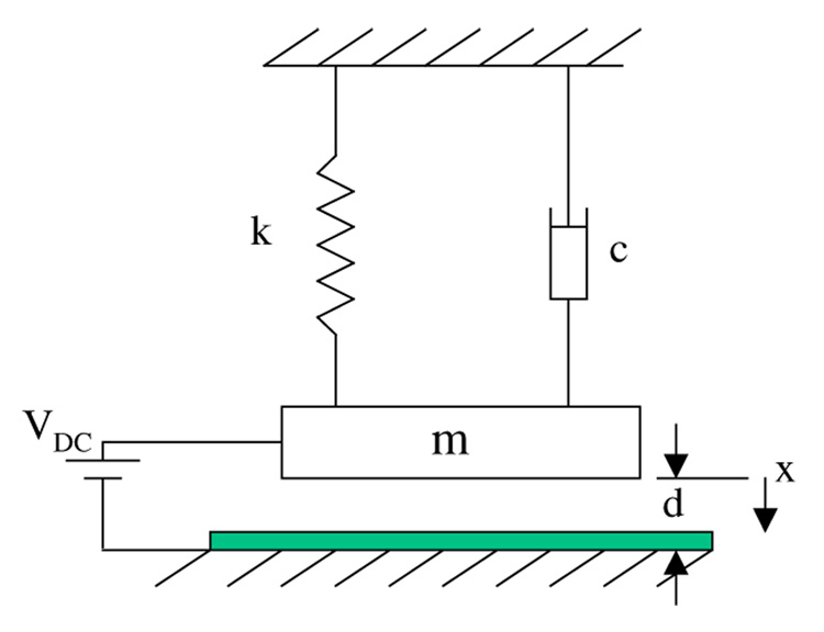
A single-degree-of-freedom model depicted in figure 1 is utilized to represent a MEMS device employing electrostatic actuation and subjected to a shock force Fsh = F0g(t), where F0 is the shock amplitude and g(t) is the shock pulse shape. The device has a movable microstructure of mass m, which forms one side of a variable capacitor. A viscous damper of coefficient c is used to model energy dissipation and a spring of coefficient k is used to model the effective stiffness of the microstructure, which is due to the elastic restoring force and residual stresses. The equation of motion of the microstructure can be written as
| (1) |
,where x is the microstructure deflection, Vdc is the dc polarization voltage, A is the electrode area on the microstructure, d is the capacitor gap width and ε is the dielectric constant of the gap medium. Here, a complete overlapping is assumed between the two electrodes of the capacitor. The shock force is assumed to be a half-sine shock pulse, which is expressed as
| (2) |
where T is the shock duration and u(t) is the unit step function. Equation (1) is integrated with time to determine the response of the microstructure.
Figure 1.
A single-degree-of-freedom model of a MEMS device.
We begin by analyzing the response of a clamped–clamped microbeam employed as a resonant sensor [5], with length L = 510 µm, thickness h = 1.5 µm, width b = 100 µm and gap width d = 1.18 µm. To simplify the analysis, we assume no residual stresses on the microbeam. Using a reduced-order model [27], the pull-in voltage of this microbeam is found to be Vdc ≈ 4.4 V. We use this value in the equation of the pull-in voltage for a simple spring-mass system [25] to extract the stiffness constant k. Another method of determining the stiffness is described in [28] and it leads to a similar result. The details of the development of the reduced-order model for the clamped–clamped beam are given in the following section. We assume a damping ratio ξ = 0.05, which is related to the damping coefficient c as c = 2mω1ξ, where ω1 is the natural frequency of the microstructure.
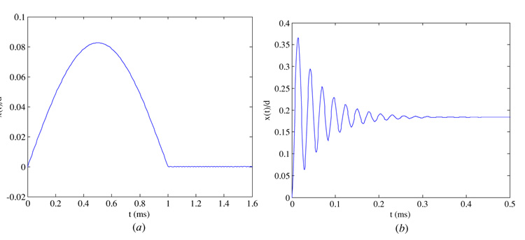
Next, we examine the time response of the microstructure x(t) normalized to the gap width d for various values of the dc voltage and the shock amplitude. In figure 2(a), we set Vdc = 0 and assume a shock amplitude of 1000 g (g refers to the gravitational constant) with duration T = 1.0 ms. As expected, the steady-state value reaches the equilibrium position of zero displacement. Because the natural period of the microstructure is very small (0.02 ms) compared to the duration of the shock load (typically, it ranges from 0.2–1.0 ms for drop table test [29]), we note from figure 2(a) that the microstructure experiences the shock force as a quasi-static force that stays for some time and is then removed. Hence, we note that the response of the microstructure takes a similar shape to the shock pulse profile (quasi-static response). A similar conclusion can be stated for many MEMS devices, as pointed out by Srikar and Senturia [20].
Figure 2.
A time history for the response of a microstructure when actuated by (a) a shock force and no electrostatic force and (b) an electrostatic force and no shock force.
Figure 2(b) shows the time history of the response when Vdc = 4.0 V, and no shock force is applied. We note that the steady-state amplitude is near x(t)/d = 0.175. We recall here that the instability limit of a spring-mass system according to the static analysis is near x(t)/d = 0.33 and according to the dynamic analysis, i.e. accounting for the transients at low damping, is 92% of the static limit, which is x(t)/d = 0.3. This corresponds to a voltage load of Vdc = 4.05 V.
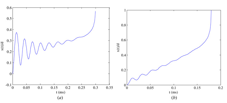
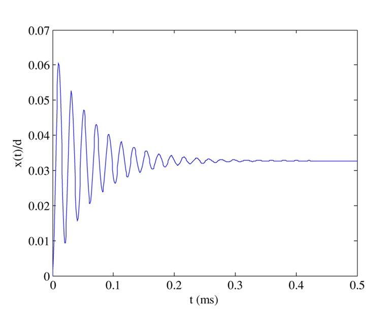
Figure 3(a) shows the time history of the response when Vdc=4.0 V, and a shock load is applied of amplitude 1000 g. It is clear that the system undergoes dynamic pull-in instability, where the electrode hits the substrate. This instability is characterized by the slope of the displacement approaching infinity. Figure 3(b) shows the time history of the response when Vdc = 2.0 V and a shock load is applied of amplitude 10 000 g. Surprisingly, the system also undergoes dynamic pull-in instability, even though the applied voltage of 2.0 V is less than half the static pull-in voltage of 4.4 V or the ‘dynamic’ pull-in voltage of 4.05 V, as explained above. In figure 4, we show the response of the system when Vdc = 2.0 V and no shock force is applied. Clearly, the steady-state response is around x(t)/d = 0.03, which is very far from the pull-in instability limit x(t)/d = 0.3.
Figure 3.
A time history for the response of the microstructure showing dynamic pull-in. In both of these cases, the applied voltage is less than the pull-in voltage of 4.4V, but the response is unstable due to the mechanical shock. (a) Vdc = 4.0 V, shock amplitude = 1000 g and (b) Vdc = 2.0 V, shock amplitude = 10 000 g.
Figure 4.
A time history of the response when Vdc = 2.0 V and no shock force is applied.
Figure 3(b) and Figure 4 indicate very interesting and important results. They show that in the presence of electrostatic forces, a stable system (for example, figure 4), which operates far from the instability threshold, can go unstable under the effect of a shock load that is even moderate in magnitude (in this case, the amplitude ranges from 1000 g–10 000 g). Therefore, in the design of a MEMS device, both the electrostatic forces and the shock forces have to be taken into account, even if the microstructure undergoes small deflection and operates within a small range of the electrostatic force, to avoid this dynamic pull-in instability. This dynamic instability has been reported by Tanner et al [4] as a strange mode of failure, which is characterized by contacts and overlaps among the fingers and electrodes of the parallel-plate capacitors. Figure 5 illustrates the concept of this section.
Figure 5.
Schematic illustrating that the interaction between a shock load and the nonlinear electrostatic force can lead to the early failure of a MEMS device.
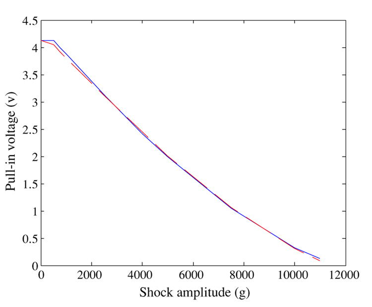
In figure 6, we show a plot of the pull-in voltage of the microstructure against the shock amplitude of a half-sine pulse of duration 1.0 ms (solid) and 0.1 ms (dashed). We note from the figure that the duration of the shock has a slight effect. This is due to the fact that the microstructure does not experience the shock force as shock, as explained before, but rather as a static load. Hence, the structure does not experience any significant difference in the transient response due to those shock loads. As seen from the figure, at a large shock load the microstructure exhibits pull-in instability even if it is biased by a small value of voltage. For example, if the microbeam is biased by a voltage exceeding 1.5 V, it will pull-in at a shock value equal to or greater than 6000 g. It is noted from the figure that at low values of shock, the pull-in voltage of the short-duration shock is lower than that of the higher duration. This can be qualitatively understood by noting figures 2(a) and (b). Figure 2(a) shows that the response to a shock load of T = 1 ms reaches its peak at t = 0.5 ms. On the other hand, we note from figure 2(b) that at t = 0.5 ms, the response of the structure to the electrostatic force alone reaches a steady state and it is almost static (no transient behavior). In the case of the shock load with T = 0.1 ms, the peak of the response occurs at t = 0.05 ms. We can see from figure 2(b) that the deflection at t = 0.05 ms is large, and hence the transient dynamics due to the electrostatic force will be a factor in this case. At higher values of shock loads, the transient effect of the electrostatic force becomes negligible compared to the dominant effect of shock loads.
Figure 6.
A plot of the pull-in voltage of a MEMS microstructure against the shock amplitude of a half-sine pulse of duration 1.0 ms (solid) and 0.1 ms (dashed).
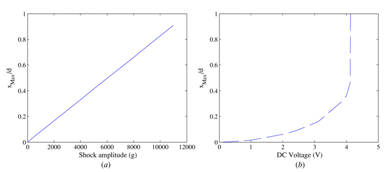
The maximum shock amplitude in figure 6 is equal to 11 000 g. Near such high values of shock, the response of the system due to shock load alone becomes very large and the displacement almost reaches the substrate, as indicated in figure 7(a). The electrostatic force effect becomes very small; however, it is sufficient to cause a contact with the substrate. This is further clarified in figure 7(b), which shows the maximum overshoot value of the displacement due to the actuation of the electrostatic force alone.
Figure 7.
The maximum defection of the microstructure when actuated by (a) a shock force and no electrostatic force and (b) an electrostatic force and no shock force.
To better understand the influence of the simultaneous effect of the mechanical shock and the electrostatic forces on the behavior of electrostatically actuated MEMS devices, we introduce a nondimensional number β that measures the relative strength of the shock force with respect to the electrostatic force at pull-in. This corresponds to x = d/3 for microstructures with linear stiffness. Hence, β can be defined as
| (3) |
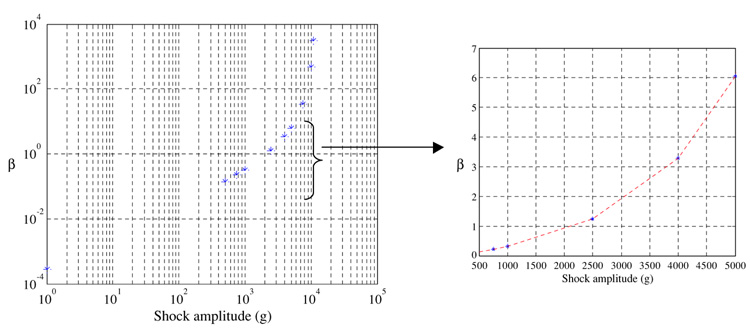
where Vpull is calculated according to the model of equation (1). Figure 8 shows calculated values of β corresponding to the data of figure 6. We note that when β is small and less than one, corresponding to shock values below 2000 g, the shock force is small compared to the electrostatic force. Hence, the shock force has a smaller effect in this regime, and for very small values of β, it has a negligible effect. This is characterized in figure 6 by a nearly flat curve. For this small range of acceleration, it is safe to neglect its effect. However, when β exceeds unity up to 10, which corresponds to shock values from 2000 g to 5000 g, the shock and electrostatic forces become of the same order of magnitude. In this regime, both forces have a considerable influence on the behavior. This regime is characterized in figure 6 by a straight line with almost a constant slope. For larger values of β, the shock force becomes much larger than the electrostatic force. Hence, at these values the shock effect dominates over the electrostatic force effect. For β exceeding one hundreds, it is almost safe to neglect the effect of the electrostatic force on the response.
Figure 8.
Variation of the parameter β for various values of shock amplitude.
3. Beam model
3.1. Problem formulation
The developed SDOF model is helpful to gain qualitative understanding and rough quantitative estimation for the response of a wide range of electrostatically actuated microstructures of regular or irregular shapes. However, for quantitative data and accurate design guidelines, more rigorous models are needed to address the specific details of the microstructure. Reduced-order models can be very efficient to achieve this purpose [27, 30]. In this section, we investigate the behavior of cantilever and clamped–clamped microbeams. These microbeams are widely used in MEMS, such as in microswitches and resonant sensors.
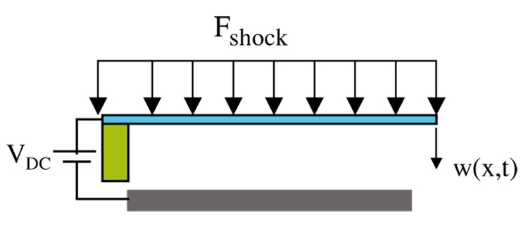
In what follows, a reduced-order model is developed to analyze the response of a microbeam to a shock load and electrostatic force. The derivation is general for microbeams with any boundary conditions. We consider a microbeam, for example, figure 9, actuated by an electrostatic force Vdc and subject to a half-sine shock pulse of amplitude per unit length F0 and shape g(t). The microbeam is subject to a viscous damping, which can be due to squeeze-film damping. We approximate this effect by an equivalent damping coefficient c͂ per unit length. The equation of motion that governs the transverse deflection w(x, t) of the microbeam is written as
| (4) |
where x is the position along the microbeam length, I is the moment of inertia of the cross section, E is Young’s modulus, t is time, ρ is the material density, h and b are the microbeam thickness and width, respectively, d is the gap width and ε is the dielectric constant of the gap medium. The parameter N͂ corresponds to a tensile or compressive axial load, depending on whether it is positive or negative. The integral term in equation (4) represents the mid-plane stretching of the microbeam in the case of immovable boundary conditions. For the case of cantilever microbeams, this term is set to zero.
Figure 9.
An electrostatically actuated microbeam.
For convenience, we introduce the nondimensional variables (denoted by hats)
| (5) |
where t͂ is a time scale, as defined below. Substituting equation (5) into equation (4) and dropping the hats, we obtain
| (6) |
The nondimensional parameters appearing in equation (6) are
| (7) |
The parameter α3 represents a shock amplification factor. According to this parameter, the shock effect increases significantly as the beam length increases and its thickness decreases.
Next, we generate a reduced-order model by discretizing equation (6) into a finite-degree-of-freedom system consisting of ordinary-differential equations in time. The undamped linear mode shapes of the straight (unactuated) microbeam may be used as basis functions in the Galerkin procedure. To this end, we express the deflection as
| (8) |
where ui (t) is the ith generalized coordinate and ϕi (x) is the ith linear undamped mode shape of the straight microbeam. Multiplying equation (6) by ϕi (x) (1 − w)2, substituting equation (8) into the resulting equation and integrating the outcome from x = 0 to 1 yields the reduced-order model. The response of the microbeam to a shock load can be simulated by integrating the ordinary-differential equations of the reduced-order model in time. In a previous study [27], it has been shown that using four or more modes can be sufficient to capture the dynamic response of electrostatically actuated microstructures. Hence, in analyzing the response of a microbeam to mechanical shock and electrostatic force, it is anticipated that the required number of modes should be at least four.
3.2. Response of MEMS devices employing cantilever microbeams
Next, we analyze the dynamic response of MEMS devices employing cantilever microbeams to mechanical shock (figure 10). This problem has been the focus of many recent studies, for example, Coster et al [26], Qian [21] and Tas et al [3]. Cantilever microbeams do not suffer from mid-plane stretching (the integral term in equation (3) is zero). As a case study, we study the response of a silicon cantilever beam with L = 100 µm, h = 0.1 µm, b = 10 µm and d = 2.0 µm. We assume the microbeam to be placed under near-vacuum conditions (no damping), which represents a worst-case scenario. The pull-in voltage of this microbeam based on a static analysis [7, 27] is 0.652 V, and accounting for the transient effect it is 0.6 V.
Figure 10.
An electrostatically actuated cantilever microbeam subjected to mechanical shock.
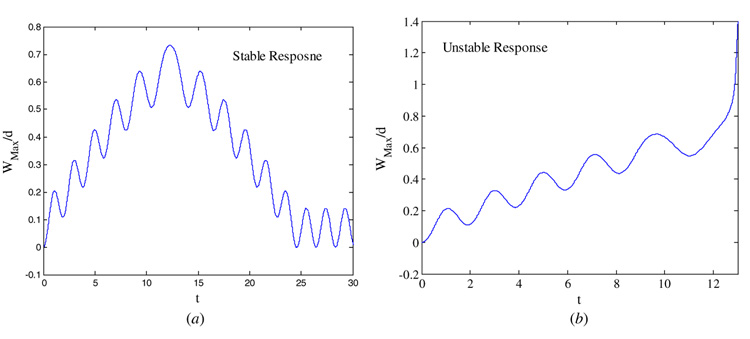
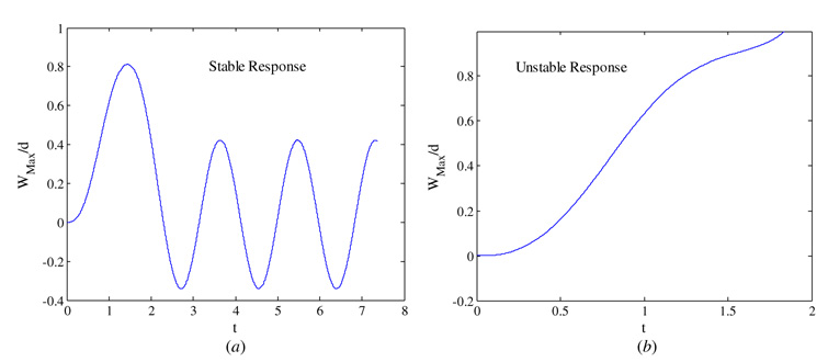
Figure 11(a) shows the time response of the microbeam when actuated by a voltage load Vdc = 0.36 V and subjected to a mechanical shock pulse of amplitude 400 g and duration 1.0 ms. Here, Wmax/d is the maximum deflection of the microbeam at x = L normalized to d, and t is the nondimensional time, as defined in (5). It turns out that the first natural period of the microbeam is much smaller than the pulse duration, and hence the microbeam experiences the mechanical shock as a quasi-static load. We note that the microbeam undergoes large deflection close to the substrate; still the microbeam does not collapse. After the shock, it oscillates around the static equilibrium position due to the effect of the electrostatic force. In other words, the mechanical shock has no permanent effect on the device in this case. In figure 11(b), the dc bias is set to Vdc = 0.37 V. It is clear from the figure that the microbeam undergoes dynamic pull-in and it hits the substrate. This can result in short circuit and stiction problems, and in the case of RF MEMS switches, it can lead to unexpected circuit closing. Figure 12(a) shows the response of the same microbeam when actuated by a voltage load Vdc = 0.27 V and subjected to a 400 g shock pulse of duration 0.1 ms, which is close to the natural period of the microbeam. Hence, the microbeam experiences the shock load as a dynamic load. We also note here that the microbeam undergoes large deflection close to the substrate and does not collapse. However, it oscillates with relatively large amplitude motion after the end of the shock pulse. In figure 12(b), the dc bias is set to Vdc = 0.28 V, in which case the microbeam undergoes dynamic pull-in hitting the substrate.
Figure 11.
The normalized maximum amplitude of a cantilever microbeam subjected to a 400 g shock pulse of T = 1.0 ms versus the nondimensional time. (a) Vdc = 0.36 V, (b) Vdc = 0.37 V.
Figure 12.
The normalized maximum amplitude of a cantilever microbeam subjected to a 400 g shock pulse of T = 0.1 ms versus the nondimensional time. (a) Vdc = 0.27 V, (b) Vdc = 0.28 V.
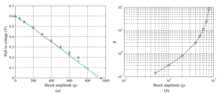
To help validate the above predictions, comparisons are provided in the following with results obtained using the FE software ANSYS [31]. We use the coupled electrostatic-structural element TRANS126 elements to model the electrostatic coupling between the beam and a ground electrode. This element is a two-node element which has one structural degree of freedom and an electrical potential between the nodes. One end of each element is held fixed while the other is coupled to a structural node in the beam. A voltage difference is applied across the TRANS126 element, which creates an attractive force that is resisted by the stiffness of the beam. The shock is applied to all the nodes on the microbeam via the ACEL command using discrete data points during a transient dynamic analysis. Figure 13(a) shows comparisons between the results of the reduced-order model employing four modes (triangles), six modes (stars), seven modes (dash-circles) and the FE model results (solid). We note that as the effect of the electrostatic force decreases for high values of shock load, a larger number of modes is needed to capture the sensitivity in the variation of voltage load. Hence, for low-values of shock loads, using four modes yields acceptable accuracy. For larger values of shock, seven modes yield the most accurate results in agreement with the FE results.
Figure 13.
(a) Cantilever beam response to shock pulse of T = 1.0 ms generated using a dynamic FE model (solid), a reduced-order model employing four (triangles), six (stars) and seven modes (dash-circles). (b) The corresponding β values.
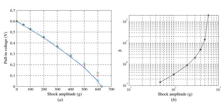
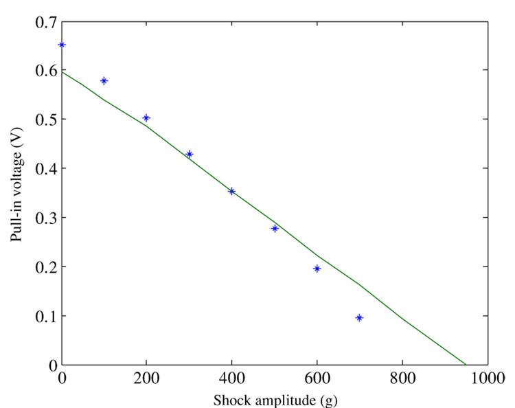
Similar to the SDOF model analysis, we calculate the parameter β to help understand the influence of the simultaneous effect of the mechanical shock and the electrostatic forces on the behavior. Here, the electrostatic force is calculated at Wmax(L) = d/3. Figure 13(b) shows calculated values of β corresponding to the data of figure 13(a). It can be noted that the shock force significantly dominates the electrostatic force for β greater than 10 where the shock amplitude is 600 g. Figure 14 shows similar results for the case of T=0.1 ms. Comparing this figure to figure 13, it is clear that the dynamic amplification of the shock lowers significantly the instability threshold. For example, the microbeam exhibits pull-in for a 600 g shock at a voltage of 0.22 V for a 1.0 ms pulse and at 0.06 V for a 0.1 ms pulse.
Figure 14.
(a) Cantilever beam response to shock of T = 0.1 ms generated using a dynamic FE model (solid), a reduced-order model employing four (triangles), six (stars) and seven modes (dash-circles). (b) The corresponding β values.
It is common in analyzing shock problems in MEMS to model the behavior of microstructures assuming the shock as static forces and solving the mechanical behavior problem as a static problem. This is especially true for microstructures of high natural frequencies that experience the shock force as a quasi-static force. However, for shock–electrostatic problems, this assumption can lead to erroneous predictions since the pull-in instability here is a dynamic instability. This is further explained in figure 15, which shows a comparison between the results of the dynamic model of the electrostatic–shock problem (solid) to those of the static model assuming static electrostatic and shock forces (stars). Both sets of results are obtained using the reduced-order model. It is clear that the static assumption does not yield correct results.
Figure 15.
A comparison between the results of the dynamic model of the electrostatic–shock problem (solid) and those of the static model assuming static electrostatic and shock forces (stars).
3.3. Response of MEMS devices employing clamped–clamped microbeams
Next, we analyze the dynamic response of MEMS devices employing clamped–clamped microbeams to mechanical shock. This problem has been the subject of recent studies, for example, Tas et al, [3], Yee et al [23] and Millet et al [24]. Clamped–clamped microbeams represent an example of microstructures suffering from the geometric nonlinearity mid-plane stretching. As a case study, we study the response of a silicon clamped–clamped beam with L = 900 µm, h = 1.5 µm, b = 100 µm, and d = 2.0 µm. We assume the microbeam to be placed under near-vacuum conditions (no damping), which represents a worst-case scenario. The pull-in voltage of this microbeam based on a static analysis [7, 27] is 3.38 V, and accounting for the transient effect, it is 3.11 V. By calculating the natural frequency of this microbeam, we found that its fundamental natural period is close to 0.1 ms. Hence, the microbeam experiences the mechanical shock load of T=1.0 ms as quasi-static load and of T=0.1 ms as dynamic load.
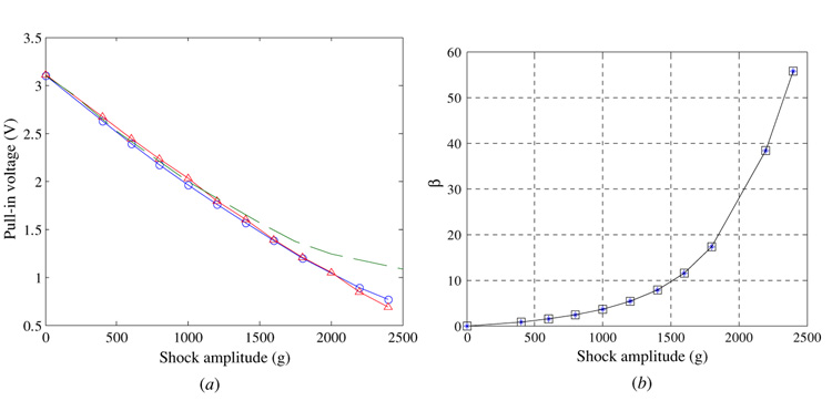
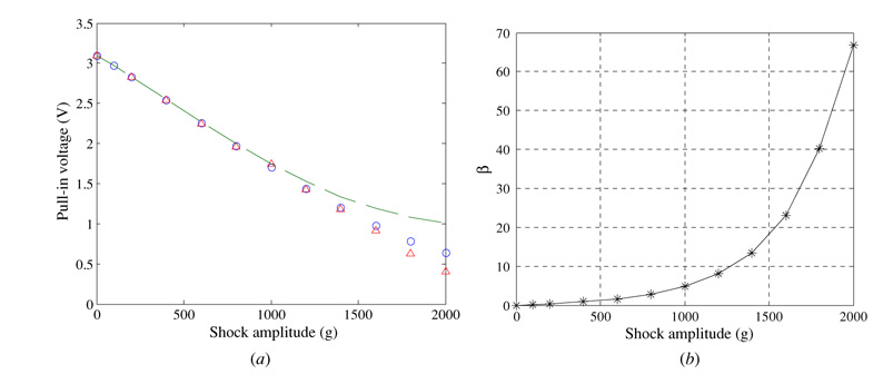
Because of the symmetry of the load and boundary conditions of the microbeam, the symmetric modes are the only modes that participate in the response. Hence, only those are used in the reduced-order model. Figure 16(a) shows comparisons between the results of the reduced-order model employing four modes (dashed), six modes (solid-circle) and the FE model results (solid-triangle). It is clear that using six modes are sufficient to capture the dynamic behavior. It should be mentioned that we were unable to use more than six symmetric modes in our Mathmatica code [32] because of convergence problems in the numerical integration of the higher order mode shapes. Also, beyond a shock value of 2400 g, it is difficult to distinguish a sharp and sudden transition in the response as a sign of dynamic pull-in in both the FE model and the reduced-order model. This is because, as indicated from figure 16(b), the shock force becomes significantly dominant over the electrostatic force. Figure 17 shows similar results for the case of T = 0.1 ms.
Figure 16.
(a) Clamped–clamped beam response to shock of T = 1.0 ms generated using a dynamic FE model (solid-triangle), a reduced-order model employing four (dashed) and six (solid-circles) modes. (b) The corresponding β values.
Figure 17.
(a) Clamped–clamped beam response to shock of T = 0.1 ms generated using a dynamic FE model (triangle), a reduced-order model employing four (dashed) and six (circles) modes. (b) The corresponding β values.
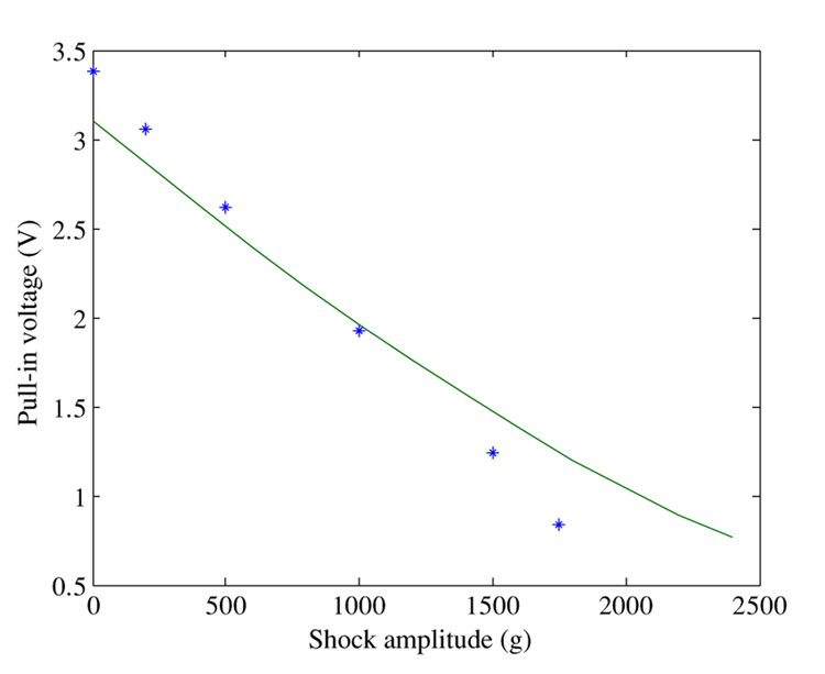
With regard to treating the shock–electrostatic problem as a static problem assuming static forces, the conclusion of the case of cantilever microbeams is still held for clamped–clamped microbeams. This is illustrated in figure 18, which shows a comparison between the results of the dynamic model of the electrostatic–shock problem (solid) to those of the static model assuming static electrostatic and shock forces (stars). Clearly, the static assumption is not adequate to capture accurately the pull-in instability location.
Figure 18.
A comparison between the results of the dynamic model of the electrostatic–shock problem (solid) and those of the static model assuming static electrostatic and shock forces (stars).
4. A smart MEMS switch triggered by acceleration
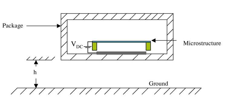
A primary aim of the present work is to help mitigate the adverse effects of combined shock and electrostatic forces. However, one can also take advantage of these combined effects in the development of newdevices. One example of this is a smart MEMS switch, which is triggered by acceleration. The device, shown in figure 19, consists of an active switch where the applied dc voltage is used to set the acceleration level where instability occurs. One could tune the dc voltage on the microbeam so that it collapses when the device experiences acceleration beyond a specific threshold. Below the threshold, the beam deflects only slightly due to acceleration. If the acceleration exceeds a specific threshold, themicrobeam snaps down to close an electric circuit as a switch. This switching mechanism is very desirable in many applications, such as to trigger airbags in vehicles and to protect portable devices upon impact [33].
Figure 19.
Schematic for a packaged MEMS switch being dropped from height h to the ground. Such an impact induces shock force on the package, which is transferred to the microstructure in the form of an acceleration pulse.
The principle of operation of the new switch can be further illustrated by considering any of figure 6, Figure 13(a), Figure 14(a), Figure 16(a) and Figure 17(a). For any point of acceleration and voltage to the right of a shock-voltage curve, the switch is on; otherwise, the switch is off. For example, in figure 13(a), if the microbeam is biased by 0.2 V and is subjected to an acceleration of 600 g, it will collapse and the switch will be on. The switch can be tuned to operate at any desired acceleration level (ranging from zero to hundreds of thousands of g’s) by modifying its design parameters, such as the structure shape and its dimensions.
Figure 6, Figure 13(a), Figure 14(a), Figure 16(a) and Figure 17(a) demonstrate tunable switches with operation ranges of hundreds to thousands of g’s. Some applications however require that the switch be triggered at a lower acceleration range. In these applications, the switch and its package may not be subjected to shock force, which induces large values of acceleration. For example, to protect portable devices, such as a laptop computer, when falling the switch has to function once it feels free falling, which induces acceleration, equal to 1 g. If the laptop hits the ground, it is too late to protect the hard drive. So it is desired that the switch be triggered at a level of unity g before the impact to protect the hard drive during the impact.
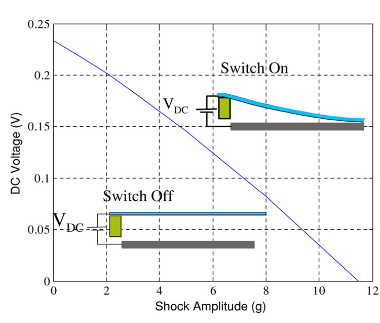
To lower the operation range of the switch, the geometry of the cantilever microbeam of figure 13 can be modified. We choose the microbeam to have L = 900 µm, h = 1.0 µm, b = 100 µm and d = 2.0 µm. Figure 20 depicts the dc voltage threshold versus the shock amplitude for a half-sine shock pulse of duration equal to 1.0 ms. For any point of shock amplitude and voltage to the right of the curve, the microbeam hits the substrate and the switch is on; otherwise, the microbeam does not collapse and the switch is off. We note here that the operation range of the switch has been lowered significantly to a maximum of 12 g. This means that the switch is more sensitive to variation in acceleration in this low range.
Figure 20.
A plot of the actuation threshold of the smart switch against the shock amplitude of a half-sine pulse of duration 1.0 ms. For any point of shock amplitude and voltage to the right of the curve, the switch is on; otherwise, the switch is off.
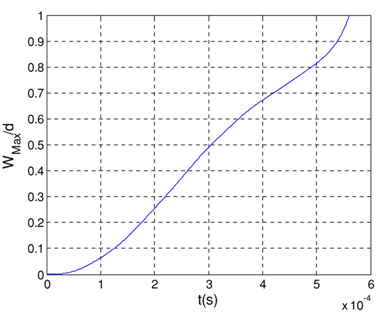
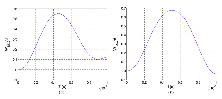
Next, we demonstrate the sensitivity of this switch to variation in the dc voltage and the acceleration level. As an example, we suppose that the desired threshold for the switch closing is at an acceleration level equal to 4 g or larger. According to figure 20, we need to apply a dc voltage of 0.17 V on the microbeam to have a pull-in at 4 g. Figure 21 shows the time response of the microbeam when biased by 0.17 V and subjected to a shock pulse of amplitude 4 g. It is clear that the microbeam hits the substrate (close the switch) when Wmax/d = 1. Figure 22(a) shows a similar plot, but by adjusting the voltage to 0.16 V. It is clear that the switch does not close in this case (remains in the off position). Figure 22(b) shows a plot similar to figure 21, but here the level of acceleration has been lowered to 3 g. We can also note here that the switch does not close and remains in the off position. We conclude from figure 21 and Figure 22 that this switch can be tuned to close accurately at the desired acceleration level. Below the desired threshold of acceleration, the switch does not close (figure 22(a)). Also, lowering the voltage bias below the required threshold makes the switch not closing (figure 22(b)).
Figure 21.
The time response of the cantilever microbeam to a half-sine shock pulse of amplitude 4 g and dc voltage 0.17 V showing the switch in the on state.
Figure 22.
The time response of the cantilever microbeam showing the switch in the off state. (a) Pulse amplitude is 3 g and dc voltage 0.17 V, (b) pulse amplitude is 4 g and dc voltage 0.16 V.
5. Summary and conclusions
We presented modeling and simulation of MEMS devices under the combination of shock loads and electrostatic actuation. Our results indicate that the reported strange failures of electrostatically actuated microstructures under shock load can be attributed to early dynamic pull-in instability. The results show that the combination of a shock load and an electrostatic actuation makes the instability threshold much lower than the threshold predicted considering the effect of shock alone or electrostatic actuation alone.
We utilized a single-degree-of-freedom model to investigate the effect of the shock–electrostatic interaction on response of MEMS devices with microstructures of general shapes. We then used a reduced-order model to demonstrate the effect of this interaction on MEMS devices employing cantilever and clamped–clamped microbeams and verified the results by comparing to finite-element predictions. We showed that the shock–electrostatic interaction could be used to design smart MEMS switches triggered at a predetermined level of shock and acceleration. We investigated the potential application of this switch for low-g and high-g applications and demonstrated its sensitivity for variations in acceleration and dc voltage.
It is concluded that three zones characterizing shock–electrostatic problems can be distinguished based on the magnitude of the shock pulse compared to the electrostatic force at pull-in (the parameter β). The first zone is for very small values of β, approximately less than 0.2. In this regime, the shock force has a negligible or minor effect on pull-in. The second zone is for large values of β exceeding 50. In this regime, the electrostatic force has a minor to negligible effect on the deflection of the microstructure. The third zone lies between the previous two. It is the largest and the most dangerous zone since both the electrostatic and mechanical shock forces have considerable effect on the response. In this region, it is unsafe to neglect the effect of either force.
It has been demonstrated that modeling the electrostatic–shock interaction problem as a static problem by approximating the shock force as a quasi-static force can lead to erroneous results. It is observed that the computational cost of simulation increases with increasing values of β. This is manifested through the requirement of larger number of modes or basis functions to be used in the reduced-order model and finer mesh and more elements in the finite-element models. This is attributed to the fact that it becomes difficult to capture the sensitivity of the response to changing the dc voltage for shock-dominated regimes.
Footnotes
(Some figures in this article are in colour only in the electronic version)
References
- 1.Brown TG. Harsh military environments and microelectromechanical (MEMS) devices; Proc. IEEE Sensors; 2003. pp. 753–760. [Google Scholar]
- 2.Wagner U, Franz J, Schweiker M, Bernhard W, Muller-Fiedler R, Michel B, Paul O. Mechanical reliability of MEMS-structures under shock load. Microelectron. Reliab. 2001;41:1657–1662. [Google Scholar]
- 3.Tas N, Sonnenberg T, Jansen H, Legtenberg R, Elwenspoek M. Stiction in surface micromachining. J. Micromech. Microeng. 1996;6:385–397. [Google Scholar]
- 4.Tanner DM, Walraven JA, Helgesen K, Irwin LW, Smith NF, Masters N. Int. Reliability Physics Symp. San Jose, CA, 2000: 2000. MEMS reliability in shock environments; pp. 129–138. [Google Scholar]
- 5.Tilmans HA, Legtenberg R. Electrostatically driven vacuum-encapsulated polysilicon resonators: II. Theory and performance. Sensors Actuators A. 1994;45:67–84. [Google Scholar]
- 6.Osterberg PM, Senturia SD. M-TEST: a test chip for MEMS material property measurement using electrostatically actuated test structures. J. Microelectromech. Syst. 1997;6:107–118. [Google Scholar]
- 7.Abdel-Rahman EM, Younis MI, Nayfeh AH. Characterization of the mechanical behavior of an electrically actuated microbeam. J. Micromech. Microeng. 2002;12:795–766. [Google Scholar]
- 8.Ananthasuresh GK, Gupta RK, Senturia SD. An approach to macromodeling of MEMS for nonlinear dynamic simulation; Proc. ASME Int. Conf. of Mechanical Engineering Congress and Exposition (MEMS) (Atlanta, GA, 1996); 1996. pp. 401–407. [Google Scholar]
- 9.Krylov S, Maimon R. Pull-in dynamics of an elastic beam actuated by distributed electrostatic force; Proc. 19th Biennial Conf. in Mechanical Vibration and Noise (VIB), (Chicago, IL, 2003); 2003. DETC2003/VIB-48518. [Google Scholar]
- 10.Nayfeh AH, Younis MI, Abdel-Rahman EM. Dynamic analysis of MEMS resonators under primary resonance excitation; Proc. 20th Biennial Conf. on Mechanical Vibration and Noise (VIB) (Long Beach, CA, 2005); 2005. DETC2005-84146. [Google Scholar]
- 11.Béliveau A, Spencer GT, Thomas KA, Roberson SL. Evaluation of MEMS capacitive accelerometers. Des. Test Comput. 1999;16:48–56. [Google Scholar]
- 12.Brown TG, Davis BS. Dynamic high-g loading of MEMS sensors: ground and flight testing; Proc. SPIE-Int. Soc. Opt. Eng; 1998. pp. 228–235. [Google Scholar]
- 13.Brown TG, Davis B, Hepner D, Faust J, Myers C, Muller P, Harkins T, Hollis M, Miller C, Placzankis B. Strap-down microelectromechanical (MEMS) sensors for high-g munition applications. IEEE Trans. Magn. 2001;37:336–342. [Google Scholar]
- 14.Li GX, Shemansky JR. Drop test and analysis on micro-machined structures. Sensors Actuators A. 2000;85:280–286. [Google Scholar]
- 15.Cunningham S, McIntyre D, Carper J, Jaramillo P, Tang WC. Microstructures designed for shock robustness; Proc. SPIE—Int. Soc. Opt. Eng; 1996. pp. 99–107. [Google Scholar]
- 16.Lim BB, Yang JP, Chen SX, Mou JQ, Lu Y. Shock analysis of MEMS actuator integrated with HGA for operational and non-operational HDD; Dig. of the Asia-Pacific Magnetic Recording Conf; 2002. pp. WE-P-18-01–WE-P-18-02. [Google Scholar]
- 17.Atwell AR, et al. Simulation, fabrication and testing of bulk micromachined 6H-SiC high-g piezoresistive accelerometers. Sensors Actuators. 2003;104:11–18. [Google Scholar]
- 18.Jiang Y, Du M, Huang W, Xu W, Luo L. Simulation on the encapsulation effect of the high-g shock MEMS accelerometer; Proc. 5th Int. Conf. on Electronics Packaging Technology (Shanghai, 2003); 2003. pp. 52–55. [Google Scholar]
- 19.Fan MS, Shaw HC. Dynamic response assessment for the MEMS accelerometer under severe shock loads. National Aeronautics and Space Administration, NASA (Goddard Space Flight Center, Greenbelt, MD) 2001 TP—2001–209978. [Google Scholar]
- 20.Srikar VT, Senturia SD. The reliability of microelectromechanical systems (MEMS) in shock environments. J. Microelectromech. Syst. 2002;11:206–214. [Google Scholar]
- 21.Qian Z, Tomase J, Lian K. Mechanical simulation for the robust design of RF-MEMS switches; Proc. ASME Int. Conf. of Mechanical Engineering Congress and Exposition (MEMS) (Anaheim, CA, 2004); 2004. p. 60112. [Google Scholar]
- 22.Fang XW, Huang QA, Tang JY. Modeling of MEMS reliability in shock environments; Proc. 7th Int. Conf. on Solid-State and Integrated Circuits Tech., Beijing; 2004. pp. 860–863. [Google Scholar]
- 23.Yee JK, Yang HH, Judy JW. Shock resistance of ferromagnetic micromechanical magnetometers. Sensors Actuators A. 2003;103:242–252. [Google Scholar]
- 24.Millet O, Collard D, Buchaillot L. Reliability of packaged MEMS in shock environments: crack and stiction modeling; Proc. Design, Test, Integration and Packaging of MEMS/MOEMS (Cannes); 2002. pp. 696–703. [Google Scholar]
- 25.Senturia SD. Microsystem Design. Boston: Kluwer; 2000. [Google Scholar]
- 26.Coster JD, Tilmans HC, van Beek JTM, Rijks TGSM, Puers R. The influence of mechanical shock on the operation of electrostatically driven RF-MEMS switches. J. Micromech. Microeng. 2004;14:S49–S54. [Google Scholar]
- 27.Younis MI, Abdel-Rahman EM, Nayfeh AH. A reduced-order model for electrically actuated microbeam-based MEMS. J. Microelectromech. Syst. 2003;12:672–680. [Google Scholar]
- 28.Pamidighantam S, Puers R, Baert K, Tilmans HAC. Pull-in voltage analysis of electrostatically actuated beam structures with fixed-fixed and fixed-free end conditions. J. Micromech. Microeng. 2002;12:458–464. [Google Scholar]
- 29.Solid State Technology Association. Arlington, VA: 2003. JEDEC Board Level Drop Test Method of Components for Handheld Electronic Products Standard No. JESD22-B111. [Google Scholar]
- 30.Nayfeh AH, Younis MI, Abdel-Rahman EM. Reduced-order models for MEMS applications. Nonlinear Dyn. 2005;41:211–236. [Google Scholar]
- 31.ANSYS, Inc. Version 10. Canonsburg, PA: 2005. www.ANSYS.com. [Google Scholar]
- 32.Wolfram Research, Inc. Mathematica, Version 5.2. Chapaign, IL: 2005. 2005 http://www.wolfram.com/products/mathematica/index.html. [Google Scholar]
- 33.Man PF, Mastrangelo CH. Surface micromachined shock sensor for impact detection. Solid-State Sensor and Actuato Workshop (Hilton Head) 1994:156–159. [Google Scholar]


