Abstract
Carbon electrodes coupled with electrochemical detection have been used extensively for the investigation of biogenic amines. Herein we report the fabrication and characterization of carbonaceous electrodes prepared from pyrolyzed parylene C (PPC) films. High-aspect ratio carbonaceous microelectrodes have been prepared by masking PPC coated pipettes with an insulating parylene C film. PPC thin film electrodes were characterized electrochemically, spectroscopically, and with electron microscopy. The procedures described here offer a route to fabrication of thin film carbon electrodes that can be patterned and produced in parallel. These electrodes are similar to carbon electrodes derived from pyrolyzed photoresist films but do not require spin-coating or lithography and can readily coat three-dimensional surfaces.
INTRODUCTION
A variety of methods exist for the preparation of micro and nanoscale electrodes.1,2,3,4,5,6,7,8 Here, we describe the construction of carbon microelectrodes through the use of thermally pyrolyzed parylene C (PPC). Electrodes are characterized electrochemically, spectroscopically and with electron microscopy. Microelectrodes are prepared by subjecting a parylene C-coated pipette to pyrolysis. An additional layer of insulating parylene is subsequently deposited to render a microelectrode.
Encapsulated fibers and microfabricated structures are two of the most common methods utilized to form small-scale electrodes. Carbon microelectrodes find special utility for the measurement of biological species such as neurotransmitters.1,9,10,11 Typically, to form small carbon electrodes, carbon fibers are etched and encapsulated in an insulating material such as glass or an electropolymerized layer.3,8,12 In addition to this method, a number of alternative routes to prepare carbon electrodes have been developed. For instance, carbon coated pipettes have been prepared through chemical vapor deposition.13,14,15 An alternative route to form carbon electrodes is found in pyrolyzed photoresist films (PPFs).16,17,18 When pyrolyzed in a reducing atmosphere, removal of heteroatoms from the photoresist structure and subsequent reduction of the film results in formation of a conducting carbon film. Advantages of PPFs include the ability to pattern electrodes with high spatial resolution.19,20,21 Previous reports have demonstrated that PPF-coated tungsten wires possess properties suitable for electrochemical measurement.21,22
Parylene coatings possess high electrical and chemical resistance and find utility in microelectronic 23,24,25 and biomedical applications.26,27 As described in previous reports, pyrolysis under an inert atmosphere converts the highly insulating parylene layer to a conductive carbon film, which provides an alternate to formation of carbon electrodes from thin films.17,28 Parylene deposition and polymerization is a low-temperature process that can produce thin (tens of nanometers) conformal coatings with low defect densities. The ability to coat three-dimensional or high aspect ratio structures without the need for spin-coating or complicated manipulations is particularly attractive.
Here we detail deposition of parylene C, pyrolysis to form a conductive film and insulation with additional parylene layers for the formation of carbon electrodes. The process described provides a simple fabrication method for carbonaceous thin film electrodes or microelectrodes supported on a pipette. Chemical transformation of pyrolysis is confirmed both by the Raman spectra of pyrolyzed thin films and by thermal gravimetric analysis (TGA). Electrochemical evaluation is performed for thin film electrodes. Pipettes are masked to form three-dimensional electrodes, which subsequently are characterized by electrochemical methods and electron microscopies. The procedures described here offer a route to fabrication of thin film carbon electrodes that can be patterned and produced in parallel. These electrodes are similar to carbon electrodes derived from pyrolyzed photoresist films but do not require spin-coating or lithography and can readily coat three-dimensional surfaces.
EXPERIMENTAL
Materials
Hexaammineruthenium (III) chloride (99 %) (Strem Chemicals, Newburyport, MA) and dopamine hydrochloride (Sigma-Aldrich, St. Louis, MO) were used for electrochemical characterization of fabricated microelectrodes and films. Potassium chloride or phosphate buffered saline served as electrolyte. Dichloro-[2,2]-paracyclophane (parylene C dimer) was used as received (SCS Coatings, Indianapolis, IN). Poly(dimethylsiloxane) (PDMS) (Sylgard 184, Dow Corning, Midland, MI) was used to mask the tips of pipettes in the microelectrode fabrication process.
Preparation of Pyrolyzed Parylene C (PPC)
Chemical vapor deposition (CVD) of parylene C on silicon or quartz materials was performed with a commercial parylene deposition system (Labcoter 2/PDS 2010, SCS Coatings). Vaporizer and pyrolysis heater setpoints were 175° C and 690° C, respectively. Parylene films were pyrolyzed in a furnace (Lindberg, Riverside, MI) at 900 °C for one hour under an inert N2 atmosphere.
Microelectrode Fabrication
Quartz pipettes were fabricated from 1.0 mm outer diameter, 0.68 mm inner diameter quartz capillaries with a P-2000 laser puller (Sutter Instruments, Novato, CA). To pull pipettes with an inner diameter of ~150 nm, parameters of Heat= 670, Filament= 3, Velocity= 41, Delay= 180, Pull= 165 were used. Pipettes were mounted in the parylene deposition chamber, such that the large end of the pipette was closed with carbon tape. Chemical vapor deposition of parylene C was then performed with the settings described above. Pyrolysis was performed at 900°C for one hour to render a carbonaceous film which coated the entire exposed area of the pipettes. Insulation of the conductive pipette was performed through two consecutive depositions of parylene C to ensure sealing of possible pinhole leaks. During this insulation step, pipettes were stood on end with the tip of the pipette inserted into a thin layer of PDMS. This procedure allowed for the entire pipette to be insulated except for an exposed area at the tip, which served to form the electrode.
Film and Microelectrode Characterization
Both scanning electron microscopy (SEM) and cyclic voltammetry were utilized to characterize carbon films on silicon wafers (0.25 cm2 exposed electrode area) and quartz pipettes. Cyclic voltammetry was obtained in both 5 mM Ru(NH3)63+, with 0.1 M KCl as the supporting electrolyte, and 100 μM dopamine hydrochloride, with 0.1 M phosphate buffered saline buffer (pH = 7.4) as the supporting electrolyte. A Pt wire and a Ag/AgCl wire served as the auxiliary and reference electrodes respectively in a three-electrode cell. A Quanta-FEG FE-SEM (FEI, Hillsboro, OR) was used for characterization. A JEOL JEM 3200FS transmission electron microscope (TEM) (JEOL USA, Inc., Peabody, MA) was also used for characterization, with images collected at 300kV accelerating voltage. A Q5000 thermogravimetric (TGA) instrument (TA Instruments, New Castle, DE) was used to calculate percent weight loss of PPC. Raman measurements were performed with a Renishaw inVia Raman microscope (Renishaw, Gloucestershire, United Kingdom) fitted with a diode laser for excitation at 785 nm. A light microscope (Leica microsystems, Bannockburn, WI) with a 50x long-working distance objective (numerical aperture 0.5) or a 50x short-working distance objective (numerical aperture of 0.75) was interfaced with the Raman instrument. UV-Vis measurements were recorded with an Agilent 8453 UV-Visible spectrophotometer (Santa Clara, CA).
RESULTS AND DISCUSSION
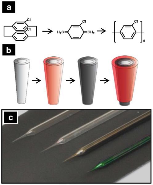
The chemical process for the formation of parylene C films is shown in Figure 1a. Dichloro-[2,2]-paracyclophane is vaporized and then thermally pyrolyzed (temperature ca. 600 °C) to form a reactive monomer species. Pyrolyzed monomers deposit on materials within the deposition chamber and undergo free radical polymerization to form a poly(parylene) thin film. The pyrolyzed film is highly insulating, possesses a low defect density and exhibits exceptional chemical stability. Control over film thickness is achieved through the mass of monomer initially vaporized. Poly(parylene) deposits onto virtually any surface, regardless of surface roughness, aspect ratio or conductivity.
Figure 1.
(a) Parylene reaction scheme. (b) A schematic of the microelectrode fabrication process from a bare pipette to a final pyrolyzed microelectrode. A bare quartz pipette (far left) is coated with a thin layer of parylene C and subsequently pyrolyzed under an inert atmosphere. The pipette is then masked and insulated with another layer of parylene C to form a carbon electrode (far right). (c) Optical micrographs of pipettes at different stages of this process. From left to right: a bare pipette, a pipette after initial parylene C deposition, after pyrolysis of parylene C and a final parylene-insulated carbonaceous pipette.
In Figure 1b, the process to form microelectrodes is depicted. First, a quartz pipette is formed. Next, a conformal parylene C film is deposited onto the quartz pipette. Pyrolysis of the poly(parylene) coating at 900 °C under a N2 atmosphere results in a conductive thin film on the exterior of the pipette. Due to the lower melting or softening point of borosilicate glass, the use of quartz or silicon under these circumstances is critical. Pipettes are then stood on-end in a thin film of PDMS with the tip of pipette down. As mounted, pipette tips penetrate into the PDMS film, which serves to mask the tip of the pipette upon subsequent exposure to a second film of parylene to insulate the body of the pipette. An optical micrograph of pipettes at each stage of this process is shown in Figure 1c. Pipettes from top to bottom represent each stage of fabrication shown in Figure 1b. After pyrolysis, a metallic sheen is observable on the surface of the pipette (Figure 1c, third from top). This film, when examined with electron microscopy, is uniform and defect-free. Subsequent insulation results in a visible change in color of the pipette body (Figure 1c, bottom pipette).
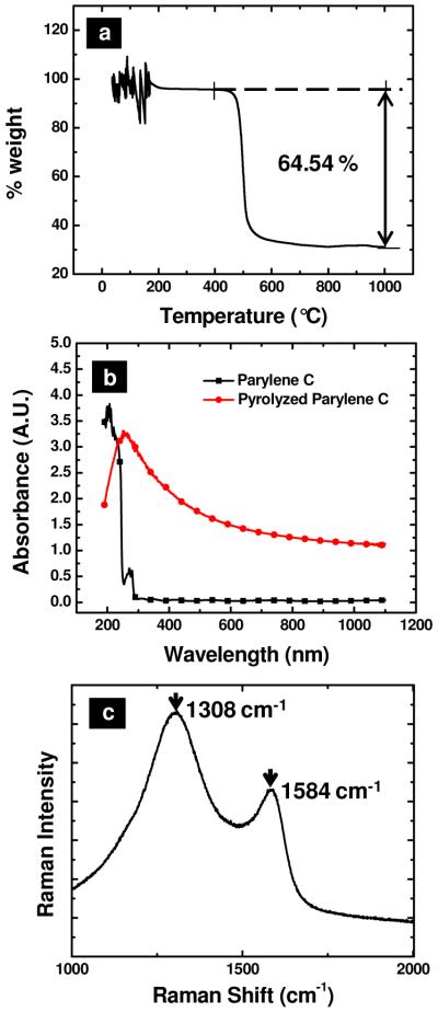
Thin films on silicon wafers or quartz slides were characterized via TGA and spectroscopy, as demonstrated in Figure 2, and are in good agreement with previous reports.29,30 In Figure 2a, TGA of poly(parylene) heated under an inert atmosphere over a range from 0 to 1000 °C is shown. A single, abrupt event at ca. 500 °C corresponds to 65% mass loss. Spectroscopic characterization of poly(parylene) by UV-vis absorbance and Raman spectroscopies are shown in Figure 2(b-c). Prior to pyrolysis (Figure 2b), poly(parylene) films demonstrated significant absorbance below 300 nm but were transparent at greater wavelengths. After pyrolysis, PPC films exhibited broad absorbance over the spectral range measured. Visually, as described above, films were observed to have a metallic sheen post pyrolysis, suggesting that scattering/reflection contribute significantly to the response observed. Raman spectra could not be baseline resolved and are similar to previous reports for PPF films that demonstrate a carbon structure with both disordered and graphitic character.29 Post pyrolysis (Figure 2c), the Raman spectra possessed two broad peaks at ca. 1308 cm−1 and 1584 cm−1, indicative of the “D” (disorder) and “G” (graphitic) bands respectively.29 These assignments agree well with previous measurements that detail sp2 hybridized carbon, in which the G band lies at a wavelength characteristic for graphitized carbon.29,31 While the origins of the D band have been debated, the Raman shift observed has been shown to be dependent on excitation wavelength. In spectra recorded here, an excitation wavelength of 785 nm was used and resulted in good agreement to previous reports for D bands measured for graphitic materials excited at 782 nm.32 Gaussian peak fits of integrated peak intensity determined a relatively high D/G ratio (~3-4), indicating the film possesses substantial disorder. In experiments reported here, pyrolysis has been performed under N2 as opposed to a more reductive environment of forming gas. This possibly results in the lower film order and higher resistances (vide supra) observed. However, it is of note that conductive films were obtained without the introduction of H2, as the chemical structure of parylene C does not possess nitrogen atoms and has a low initial concentration of heteroatoms (only Cl) in contrast to typical photoresists used for PPF electrode preparation.
Figure 2.
(a) Thermogravimetric analysis of parylene c in a nitrogen atmosphere. (b) UV-visible absorbance of 1.0 g of parylene c (-■-) and pyrolyzed parylene c ( ) deposited on a quartz substrate. (c) Averaged Raman spectra (n = 10) of amorphous pyrolyzed parylene. Characteristic G and D modes are visible at 1308 cm−1 and 1583 cm−1 respectively in (d). λexc = 785 nm, 10 mW power average.
PPC films were also coated onto grids for TEM and onto pulled quartz pipettes. A transmission electron micrograph of a PPC film is shown in Figure 3a. Here, well-ordered carbon exhibiting lattice fringes is observed. Crossed lattice fringes, which are formed by the intersection of two or more lattice fringes, are also present. Ordered domains were observed inconsistently when sampled over large areas of the film, as some areas possessed a higher content of amorphous carbon. Images subjected to FFT displayed peaks indicating small atomic spacing. The smallest spacing that was calculated was 1.12 Å, based on the distance between the central spot and the outermost spot. The spacing between the center spot and the outer two rings indicate ordered sp2 carbon spacing of approximately 2.49 Å and 4.189 Å, respectively. Figure 3c shows a scanning electron micrograph of a microelectrode prepared as described in Figure 1. A conical region at the tip of pipette is observed. Electrodes that were not allowed to contact the PDMS masking layer during preparation exhibited no detectable electrochemical response, which demonstrates that the two-step process for parylene deposition employed here produces a defect-free insulating layer. The pipette in this image has two regions clearly identifiable. The tip region of the pipette over the first ~100 microns is composed of PPC. A region comprised of unpyrolyzed parylene C further up the shank of the pipette can also be identified. For this particular pipette, the opening was closed by the PPC coating. It was possible, however, to prepare open pipettes as well as ring-type pipettes using similar deposition and insulation protocols. Overall the method described is sufficient to prepare PPC electrodes with isolated regions at the end of a pipette. Overall, a success rate of ~47% for the batch fabrication (n>20 per batch) of PPC microelectrodes with tip diameters ≤2 μm was achieved. Further control over the geometries and dimensions of electrodes prepared is desirable and is being investigated further.
Figure 3.
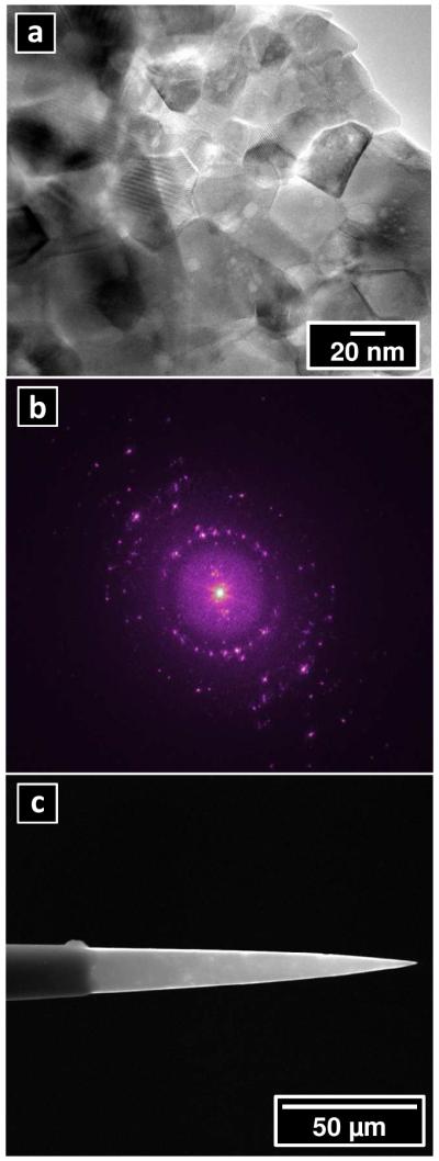
(a) Transmission electron micrograph of pyrolyzed parylene C thin film. (b) FFT of electron micrograph showing diffraction and film order. (c) Scanning electron micrograph of pyrolyzed parylene C electrode as prepared.
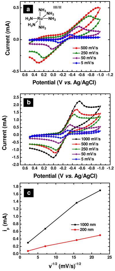
Electrochemical characterization of PPC thin films with the model outer-sphere redox probe Ru(NH3)63+/2+ is shown in Figure 4. Here, the effect of film thickness was evaluated for PPC films with thicknesses of approximately 200 and 1000 nm (Figure 4a and b, respectively). The dependence of peak current on the square root of scan rate yielded a linear relationship, indicating semi-infinite linear diffusion. The relationship for peak current(uncorrected) with scan rate is plotted in Figure 4c. For PPF electrodes, electrochemical responses with significant contributions related to the sheet resistance of the thin carbon film have been reported.33 Both PPC film thicknesses show relatively linear response with scan rate. However, more pronounced peak splitting is observed in the case of 200 nm films, which suggests an increase in sheet resistance for thinner films. Voltammetry recorded at 200 mV/s exhibited uncorrected ΔEps of 950 mV and 480 mV for the 200 nm and 1000 nm thick films respectively. For the 1000 nm thick film, the uncorrected ΔEp for the PPC film is 4-5 times higher than that reported for a PPF film of similar thickness. Raman spectra recorded showed significantly higher D/G ratios for PPC films relative to PPF films, indicating the overall graphitic content of the PPC film is significantly lower than PPF. The greater ΔEp observed is in agreement with this result and suggests that the increased sheet resistance leads to greater uncompensated resistance in electrochemical measurements for PPC films.
Figure 4.
Voltammetric response in 5 mM Ru(NH3)63+, with 0.1 M KCl as a supporting electrolyte, of 200 nm (a) and 1000 nm (b) thick films of pyrolyzed parylene C on a silicon surface (A = 0.25 cm2), at varying scan rates. Ag/AgCl reference and Pt counter electrodes were utilized for all cyclic voltammetry measurements. (c) Plot of uncorrected peak current as a function of scan rate for 200 nm and 1000 nm pyrolyzed parylene C films.
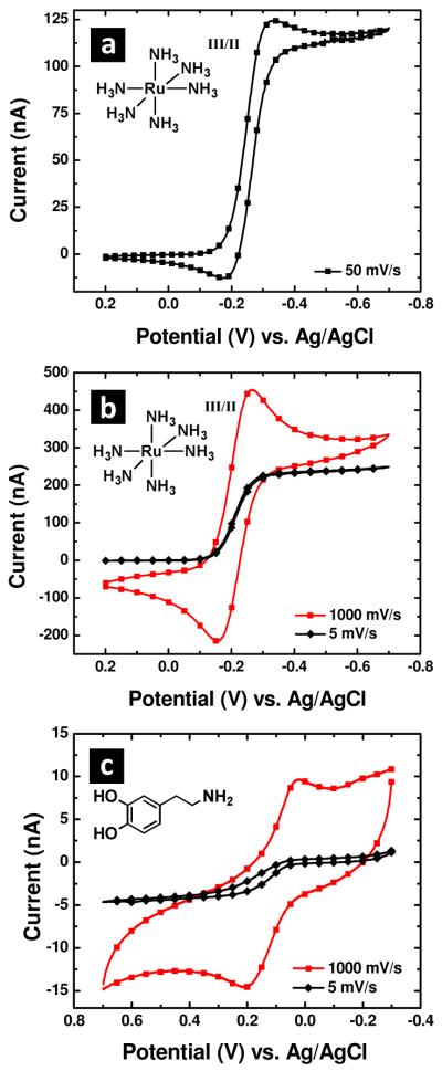
Electrochemical evaluation of PPC coated and poly(parylene) insulated pipettes was also examined. The electrochemical response of the electrode shown in Figure 3c displayed a quasi-steady state response in ruthenium hexamine (Figure 5a). From the electron micrograph, a height of 123 microns and a base cone radius of 9.3 microns were obtained, which resulted in an aspect ratio of 13.2. From previous descriptions of conical electrode geometries, the expected steady-state response of the conical electrode geometry can be estimated with equation 1, although parameters for the aspect ratio obtained here (>3) must be extrapolated from the numerical solution reported.34
Figure 5.
(a) Cyclic voltammetry of the electrode shown in Figure 3c in 5 mM Ru(NH3)6Cl3 with 0.1 M KCl as a supporting electrolyte. Voltammetric response for slow and fast scan rates of a pyrolyzed parylene C electrode to (b) 5 mM Ru(NH3)6Cl3 in 0.1 M KCl supporting electrolyte and to (c) 100 μM dopamine in 0.1 M phosphate buffered saline buffer (pH = 7.4). Ag/AgCl reference and Pt counter electrodes were utilized for all cyclic voltammetry measurements.
| eqn.1 |
Extrapolation for parameters A, B, C and D with a first-order exponential fit gave parameter values of 10.5, 108, −21.9 and −1.12, respectively. An RG of 1.1 was determined from the electron micrograph. When this parameterization is input into equation 1, a steady-state limiting current of 125 nA is obtained. This estimation is in reasonable agreement with the voltammetry observed (Figure 5a), which gives a quasi-steady state current of 115 nA. Additional electrodes were also prepared, and the voltammetric response to ruthenium hexamine and dopamine was measured at fast and slow scan rates. For these electrodes, a steady-state response was observed at slow scan rates. At faster scan rates (1000 mV/s), the electrode response shifted to a peak-shaped response with broader peak splitting for dopamine and for ruthenium hexamine. Oxygen species at the surface of carbon electrodes are known to play important roles in dopamine oxidation.35 Presently, the exact surface chemistry of PPC electrodes prepared here is not known, however the presence of oxygen species on the PPC surface cannot be ruled out.
CONCLUSIONS
We have demonstrated that thin films of pyrolyzed parylene C form suitable electrodes on planar and three-dimensional electrode geometries. By masking a region of pipettes, microelectrode structures with good electrochemical response were realized. These films may find utility in formation of electrode materials in which metals (e.g. wires, electrodeposited or evaporated thin films) prove unsatisfactory. A key processing parameter for films prepared here is thermal stability of the underlying electrode support at elevated temperatures. The procedure employed can be further extrapolated to etched and sharpened tungsten wires, carbon fibers or any substrate material with thermal stability suitable to withstand pyrolysis conditions. The method described may find utility in highly-parallel fabrication protocols for electrochemical probe fabrication as well.
ACKNOWLEDGEMENTS
The support of the American Heart Association, Research Corporation for Scientific Advancement and National Institutes of Health are gratefully acknowledged. Prof. Catherine Reck (Indiana University) is acknowledged for assistance in thermal pyrolysis. Mr. Edward Witlicki and Prof. Amar Flood (Indiana University) are acknowledged for their assistance with Raman spectroscopy. Dr. David Morgan (Indiana University) is acknowledged for his assistance and expertise with TEM measurements. Ms. Alicia Friedman is acknowledged for her assistance in the preparation of this manuscript. The Nanoscale Characterization Facility (NCF) at Indiana University is acknowledged for assistance in parylene deposition and TGA measurements.
REFERENCES
- 1.Wightman RM, Strope E, Plotsky PM, Adams RN. Nature. 1976;262:145–146. doi: 10.1038/262145a0. [DOI] [PubMed] [Google Scholar]
- 2.Zachek MK, Park J, Takmakov P, Wightman RM, McCarty GS. Analyst. 2010;135:1556–1563. doi: 10.1039/c0an00114g. [DOI] [PMC free article] [PubMed] [Google Scholar]
- 3.Strand AM, Venton BJ. Anal. Chem. 2008;80:3708–3715. doi: 10.1021/ac8001275. [DOI] [PubMed] [Google Scholar]
- 4.Blackstock JJ, Rostami AA, Nowak AM, McCreery RL, Freeman MR, McDermott MT. Anal. Chem. 2004;76:2544–2552. doi: 10.1021/ac035003j. [DOI] [PubMed] [Google Scholar]
- 5.Kawagoe KT, Jankowski JA, Wightman RM. Anal. Chem. 1991;63:1589–1594. doi: 10.1021/ac00015a017. [DOI] [PubMed] [Google Scholar]
- 6.Adams KL, Jena BK, Percival SJ, Zhang B. Anal. Chem. 2011;83:920–927. doi: 10.1021/ac102599s. [DOI] [PubMed] [Google Scholar]
- 7.Kim YT, Scarnulis DM, Ewing AG. Anal. Chem. 1986;58:1782–1786. [Google Scholar]
- 8.Tel-Vered R, Walsh DA, Mehrgardi MA, Bard AJ. Anal. Chem. 2006;78:6959–6966. doi: 10.1021/ac060723m. [DOI] [PubMed] [Google Scholar]
- 9.Ewing AG, Wightman RM. J. Neurochem. 1984;43:570–577. doi: 10.1111/j.1471-4159.1984.tb00936.x. [DOI] [PubMed] [Google Scholar]
- 10.Michael AC, Justice JB. Anal. Chem. 1987;59:405–410. doi: 10.1021/ac00130a006. [DOI] [PubMed] [Google Scholar]
- 11.Venton BJ, Troyer KP, Wightman RM. Anal. Chem. 2002;74:539–546. doi: 10.1021/ac010819a. [DOI] [PubMed] [Google Scholar]
- 12.MacTaylor CE, Ewing AG. Electroanalysis. 1997;9:755–758. [Google Scholar]
- 13.Schrlau MG, Brailoiu E, Patel S, Gogotsi Y, Dun NJ, Bau HH. Nanotechnology. 2008;19:325102–325107. doi: 10.1088/0957-4484/19/32/325102. [DOI] [PubMed] [Google Scholar]
- 14.Schrlau MG, Dun NJ, Bau HH. ACS Nano. 2009;3:563–568. doi: 10.1021/nn800851d. [DOI] [PubMed] [Google Scholar]
- 15.Singhal R, Bhattacharyya S, Orynbayeva Z, Vitol E, Friedman G, Gogotsi Y. Nanotechnology. 2010;21 doi: 10.1088/0957-4484/21/1/015304. [DOI] [PubMed] [Google Scholar]
- 16.Liger M, Harder TA, Yu-Chong Tai Konishi S. Parylene-pyrolyzed carbon for MEMS applications, Micro Electro Mechanical Systems; 17th IEEE International Conference on. (MEMS), 2004; 2004; 2004.pp. 161–164. [Google Scholar]
- 17.Naka K, Konishi S. Design and fabrication of pyrolyzed polymer micro and nano structures, Micro-NanoMechatronics and Human Science; 2005 IEEE International Symposium; 7-9 Nov. 2005.2005. pp. 103–108. [Google Scholar]
- 18.Yoshioka K, Naka K, Konishi S. Promotion effect of iodization on carbonization for MEMS application, Micro Electro Mechanical Systems; 2007. MEMS. IEEE 20th International Conference; 21-25 Jan. 2007.2007. pp. 243–246. [Google Scholar]
- 19.Kim J, Song X, Kinoshita K, Madou M, White B. J. Electrochem. Soc. 1998;145:2314–2319. [Google Scholar]
- 20.Porkolab GA, Hsu SH, Hryniewicz JV, Lin WH, Chen YJ, Agarwala S, Johnson FG, King O, Dagenais M, Stone DR. J. Vac. Sci. Technol., B. 1996;14:3650–3653. [Google Scholar]
- 21.Zachek MK, Takmakov P, Moody B, Wightman RM, McCarty GS. Anal. Chem. 2009;81:6258–6265. doi: 10.1021/ac900790m. [DOI] [PMC free article] [PubMed] [Google Scholar]
- 22.Hermans A, Wightman RM. Langmuir. 2006;22:10348–10353. doi: 10.1021/la061209e. [DOI] [PMC free article] [PubMed] [Google Scholar]
- 23.Spivack MA. Rev. Sci. Instrum. 1970;41:1614. &. [Google Scholar]
- 24.Loeb GE, Bak MJ, Salcman M, Schmidt EM. IEEE Trans. Biomed. Eng. 1977;24:121–128. doi: 10.1109/TBME.1977.326115. [DOI] [PubMed] [Google Scholar]
- 25.Artukovic E, Kaempgen M, Hecht DS, Roth S, GrUner G. Nano Lett. 2005;5:757–760. doi: 10.1021/nl050254o. [DOI] [PubMed] [Google Scholar]
- 26.Zeng J, Aigner A, Czubayko F, Kissel T, Wendorff JH, Greiner A. Biomacromolecules. 2005;6:1484–1488. doi: 10.1021/bm0492576. [DOI] [PubMed] [Google Scholar]
- 27.Feili D, Schuettler M, Doerge T, Kammer S, Stieglitz T. Sens. Actuators, A. 2005;120:101–109. [Google Scholar]
- 28.Naka K, Konishi S. Micro Nano Lett. 2006;1:79–82. [Google Scholar]
- 29.McCreery RL. Chem. Rev. 2008;108:2646–2687. doi: 10.1021/cr068076m. [DOI] [PubMed] [Google Scholar]
- 30.Ferrari AC. Solid State Communications. 2007;143:47–57. [Google Scholar]
- 31.Nathan MI, Smith JE, Tu KN. J. Appl. Phys. 1974;45:2370–2370. [Google Scholar]
- 32.Wang Y, Alsmeyer DC, McCreery RL. Chem. Mater. 1990;2:557–563. [Google Scholar]
- 33.Ranganathan S, McCreery R, Majji SM, Madou M. J. Electrochem. Soc. 2000;147:277–282. [Google Scholar]
- 34.Zoski CG, Mirkin MV. Anal. Chem. 2002;74:1986–1992. doi: 10.1021/ac015669i. [DOI] [PubMed] [Google Scholar]
- 35.McCreery RL. Voltammetric Methods in Brain Systems. In: Boulton AB, Baker GB, Adams RN, editors. Carbon Electrode Surface Chemistry: Optimization of Bioanalytical Performance. Vol. 27. Humana Press; Totowa: 1995. p. 349. [Google Scholar]


