Abstract
A new signal processing method for PET application has been developed, with discrete circuit components to measure energy and timing of a gamma interaction based solely on digital timing processing without using an amplitude-to-digital convertor (ADC) or a constant fraction discriminator (CFD). A single channel discrete component time-based readout (TBR) circuit was implemented in a PC board. Initial circuit functionality and performance evaluations have been conducted. Accuracy and linearity of signal amplitude measurement were excellent, as measured with test pulses. The measured timing accuracy from test pulses reached to less than 300 ps, a value limited mainly by the timing jitter of the prototype electronics circuit. Both suitable energy and coincidence timing resolutions (~18% and ~1.0 ns) have been achieved with 3 × 3 × 20 mm3 LYSO scintillator and photomultiplier tube-based detectors. With its relatively simple circuit and low cost, TBR is expected to be a suitable front-end signal readout electronics for compact PET or other radiation detectors requiring the reading of a large number of detector channels and demanding high performance for energy and timing measurement.
Keywords: radiation detector, readout electronics, energy, coincidence timing, digital timing process, Positron Emission Tomography
1 Introduction
The energy and timing in positron emission tomography (PET) are conventionally measured by an amplitude-to-digital convertor (ADC) after signal shaping, with a constant fraction discriminator (CFD) used for accurate timing pickoff. The advantages of this approach include improved signal-to-noise ratio with suitable shaping time and enhanced measurement of desired signal information. Drawbacks include circuit complexity and the high cost of using ADC and CFD, in particular when a large number of channels have to be processed. With the recent commercial availability of semiconductor photon detector arrays well suited to the development of gamma-ray imaging detectors with a large number of readout channels, it is imperative to develop appropriate front-end detector readout electronics that can overcome these drawbacks.
Several different methods have already been proposed and studied. A continuously running ADC has been used to sample the incoming pulse waveform and retrofit the signal rising region to obtain an accurate timing at baseline crossing [1]. This method applies a timing fit with multiple samples to reduce the error from signal noise and can provide accurate timing even at high noise levels. However, it requires using a high sampling rate ADC (>200 MHz), which is usually expensive and not practical for implementation with a large number of channels, given the current technology. Pulse width modulation (PWM) introduces a new approach that can measure the signal energy without using an ADC [2]. However, it relies on using a CFD to measure the timing, which is still an analog process in nature, and is relatively complex and expensive to implement for each readout channel. Recently, time-based signal methods have been proposed and studied by several groups [3–5]. These methods convert detected analog signals to digital timing pulses that carry the event energy and timing information. This approach applies the power of existing digital timing processing technology to reduce the complexity of both circuit and signal process, and it scales well with the development of trends in processing technology in TDC at the device and system levels [6].
In this study, we developed and evaluated a new time-based readout method that measures both signal energy and timing based on digital timing process without using ADC and CFD. The new method can significantly reduce the circuit complexity and cost and is inherently natural for its event logic and hardware configuration to be programmed with a general field programmable gate array (FPGA). Its performance in signal processing and measurement for PET applications has been evaluated with single-channel detectors, and the results were compared with the current method that applies ADC and CFD. For the sake of simplicity, this new time-based readout is termed TBR in this article.
2 Method
2.1 Circuit principle
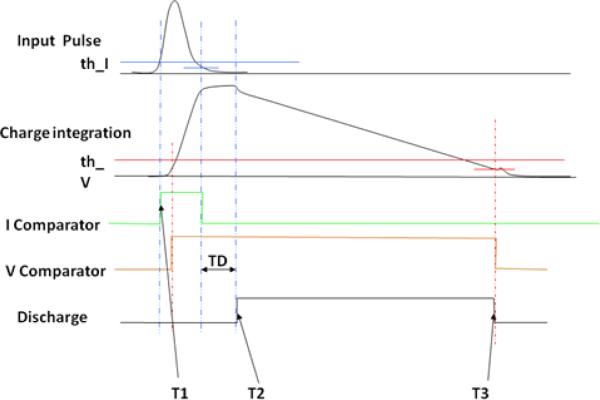
As shown in Fig. 1, the basic working principle of TBR can be described as following:
-
1)
TBR measures the signal timing in two steps: a) with a standard leading edge (LE) timing pickoff method, TBR applies an amplitude threshold (timing threshold) to the input signal to get an initial timing, t1; b) the walk error from LE due to different input signal amplitudes can be corrected with an accurately measured quantitative relationship between the t1 and its signal amplitude, which in principle is proportional to the value of total signal integration if the signal characteristic rise and fall time constants are the same. In this study, detector current output signals were used for the measurement. Therefore, the value of total signal integration is equivalent to the total collected charge, Q, which is proportional to total event energy as well.
-
2)Energy is measured in the following steps: a) TBR integrates the input signal over its waveform within two signal thresholds set at the signal rising and falling edges, with the values of these thresholds generally the same as that of the timing threshold. b) With a peak-holding technique, the total integrated signal (charge) value is held in a buffer for a predefined time period until timing t2. c) A discharging with a constant rate starts at t2 and lasting until t3, when the charge value drops to a minimal threshold set above the electronics noise. The measured time difference between t2 and t3, or (t3−t2), is used to directly calculate the total charge Q or energy:
where k is the discharging rate.(1) -
3)
A prior calibration that precisely measured t1 as a function of energy will be used to correct the variations of t1 from different energies.
Figure 1.
Circuit principle: 1) A leading edge current-threshold provides a timing pickoff from the input single pulse; 2) The charge of the input pulse is integrated between the two thresholds at the rise and fall pulse edges. 3) At the end of a peak holding with predefined time period TD, a discharge starts at a timing t2 and terminates at t3 determined by a voltage threshold.
In summary, TBR will convert the detector signals into three digital timing pulses of t1, t2, and t3 to measure the corresponding event energy and timing. These timing pulses can be easily generated through simple components such as comparators and be processed by either a TDC or FPGA with excellent accuracy.
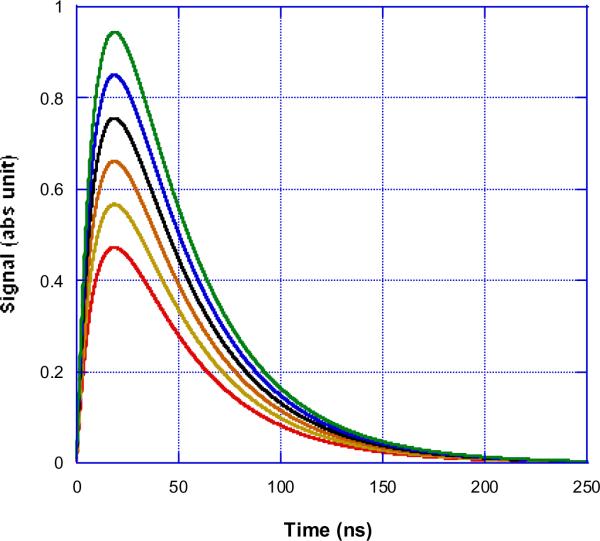
Numerical simulations have been conducted to demonstrate the timing measurement and correction by TBR with input signals of different amplitudes. Signals with six different amplitudes were simulated (Fig. 2), all with the same rise and fall time constants of 10 ns and 40 ns, respectively. By setting the timing threshold at a fixed signal level, different values of timing t1 were generated by the LE method from different signal amplitudes. The relationship between these different timing values and the corresponding integrated signal values at different threshold levels were calculated (Fig. 3). It is clear that one can easily correct the timing walk error once such a calibration is determined [7].
Figure 2.
Simulated signal pulses with different amplitudes. The characteristic rise and fall time constants are 10 ns and 40 ns, respectively.
Figure 3.
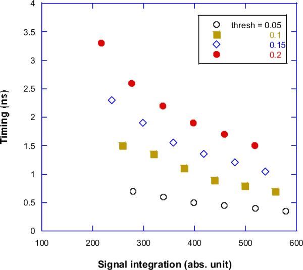
Timing with different signal amplitudes from leading edge thresholds as a function of different signal pulse integration values. Different threshold values were applied at the fraction of pulse amplitude. This validates that there is a sole numerical relationship between the timing and total integrated signal value.
In the above theoretical calculations, the origin of signal rise time was used as the time reference to calculate the relationship between the t1 and the signal integration (Fig. 3). In a real signal measurement, there is no such fixed time reference, because signals arrive at different moments of time. Therefore, a method is needed to provide a common time reference so that the time difference between this reference and t1 can be measured as a function of the signal integration values. The detailed experimental studies will be explained in section B.3.
In principle, the energy (total charge) measured by TBR is similar to that of Wilkinson ADC or PWM. However, TBR applies several techniques to improve the accuracy of energy measurement or to simplify the circuit design, as follows:
-
1)
An additional predefined timing t2 is introduced as the starting point of discharging, which makes it possible to measure the total charge directly without relying on the use of an analog CFD, which can be complicated to implement at the ASIC level and cumbersome to operate with a stringent requirement regarding its signal-dependent time delay.
-
2)
A constant current source is used to maintain a constant discharging rate so that linearity and stability can be significantly improved compared with PWM, which relies on a simple RC circuit to discharge.
In addition to simplified circuit design and reduced cost, TBR can in general further improve accuracy of timing measurement by applying sophisticated correction algorithms at the FPGA level with existing digital timing processes. Therefore, by achieving accurate measurement of energy and timing through entirely time-based pulses and processes, TBR is a promising readout method for PET detectors, in particular for those that demand large number of readout channels, high packing fraction, and high performance. With its simplified circuit and low cost, TBR is expected to be suitable for developing a parallel readout electronics that can independently read out and process signals from each individual detector channel. This can significantly improve the detector performance with an enhanced signal-to-noise ratio and increased capability to apply different event logic and signal processing algorithms.
2.2 Circuit design and implementation
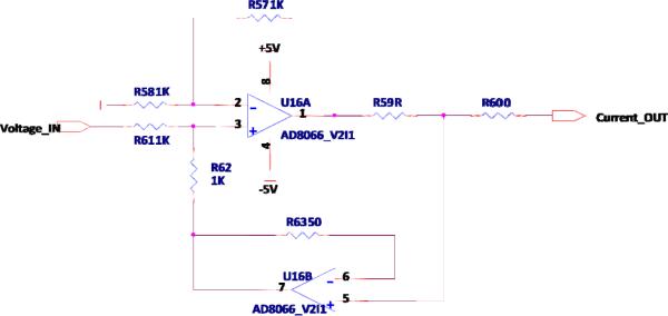
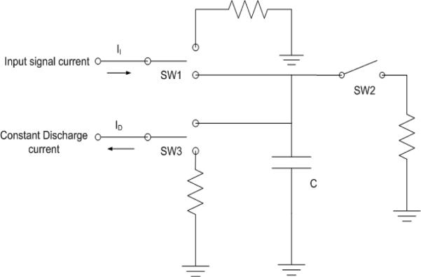
A test circuit with discrete components was designed and implemented to evaluate the feasibility and performance of TBR. This is a single channel circuit implemented on a four-layer PC board (Fig. 4). A voltage-to-current converter, as shown in Fig. 5, is used at the input stage so that either current or voltage input sources can be applied. Three comparators were used to generate digital timing pulses. An adjustable threshold is used to set the starting point of signal integration and generate the initial signal timing t1. Three switches were used in order to have well-separated stages of signal integration, discharge, and reset (Fig. 6).
Figure 4.
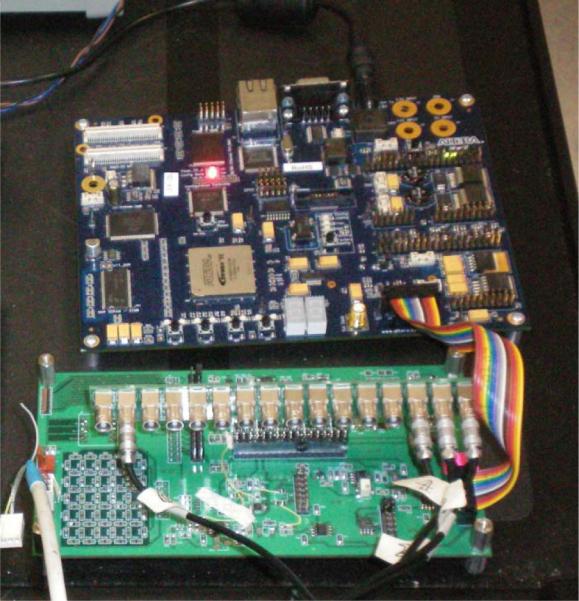
A photograph of TBR circuit with discrete components implemented on a PC board. It is connected to a FPGA board for signal control and processing.
Figure 5.
A circuit diagram of a voltage to current converter.
Figure 6.
A circuit diagram of three switches that were used for the charge integration (SW1), discharge (SW3) and reset (SW2) stages.
A second voltage-to-current converter is used to regulate a current source that controls the discharging rate. Compared with simple RC discharging [2], this circuit provides improved stability and accuracy of total signal energy measurement. Different discharging rates can be selected with a dip switch. Minimal errors in energy measurement can be achieved with a maximum (t3−t2) dynamic region. However, the selection of (t3−t2) dynamic region or discharging rate is related to the trade-off between the measurement accuracy and the overall discharging time that is associated with the detector counting-rate capability.
2.3 Experiment setup and measurement
An FPGA (Altera Stratix™ II) was used to control the converted digital timing pulses from TBR. The timing (t1) and energy (t3−t2) of these pulses were measured through two eight-channel CAMAC TDC modules (LeCroy 2228A and LeCroy 4208A) with 50 ps and 1.0 ns resolutions, respectively. Data were acquired in list mode and post-processed after acquisition.
The accuracy and linearity of pulse height measurement and the timing jitter caused by the electronics circuit were studied with input signals from a digital pulse generator (Agilent 33220A, 20-MHz DAC). The signal waveform from an LYSO/based detector was initially recorded with a digital oscilloscope (Tektronix 3034B) and then stored in the pulse generator to generate signals that mimic the real detected signals with different amplitudes.
Energy measurement
For the energy measurement study, we used a single-channel detector consisting of a 1 × 1 × 10 mm3 LYSO crystal optically coupled to a single-channel PMT (Hamamatsu R7400U), with all crystal sides except the end coupled to the PMT polished and wrapped with white Teflon tape. A Na-22 point source was used to irradiate the crystal with gamma photons. The signals from the PMT were split and fed to both TBR and a shaping amplifier (CAEN N568) with 1 μsec shaping time. The output of this shaping amplifier was connected to a standard CAMAC peak-sensing ADC (LeCroy 4208A) for energy measurement. With this setup, the results from two different methods could be compared. A common event trigger was generated by a minimal energy threshold and applied to both TBR and ADC.
In the data analysis throughout this study, the energy values measured from TBR were represented by (t3−t2) values since they differ only by a constant factor. The discharge rate was adjustable in the range of 0.0 – 1.2 mA, with a 0.3-mA increment value. The (t3−t2) values were in the range of 0.0 – 8.0 μsec, with a 1.0-ns bin size.
Timing measurement
The setup for the above energy measurement was expanded to measure the coincidence timing between two detectors. The schematic drawing of this timing measurement is shown in Fig. 7. A Na-22 point source was placed between the two detectors and used to irradiate the detectors for coincidence timing measurement. Both detectors were very similar to the one being used in the energy measurement, with each one consisting of a single 3 × 3 × 20 mm3 LYSO crystal optically coupled to a PMT (Hamamatsu R7400U). The signals from the first detector were split and fed to both a TBR and a CFD; the signals from the second detector were fed to a different CFD. With this setup, the coincidence timing resolutions measured from both CFD-CFD and CFD-TBR configurations could be compared. A NIM majority logic unit (Phillips Scientific 754) was used to generate a coincidence event trigger from two CFDs, with coincidence timing window set at 20 ns. The timing pulses from both detectors were measured by the same CAMAC TDC with 50-ps timing resolution.
Figure 7.
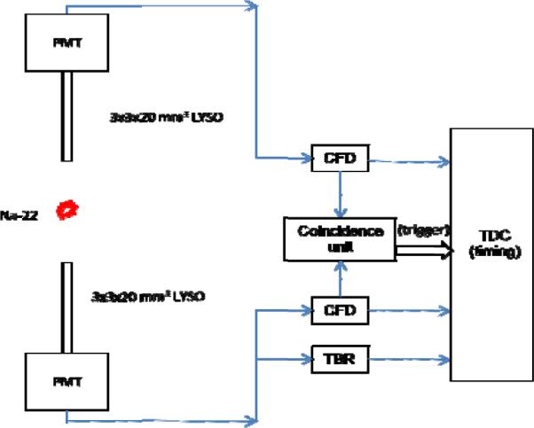
A schematic drawing of experimental setup for coincidence timing measurement.
The timing walk error from TBR was corrected based on the method described in section B.1. In a practical calibration, the timing t1 has to be measured against to a fixed time reference. In this study, the output trigger from the pulse generator was used as the time reference during the calibration. A simple experiment was conducted to measure the walk error due to different signal amplitudes. Test pulses from the pulse generator were split and fed to both a CFD and a TBR. As shown in Fig. 8, the means of coincidence timings measured from the CFD were almost the same, ranging from 1168 to 1197 ps, even for signals with different amplitudes since, as expected, the CFD corrected its walking errors. However, there were significant differences in the means of coincidence timing measured from a TBR for signals with different amplitudes, resulting from walk errors by LE timing pickoff.
Figure 8.
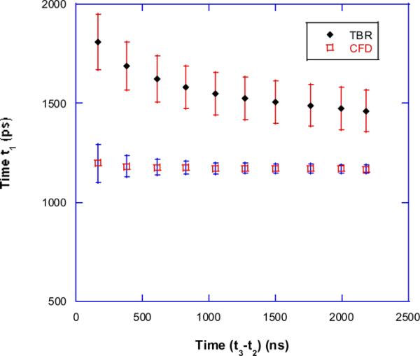
Timing walk errors with CFD and TBR: coincidence timings between a fixed pulse trigger and CFD or TBR were measured as a function of (t3−t2) acquired from TBR. Error bars (timing uncertainties) are described in more details in Figure 9.
In this study, the above calibration was measured with t1 as a function of (t3−t2). To correct the timing walk error, a correction factor determined from its corresponding (t3−t2) value and the calibration curve was applied to the value of a measured t1.
3 Results
3.1 Circuit basic performance
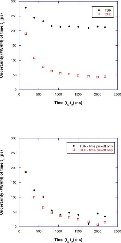
The uncertainty of timing measurement from TBR and CFD are shown in Fig. 9 (top). An overall value of less than 300 ps timing jitters was measured over a 10:1 dynamic range. This jitters value is small and can be neglected for a non-time-of-flight PET detector measurement. The timing jitters value measured from the CFD was significantly smaller than that measured from TBR, particularly at the larger signal amplitude region.
Figure 9.
Uncertainty of timing measurement (timing jitter): (top) the timing spread (FWHM) of t1 was measured as a function of (t3−t2) acquired from TBR and CFD, with their overall uncertainties less than 300 and 200 ps respectively over a 10:1 dynamic region; (bottom) the intrinsic timing spread by timing pickoff only was calculated by subtracting timing jitter caused by the electronic circuit components. The corresponding values from TBR and CFD are about the same.
These measured timing uncertainties are the combined effects from the timing pickoff of input pulse and the intrinsic timing variation and response of the electronics circuit. We noted that the timing jitters from both TBR and CFD reached different constant values when input pulse amplitudes became large. This is because while the intrinsic timing variation from the electronics circuit, Δtelec, is usually a constant for signals having the same rise time (and bandwidth) even with different amplitudes, the corresponding value of timing jitters from the timing pickoff, Δtpickoff, decreases with the increase of signal amplitude [8, 9]. Therefore, the asymptotic value of the timing jitters at large signal amplitudes measures the intrinsic timing variation of the electronics circuit itself. For the prototype TBR and the CFD used in this study, their corresponding Δtelec values were 209 and 42 ps, respectively, indicating that the circuit components of the prototype TBR were inferior to the commercial CFD components in terms of timing performance, and this was the dominating factor that caused the overall worse timing performance by TBR as shown in Fig. 9 (top). It can also be illustrated by the following: Δtelec and Δtpickoff can be reasonably assumed to be independent; then Δtpickoff can be calculated by subtracting Δtelec quadratically from the measured overall timing jitters. As shown in Fig. 9 (bottom), Δtpickoff calculated from both TBR and CFD are about the same, with a maximum difference of less than 37 ps. Therefore, if the intrinsic timing variation from the electronics circuit components can be improved (e.g., by using ASIC instead of discrete components implemented on a PCB), TBR can in principle provide a timing accuracy similar to that of a commercial CFD.
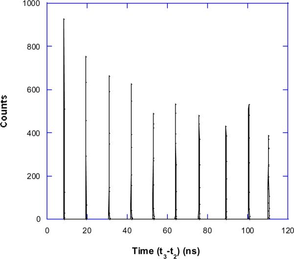
The accuracy of signal amplitude measurement is shown in Fig. 10. The output from TBR was measured in (t3−t2) with a constant discharging rate and minimal energy threshold applied to test pulses with different amplitudes. The measured spread of output values was very small, around 270 ± 50 ps, over a range from 8 to 110 ns. Because the corresponding (t3−t2) value of a minimal energy threshold was greater than 100 ns for a PET detector measurement, the contribution of this signal spread from circuit to the energy resolution was negligible.
Figure 10.
Accuracy of signal measurement: spectra of (t3−t2) measured from pulses with the same rise and fall time constants but different amplitudes. The timing spread from these pulses is 272 ± 51 ps.
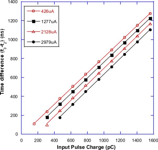
Fig. 11 shows that excellent linearity of signal measurement was achieved. When signals were applied with different threshold levels, their output values were correspondingly shifted, due to different signal integration values, but retained the same slope. Therefore, different threshold levels should not affect the accuracy of energy measurement.
Figure 11.
Linearity of signal measurement: time difference (t3−t2) measured as a function of input charge. Excellent linearity is shown for all measurements at different signal current threshold levels.
3.2 Energy measurement
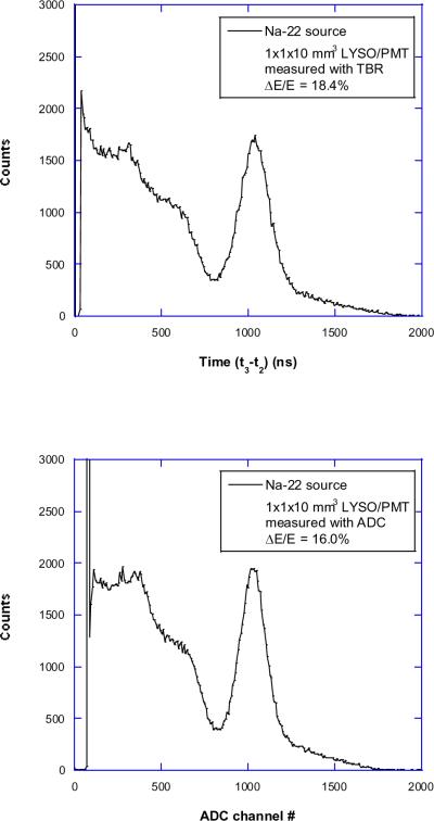
The energy spectra measured by TBR and ADC from a 1 × 1 × 10 mm3 LYSO are shown in Fig. 12. The corresponding energy resolutions based on a Gaussian curve fitting are ~18.4% and 16.0%, respectively. The energy resolution measured from ADC was better owing to the use of a shaping amplifier that improved signal-to-noise ratio. The bin size of (t3−t2) in this measurement was set to 1.0 ns, leading to a ~0.5 keV energy bin size.
Figure 12.
Energy spectra measured from a 1 × 1 × 10 mm3 LYSO/PMT detector with TBR (top) and ADC (bottom), with 18.4% and 16.0% resolutions with respect to their 511 keV photo-peaks, respectively.
3.3 Coincidence timing measurement
Fig. 13 shows the coincidence timing spectra measured between the two detectors. The measured timing resolutions (FWHM) with the CFD-CFD configuration were around 0.95 ns from all events and 0.83 ns from photo-peak events. Initial timing spectra measured with the CFD-TBR configuration without timing walk error correction are shown in Fig. 14, with degraded timing resolutions around 1.33 ns from all events and 0.95 ns from photo-peak events. A walk error correction was applied based on a calibration curve similar to that shown in Fig. 8, measured prior to the coincidence timing measurement. The corresponding corrected coincidence timing spectra are shown in Fig. 15, with improved timing resolution around 1.22 ns from all events and 0.95 ns from photo-peak events, which are very close to values measured from the CFD-CFD configuration.
Figure 13.
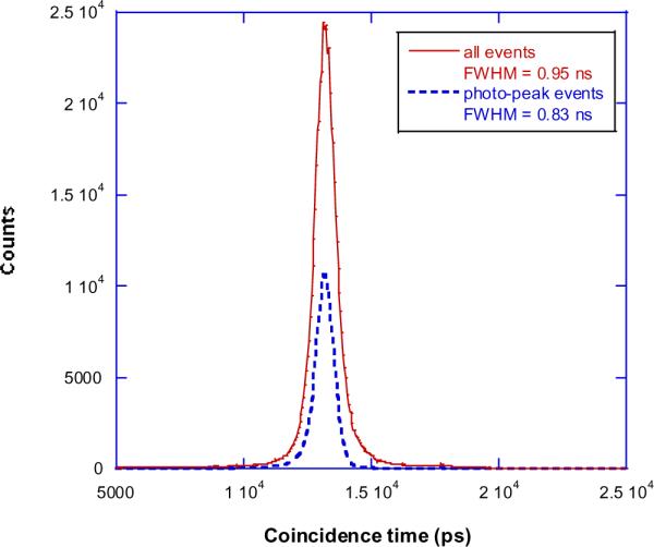
Timing spectra measured from a pair of 3 × 3 × 20 mm3 LYSO/PMT detectors with CFD-CFD timing pickoff configuration. The measured timing resolution (FWHM) is 0.95 ns from all events and 0.83 ns from photo-peak events (energy above 350 keV).
Figure 14.
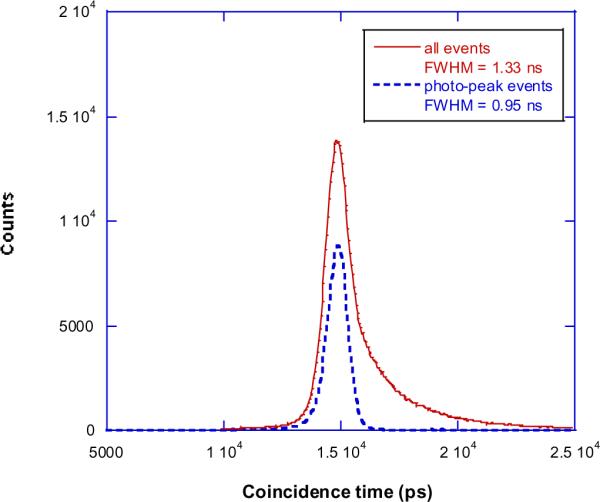
Timing spectra measured from a pair of 3 × 3 × 20 mm3 LYSO/PMT detectors with CFD-TBR timing pickoff configuration. Timing walk errors from TBR were not corrected. The measured timing resolution (FWHM) is 1.33 ns from all events and 0.95 ns from photo-peak events.
Figure 15.
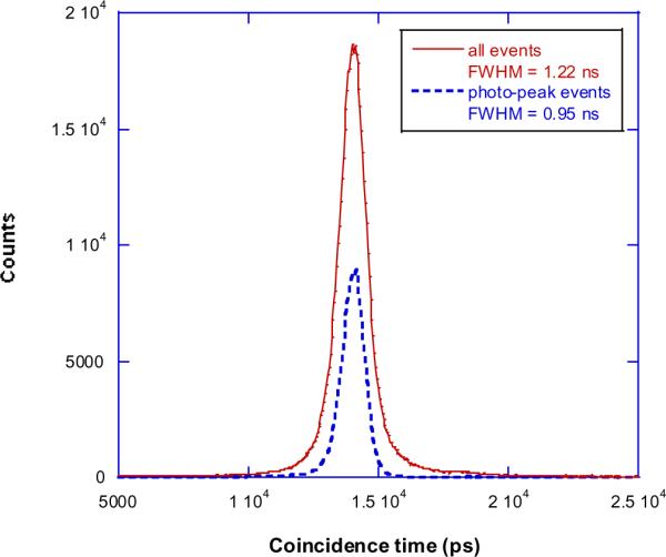
Timing spectra measured from a pair of 3 × 3 × 20 mm3 LYSO/PMT detectors with CFD-TBR timing pickoff configuration. Timing walk errors from TBR were corrected. The measured timing resolution (FWHM) is 1.22 ns from all events and 0.95 ns from photo-peak events.
4 Summary and Discussion
In this study, we developed and evaluated a new time-based detector readout method that can measure energy and timing accurately through time-based signals and processes. This initial study showed that accuracy and linearity of signal measurement, energy, and timing resolutions are well suited for most PET applications. Although this study used an external TDC to measure the timing signals, in principle all timing logic and data processing can be implemented at the FPGA level for achieving a compact data acquisition system.
The measurements demonstrated that the timing walk error from leading-edge timing pickoff can be effectively corrected based on a timing-amplitude calibration, yielding an improved accuracy of coincidence timing measurement with TBR. However, the measurements also showed that the timing resolution measured from TBR was worse than the one from CFD when all events were taken into account. This is mainly due to the fact that lower energy events had more significant deviation from the measured timing walk error function and led to larger errors after timing correction. Our results also showed that for PET coincidence event measurement the energy threshold is more effective than timing correction for improving timing resolution, with almost no difference between the two methods for photo-peak events. The reason is that timing walk error at the photo-peak energy level is much smaller than the timing spread attributed from other factors, such as limited photon statistics, photon sensor response, and noises. However, these studies were conducted with two specific detectors that were not optimal for timing measurement (although typical for non-time-of-flight PET applications). The timing performance of TBR for a sub-nanosecond application will need more careful studies.
The measured timing jitter of up to 300 ps was attributed mainly to uncertainty in the test pulse from a 20-MHz pulse generator, a relatively slow signal rise time (~40 ns), and stray capacitance from discrete circuit components connected to a PC board. This timing accuracy is not limited by the TBR method and can be significantly improved with ASIC and fast signal pulses. Therefore, in principle, TBR may be potentially applied to a time-of-flight PET.
There are many advantages of applying this time-based signal process to PET applications, including simplified circuit components, relatively low cost, easier implementation at ASIC level, and potentially enhanced performance through the power of FPGA with inherent digital timing processes. All these make TBR a suitable method for readout detectors that have a large number of channels with high packing fraction.
One potential limitation of TBR is its extended process time, which may reduce the counting rate to maximum of 0.1 – 1.0 MHz. However, TBR has a superior counting rate compared with free running ADC or other waveform sampling methods [1, 10]. In addition, because TBR will enable reading out of signals from each individual detector channel independently, the overall detector counting rate may not be degraded when compared with a conventional PET detector readout that combines signals from different channels. Additionally, the standard method of ADC and CFD has an extended processing time due to the signal shaping, and if the processing time of the TBR can be kept low, then even this limitation is minimal in comparison to current techniques. This type of study will be conducted in the next step with the implementation of TBR at the ASIC level.
5 Acknowledgments
This study was partially supported by award R21EB007581 from the National Institute of Biomedical Imaging and Bioengineering, and IRG from MD Anderson Cancer Center.
Footnotes
Publisher's Disclaimer: This is a PDF file of an unedited manuscript that has been accepted for publication. As a service to our customers we are providing this early version of the manuscript. The manuscript will undergo copyediting, typesetting, and review of the resulting proof before it is published in its final citable form. Please note that during the production process errors may be discovered which could affect the content, and all legal disclaimers that apply to the journal pertain.
6 References
- 1.Streun M, Brandenburg G, Larue H, et al. A PET system with free running ADCs. Nucl. Instr Meth Phy. Res. A. 2002;486:18. [Google Scholar]
- 2.Olcott PD, Levin CS. Pulse width modulation: a novel readout scheme for high energy photon detection. IEEE Nuclear Science Symposium Conference Record.2008. [Google Scholar]
- 3.Meyer TC, Powolny F, Anghinolfi F, et al. A time-based front end readout system for PET & CT. IEEE Nuclear Science Symposium Conference Record.2006. [Google Scholar]
- 4.Yousif AS, Haslett JW. A Fine Resolution TDC Architecture for Next Generation PET Imaging. IEEE Trans. Nucl. Science. 2007;54:1574. [Google Scholar]
- 5.Powolny F, Auffray E, Hillemanns H, et al. A Novel Time-Based Readout Scheme for a Combined PET-CT Detectors Using APDs. IEEE Trans. Nucl. Science. 2008;55:2465. [Google Scholar]
- 6.Yousif AS, Haslett JW. Time-based ADC and TDC architectures. CMOS Emerging Technology Workshop, 2008. 2008 http://www.cmoset.com/uploads/11A.3-08.pdf.
- 7.Kichimi H, Yoshimura Y, Browder T, et al. The BELLE TOF System. Nucl. Instr. Meth. Phy. Res. A. 2000;453:315. [Google Scholar]
- 8.Nicholson PW. Nuclear Electronics. John Wiley & Son; New York: 1974. [Google Scholar]
- 9.Leo WR. Techniques for Nuclear and Particle Physics Experiments. 2nd ed. Springer-Verlag; New York: 1994. [Google Scholar]
- 10.Ruckman LL, Varner GS. Sub-10 ps monolithic and low-power photodetector readout. Nucl. Instr. Meth. Phy. Res. A 2009. 2009;602:438. [Google Scholar]


