Abstract
Effect of different aspect ratio (length to diameter ratio, L:D) on single polypyrrole (Ppy) nanowire based field effect transistor (FET) sensor for real time pH monitoring was studied. Ppy nanowires with diameters of ~60, ~80 and ~200 nm were synthesized using electrochemical deposition inside anodized aluminium oxide (AAO) template and were assembled using AC dielectrophoretic alignment followed by maskless anchoring on a pair of gold electrodes separated with different gap lengths. Microfabricated gold electrode patterns with gap size between 1 - 4 μm were developed by means of MEMS technique (photolithography). Using field effect transistor geometry with pair of microfabricated gold contact electrodes serving as a source and a drain, and a platinum (Pt) mesh (anchored in a microfluidic channel) was used as a gate electrode. When effect of different aspect ratio of the nanowire were compared, higher sensitivity was recorded for higher aspect ratio. The sensitivity was further improved by modulating the gate potential. These FET sensors based on single polypyrrole nanowire exhibited excellent and tunable sensitivity towards pH variations.
Keywords: Polypyrrole, single nanowire, real-time sensing, aspect ratio, field effect transistor, microfluidics, pH sensor
Introduction
Polypyrrole is a versatile organic semiconductor with a high technological potential. Over other semiconductors, Ppy has two main advantages i.e. low electropolymerization potential which allows film formation in water as well as stability under ambient conditions [1, 2]. Applications of Ppy as the active medium in various sensors have been demonstrated, e.g., in gas detectors for NH3, NO2, or H2S, [3, 4] or as biosensors using enzymes and antibodies as recognition biomolecules [5-8]. One-dimensional (1D) nanostructures including nanowires, nanorods, nanobelts and nanotubes, have attracted much attention because of their fundamental significance in chemistry, physics, materials science and engineering and potential application in nanoelectronics [9-12]. As semiconductor nanowires assumed important roles in electronic and optoelectronic nanodevices, rational control over their morphology, structure and key properties became increasingly important [10, 13-16]. Electronic conduction in nanowires takes place by bulk conduction due to their high density of electronic states, diameter-dependent band gap, enhanced surface scattering of electrons and phonons, increased excitation/binding energy, high surface to volume ratio and large aspect ratio. As a result, nanowires exhibit unique electrical, magnetic, optical, thermoelectric and chemical properties [17, 18].
The use of conducting polymer nanowires for biosensing application, however, has been limited due to their incompatibility with traditional microfabrication processes such as lithography and focused ion beam (FIB) owing to its possible thermal damage during these processes [19, 20]. Simpler and less costly method of assembling conducting polymer nanowire devices have relied on bottom-up geometry in which nanowires are deposited on the top of prefabricated electrodes. A limitation of this method is the difficulty in eliminating the change in contact resistance due to physical disturbances/movements introduced during liquid phase sensing. Also, to achieve sensor to sensor reproducibility, it is necessary to have precise number of individual nanowires electrically connected between the electrodes, which is lacking during drop casting method of fabrication [19]. To address these issues we have developed a simple and cost-effective all electrochemical approach to fabricate, assemble and anchor single conducting polymer (polypyrrole, Ppy) nanowire [21].
It has been shown that there is a significant impact of the dimensions of the semiconducting channel on the device performance [22, 23]. For example, diameter has been shown to affect the field effect transistor performance of carbon nanotube devices [24]. In an another report, the length of the metallic CNT has been shown to affect not only the transfer characteristics but also breakdown voltage and current carrying capacity of the device [25]. However, direct impact of these parameters on the applications such as sensitivity of the sensor has not been systematically evaluated. To understand the role of these physical dimensions of the device, aspect ratio (length to diameter ratio, L:D) can be a better benchmark to compare device to device performance variation. To date very limited understanding has been developed amongst scientific community about the effect of aspect ratio of the nanostructures on the device sensitivity which can potentially assist in improving the device performance. Also for higher selectivity and higher sensitivity, it is important to have the ability to detect low concentration of specific analytes. Higher selectivity can be achieved by tuning or modifying the chemical and physical properties of conducting polymer nanowire. While higher sensitivity can be achieved by operating the sensors as field-effect transistors (FETs) because of the ability of FET to amplify in-situ and to gate-modulate channel conductance. As well as FET-based sensors are compatible with well-developed microelectronic fabrication techniques which are useful in device miniaturization, high density array fabrication and require small sample volumes (advantageous for biosensing). Also nanowire FETs have been of particular interest in the past several years, motivated by both the necessary investigations of basic carrier-transport behaviour in nanowire and the promise of future high-performance FET devices. [26-29].
Thus, we are reporting the effect of aspect ratio of single Ppy nanowire FET in details with regards to its pH sensing and gate potential controlled sensitivity modulation. To the best of our knowledge, this is the first systematic study of the effect of aspect ratio (L:D) (~60, ~80, ~200 nm in diameter and the length of ~1 to 4 μm) on the sensing performance of a single Ppy nanowire based FET device.
Experimental details
Chemicals and reagents
Pyrrole (Ppy) (Sigma-Aldrich, St. Loius, MO), lithium perchlorate (LiClO4) (Aldrich, Milwaukee, WI, USA), sulphuric acid (H2SO4), hydrogen peroxide (H2O2), pH buffer solution (1-11) (Fisher Scientific,Fair Lawn, New Jersey, USA), tetrachloroauric acid (HAuCl4) (Technic Inc), phosphoric acid (Acros organic), were used in the present study. All the reagents were prepared in nanopure water.
Polypyrrole nanowire synthesis
Polypyrrole nanowires were electrochemically synthesized using well established template directed electrodeposition technique [30, 31]. Alumina membrane of 200 nm pore size and 60 μm thickness (Whatman International Ltd, Maidstone, England) and the alumina membranes with ~60 & ~80 nm pore diameter (synthesized in the laboratory [32], Parameters : 1.27 mm thick aluminium foil, 0.3 M Oxalic acid, 50 V, 20° C for 12 hr) were used as scaffolds for nanowire fabrication. Seed layer was deposited by sputtering ~200 nm thick gold using the Emitech K550 (Emitech Ltd., Kent, England) sputter coater on one side of the alumina template. Pyrrole (0.5 M), LiClO4 (0.2 M) was used as electrolyte solution. Chronocoulometry method (CHI Electrochemical Analyzer) was used for electrodepositing Ppy nanowires by passing 0.7 C charge at 0.9 V vs Ag/AgCl. The gold seed layer was removed using 0.15 M KI in 0.1 N I2 gold-etchant solution. After washing with water, the alumina template was dissolved in 30% H3PO4 acid and briefly sonicated to free the nanowires and form a uniform suspension. Nanowires were washed and resuspended in nanopure water. The suspension was diluted 10-fold for further use.
Fabrication of single Ppy nanowire FET device
A (100) oriented silicon wafer consisting of 16-pairs of ~55 μm rectangular gold electrodes with 1 – 4 μm gap and separated by ~70 μm was used in this work. The gold electrodes, patterned by standard lift-off photolithography technique, were made up of 200 A0 chromium (Cr) adhesion layer and 1800 A0 thick gold (Au) contact layer The electrodes were cleaned with piranha solution (3.5 ml 98% H2SO4 + 1.5 ml 30% H2O2). To prepare single Ppy nanowire devices, the two sides of 16-pairs were shorted to form two terminals followed by applying an alternating current field of 5 MHz frequency and 3 V peak to peak voltage between the two terminals. A 2 μl drop of Ppy nanowire suspension was dispensed on it and alignment was carried out till the drop was completely evaporated. To achieve single nanowire connection between a pair of contact electrodes, excess nanowires were physically/manually removed using a probe tip made out of 25 μm diameter gold wire under a 1000x magnification optical microscope. In order to secure the Ppy nanowire on to the gold electrodes, the nanowire was anchored with maskless electrodeposition, using chronoamperometry method (CHI Electrochemical Analyzer). A three electrodes configuration electrochemical cell consisting of the 16-pairs of contact electrodes with single Ppy nanowire connections as the working electrode, Ag/AgCl as a reference electrode and a platinum coated metal strip as a counter electrode were used. The electrolyte used was Technigold (Technic Inc., California, USA) at pH of 7.0 and the deposition potential used was -0.5 V vs Ag/AgCl at room temperature for 10 min for the built up of ~300 nm thick gold layer on the gold electrode surface.
Microfluidic Channel Fabrication
Microfluidic channel was fabricated using solution of 10:1 ratio of Silicon Elastomer base to the curing agent (Dow Corning Co. Midland, USA). The solution was degassed under vacuum for 1 hr to remove any bubbles. Then the solution was poured in a microfluidic mould containing Pt mesh and the polymer was cured at 145° C for 1 hr. Pt mesh was physically pressed down on to the mould to ensure part of it was exposed in the final microfluidic channel which acted as an electrolyte/ion gate electrode.
Sensing Measurements
For sensing, standard pH buffers (1 – 11 pH) (procured from Fisher Scientific) were used. For real time pH sensing, 500 μl/min sample flow rate was maintained through the microfluidic channel. Response of the sensor was recorded using Agilent 4155A semiconductor parameter analyzer. FET studies were carried out by measuring source drain current (IDS) flowing through the nanowire while keeping source drain bias voltage (VDS) at 0.5 V with varying gate potentials (VG).
Results and Discussion
To study different aspect ratio, Ppy nanowire of varying diameters were synthesized by electrodeposition in different pore diameter AAO templates and then assembled on prefabricated gold microelectrodes with different gap size. Figure 1 shows the SEM images of anchored single Ppy nanowire on a pair of gold electrodes with varing aspect ratio. Figures 2 (a) and 2(b) show the schematic of the microfluidic channel assembled on a single Ppy nanowire device in which the two gold electrodes served as the source and the drain while the Pt mesh anchored in the microfluidic channel served as the electrolyte/liquid ion gate and an optical image of microfluidic assembled single Ppy nanowire anchored on a 16 electrode pattern chip, respectively. These devices were characterized in terms of their pH sensitivity and FET characteristics.
Figure 1.
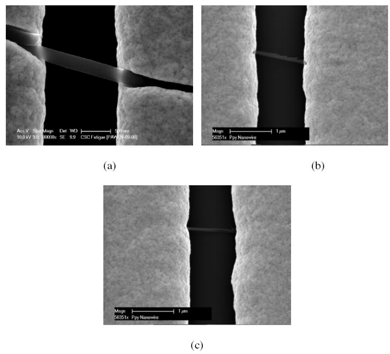
SEM images of single Ppy nanowire based devices with different aspect ratio (L:D) (a) L:D = 1.5:0.246, (b) L:D = 1.43:0.083 (c) L:D = 1.3:0.064 (dimensions in μm).
Figure 2.
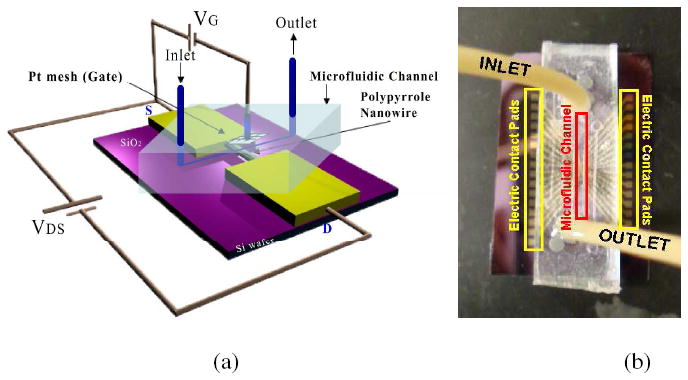
a) Schematic of single Ppy nanowire FET device and b) photo-image of a microfluidic assembled FET device.
Effect of Aspect Ratio (L:D)
Figure 3 (inset) shows the real time pH sensing response of a single Ppy nanowire FET device. Fourteen different (L:D) aspect ratios (Ppy nanowire with ~60, ~80 and ~200 nm in diameter and ~1 to 4 μm in length), at a constant gate potential of VG = 0 V (no gate applied), were studied for their pH responses. Their respective calibration plots are presented in figure 3. Change in the IDS with respect to reference IDS0 (IDS at pH = 10) value of single Ppy nanowire was observed with changing the pH value from 1 to 10, and it was found that ΔIDS/IDS0 decreases with increasing pH value. The decrease in IDS with increase in pH is a result of the lower conductivity of the polymer in less acidic media. The dependence of conductivity on pH is attributed to the protonation/deprotonation of the pyrolitic unit in Ppy nanowire [33]. Protonation (due to decrease in pH) results in the formation of delocalized radical cations and is accompanied by an increase in the conductivity or decrease in the resistance. This trend was similar for all aspect ratio, with varying sensitivity.
Figure 3.
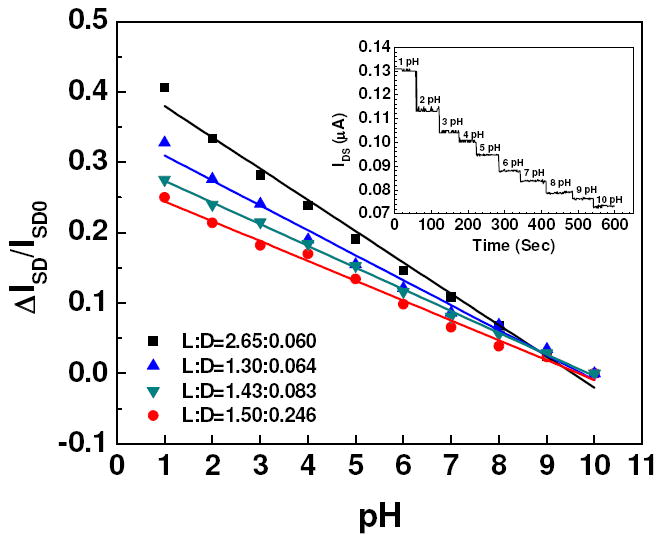
pH calibration curve of single Ppy nanowire for four representative aspect ratio (L:D, microns) at VG = 0 V with VDS = 0.5 V. Solid lines represent the best linear fit for the data points. (Inset) Real-time pH sensing response of a single Ppy nanowire device.
Figure 4 shows the sensitivity of single Ppy nanowire for different aspect ratio (L:D) at VG = 0 V and VDS = 0.5 V. Sensitivity was calculated as the slope of the pH calibration curve (from Figure 3) for each aspect ratio. Higher sensitivity was observed with increasing L:D aspect ratio, which implied that lower diameter and longer length of Ppy nanowire recorded higher sensitivity. As the diameter of the nanowire decreases, the number of surface atoms greatly increases. The large surface to volume ratio of nanowire could change the conducting properties that are largely determined by the number of surface atoms. Conductance in a small diameter nanowire is related to the sum of electron transport in conduction channels and it is defined by their quantization energy. This means, thinner the wire, smaller the available unaffected volume, and hence smaller the probability of uninterrupted conduction [34, 35]. On the basis of surface to volume ratio, Niklas Elfström et. al. [36] argued that an increased sensitivity for surface charges for smaller widths should be reflected in a difference in the threshold voltage with respect to width. Also the surface charge is enhanced when the width of the nanowire is decreased. It can also be seen from Figure 4 (inset), that the sensitivity is a function of sensor surface area. Increase in the sensitivity was observed with increase in the sensor surface area. However different rates of increase in the sensitivity was observed for different Ppy nanowire diameter. Smaller diameter of the wire has curt change in the sensitivity curve as a function of surface area compared to the bigger diameter. Similar observation was made for carbon nanotube based devices for their FET performance, wherein device ‘ON’ current had much higher dependence on CNT diameter at smaller diameter range than at bigger end of the range [25]. We also observed higher sensitivity for higher lengths, as the higher length may provide more room for binding the analyte on the nanowire resulting in the higher sensitivity.
Figure 4.
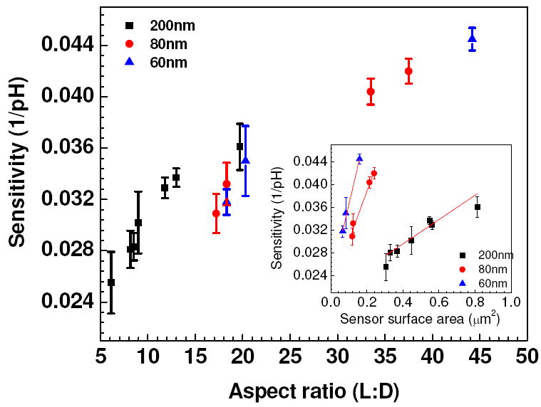
Sensitivity vs aspect ratio (L:D) plot of single Ppy nanowire FET devices and (Inset) relationship between sensitivity vs surface area of single Ppy nanowire for different diameters.
Effect of Gate Voltage (Vg)
The electrical characteristics of single Ppy nanowire FET device were studied by monitoring IDS while sweeping gate voltage at a fixed value of VDS = 0.5 V. Transistor performance was evaluated by calculating the transconductance (gm) and the on/off current ratio (Ion/Ioff). Figure 5 shows IDS vs gate potential (VG) response of a single Ppy nanowire FET device for various pH. IDS was negligible for negative gate voltages for the pH ranging from 1 to 8 indicating that the device was in off state as Ppy was in the reduced state and therefore insulating. However, increase in IDS was observed for more positive gate potential implying ON state of the device [37]. Increasing the VG to more positive potential had the effect of oxidizing the nanowire resulting in a gradual increase in IDS to a maximum at 0.8 V. Further increase of VG resulted in a decrease of IDS as the nanowire was fully oxidized (data not shown). Significant increase in the IDS was observed for both positive gate voltages as well as negative gate voltages for pH range of ~ 9 – 11. This clearly indicates that, an increase in the IDS under negative gate modulation is due to hole conduction and it is due to the electron conduction under positive gate modulation [38]. Transconductance of the Ppy nanowire FET was obtained from the slope of the linear region in the IDS vs VG plot (Figure 5) in the positive gate potential range (oxidized state of the polymer). It was about 0.86 μS/μm for pH 1, which is higher than reported earlier [33], and this value steadily decreased to 0.23 μS/μm for pH 11. Similar calculations of transconductance in the negative gate potential range (reduced state of the polymer) revealed a reverse trend in the values. Transconductance values varied from almost zero (+0.08 nS/μm) at pH 1 to -0.10 μS/μm at pH 11. The maximum ratio of IDS at saturation (Ion) at VG = 0.8 V to minimum IDS at depletion (Ioff) (at VG ~ -0.1 to -0.4 V) for FETs based on single Ppy nanowire was ~274 at pH 1, which was 2-3 times better than conducting polymer nanowire electrode junction transistors (CPNEJ-FETs) [38], and showed a steady decline to on/off ratio of ~78 at pH 11. Thus, from ISD-VG curve (Figure 5) for the single Ppy nanowire device it was clearly understood that the gate voltage controlled oxidation/reduction states of the conducting polymer nanowire showed different sensitivity towards same range of pH.
Figure 5.
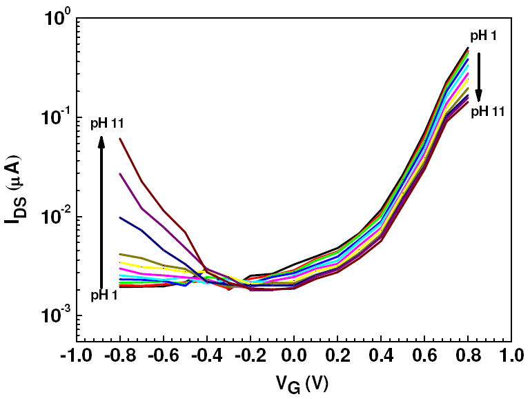
IDS vs VG curves of a Ppy nanowire FET device in different pH. Direction of the arrow indicates the pH change from 1 to 11 in steps of single pH unit change (VDS = 0.5 V).
So in order to study the effect of different VG in detail, we applied VG = 0.2 V, 0.8 V (oxidized state) and -0.8 V (reduced state) at VDS = 0.5 V and studied response of nanowire FETs with different aspect ratio. Figure 6 shows the real time pH sensing response of a Ppy nanowire FET device at a constant gate potential of VG = 0.8 V and 0.2 V. The calibration plot of Ppy nanowire FET device is shown in Figure 6 (inset). Sensitivity improved when gate potential was increased from 0.2 V to 0.8 V for fixed aspect ratio of the nanowire as well as with increasing aspect ratio at the same gate potential as can be seen from figure 7. When compared, the sensitivity at positive VG voltages was higher when compared with VG = 0 V (no VG) applied (Figure 4). Figure 8 shows the real time pH sensing and the calibration plot (inset) of a Ppy nanowire FET device for constant VG = - 0.8 V (reduced state). We observed extremely small response at VG = - 0.8 V for pH range from 1 to 8 as compared to VG = 0.8 V. Slight increase in ISD was observed for the pH range from 1 to 8, however, significant increase was observed for pH > 8. This reverse response at very high pH, though not completely understood, could arise due to the hole carrier modulation brought about in a reduced polymer nanowire.
Figure 6.
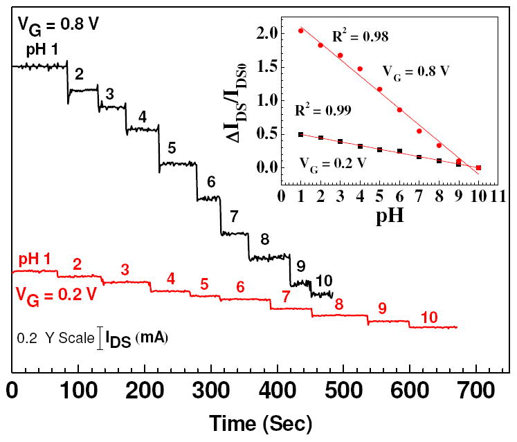
Real-time response for IDS flowing through Ppy nanowire at various pH values as a function of gate potential VG = 0.8 V & 0.2 V at VDS = 0.5 V. (Inset) ΔIDS/IDS0 vs pH calibration curve of Ppy nanowire FET device for aspect ratio (L:D = 2.19:0.215) with solid line representing the best linear fit along with their respective regression coefficients (R2).
Figure 7.
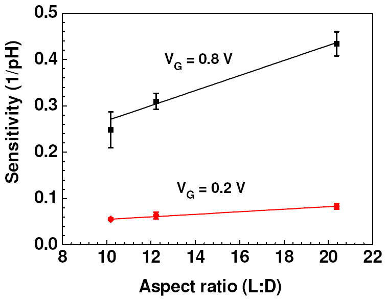
Sensitivity vs aspect ratio (L:D) curve of single Ppy nanowire FET devices at VG = 0.2 V and 0.8 V. Solid line represents the best linear fit.
Figure 8.
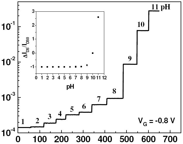
Real time response of IDS flowing through Ppy nanowire at various pH values and (Inset) ΔIDS/IDS0 vs pH calibration plot at gate potential of VG = -0.8 V for aspect ratio of L:D = 2.19:0.215.
Conclusion
We have successfully fabricated single conducting polymer (polypyrrole) nanowire based FET devices with different aspect ratio (L:D). We demonstrated the effect of aspect ratio on the sensitivity of single Ppy nanowire FET device by modulating diameter (i.e. ~60, ~80 and ~200 nm) and length (ranges from 1 - 4 μm) of Ppy nanowire. Electrolyte-gated FET structure was used to study and control the device properties. These devices also showed excellent FET properties with very high transconductance and on/off ratio indicating excellent gate voltage controlled ON (oxidized) or OFF (reduced) state of the polymer. For these devices, gate potential controlled sensor response modulation towards different pH was observed. Sensor showed higher sensitivity at more positive VG (0.8 V), where polymer is in oxidized state compared to lower VG (0.2 V) values or no gate potential applied. Completely reverse response was observed for VG of -0.8 V where polymer is in reduced state. These devices showed higher sensitivity for lower diameter and higher length (higher aspect ratio (L:D)) with or without the application of gate potential. These findings indicate that the conducting polymer nanowire FET sensors offer tunable sensitivity which can have a very big impact in the field of chemical and bio-sensing applications. Moreover, conducting polymer nanowires have great potential in 1-D-based FET technology due to their excellent electrical, optical properties and biocompatibility.
Acknowledgments
We acknowledge the support of grants CBET-0617240 from NSF, GR-83237501 from the U.S. EPA and U01ES016026 from NIH.
References
- 1.Asavapiriyanont S, Chandler GK, Gunawardena GA, Pletcher D. J Electoanal Chem. 1984;177:229–244. [Google Scholar]
- 2.Kanazawa KK, Diaz AF, Gill WD, Grant PM, Street GB, Gardini GP, Kwak JF. Synth Met. 1980;1:329–336. [Google Scholar]
- 3.Zhang J, Wang S, Xu M, Wang Y, Xia H, Zhang S, Guo X, Wu S. J Phys Chem C. 2009;113:1662–1665. [Google Scholar]
- 4.Geng L, Huang X, Zhao Y, Li P, Wang S, Zhang S, Wu S. Solid-State Electronics. 2006;50:723–726. [Google Scholar]
- 5.Cosnier S. Appl Biochem Biotech. 2000;89:127–138. doi: 10.1385/abab:89:2-3:127. [DOI] [PubMed] [Google Scholar]
- 6.Alaejos MS, Montelongo FJG. Chem Rev. 2004;104:3239–3266. doi: 10.1021/cr0304471. [DOI] [PubMed] [Google Scholar]
- 7.Sassolas A, Leca-Bouvier BD, Blum LJ. Chem Rev. 2008;108:109–139. doi: 10.1021/cr0684467. [DOI] [PubMed] [Google Scholar]
- 8.Pandey P, Singh SP, Arya SK, Gupta V, Datta M, Singh S, Malhotra BD. Langmuir. 2007;23:3333–3337. doi: 10.1021/la062901c. [DOI] [PubMed] [Google Scholar]
- 9.Lieber CM, Wang ZL. MRS Bull. 2007;32:99–108. [Google Scholar]
- 10.Li Y, Qian F, Xiang J, Lieber CM. Mater Today. 2006;9:18–27. [Google Scholar]
- 11.Duan X, Huang Y, Cui Y, Wang J, Lieber CM. Nature. 2001;409:66–69. doi: 10.1038/35051047. [DOI] [PubMed] [Google Scholar]
- 12.Huang HM, Mao S, Feick H, Yan H, Wu Y, Kind H, Weber E, Russo R, Yang P. Science. 2001;292:1897–1899. doi: 10.1126/science.1060367. [DOI] [PubMed] [Google Scholar]
- 13.Schoen DT, Xie C, Cui Y. J Am Chem Soc. 2007;129:4116–4117. doi: 10.1021/ja068365s. [DOI] [PubMed] [Google Scholar]
- 14.Yang HH, Zhang SQ, Tan F, Zhuang ZX, Wang XR. J Am Chem Soc. 2005;127:1378–1379. doi: 10.1021/ja0467622. [DOI] [PubMed] [Google Scholar]
- 15.Persson AI, Larsson MW, Stenstrom S, Ohlsson BJ, Samuelson L, Wallenberg LR. Nat Mater. 2004;3:677–681. doi: 10.1038/nmat1220. [DOI] [PubMed] [Google Scholar]
- 16.Tolani SB, Craig M, DeLong RK, Ghosh K, Wanekaya AK. Anal Bioanal Chem. 2009;393:1225–1231. doi: 10.1007/s00216-008-2556-0. [DOI] [PubMed] [Google Scholar]
- 17.Sarkar J, Khan GG, Basumallick A. Bull Mater Sci. 2007;30:271–290. [Google Scholar]
- 18.Sirbuly DJ, Law M, Yan H, Yang P. J Phys Chem B. 2005;109:15190–15213. doi: 10.1021/jp051813i. [DOI] [PubMed] [Google Scholar]
- 19.Yoon H, Kim J-H, Lee N, Kim B-G, Jang J. Chem Bio Chem. 2008;9:634–641. doi: 10.1002/cbic.200700660. [DOI] [PubMed] [Google Scholar]
- 20.Hangarter CM, Bangar M, Hernandez SC, Chen W, Deshusses MA, Mulchandani A, Myung NV. Appl Phys Lett. 2008;92:073104. [Google Scholar]
- 21.Bangar MA, Shirale DJ, Chen W, Myung NV, Mulchandani A. Anal Chem. 2009;81:2168–2175. doi: 10.1021/ac802319f. [DOI] [PubMed] [Google Scholar]
- 22.Im Y, Vasquez RP, Lee C, Myung N, Penner R, Yun M. J Phys: Conf Ser. 2006;38:61–64. [Google Scholar]
- 23.Al-Kaysi RO, Ghaddar TH, Guirado G. J of Nanomaterials. 2009;2009:436375. [Google Scholar]
- 24.Chen Z, Appenzeller J, Knoch J, Lin Y-M, Avouris P. Nano Lett. 2009;5:1497–1502. doi: 10.1021/nl0508624. [DOI] [PubMed] [Google Scholar]
- 25.Javey A, Guo J, Paulsson M, Wang Q, Mann D, Lundstrom M, Dai H. Phys Rev Lett. 2004;92:106804. doi: 10.1103/PhysRevLett.92.106804. [DOI] [PubMed] [Google Scholar]
- 26.Lin C-H, Hung C-H, Hsiao C-Y, Lin H-C, Ko F-H, Yang Y-S. Biosensors and Bioelectronics. 2009;24:3019–3024. doi: 10.1016/j.bios.2009.03.014. [DOI] [PubMed] [Google Scholar]
- 27.Wang D, Wang Q, Javey A, Tu R, Dai H, Kim H, McIntyre PC, Krishnamohan T, Saraswat K. Appl Phys Lett. 2003;83:2432. [Google Scholar]
- 28.Wang D, Chang Y, Wang Q, Cao J, Farmer DB, Gordon RG, Dai H. J Am Chem Soc. 2005;126:11602–11611. doi: 10.1021/ja047435x. [DOI] [PubMed] [Google Scholar]
- 29.Cui Y, Zhong Z, Wang D, Wang WU, Lieber CM. Nano Lett. 2003;3:149–152. [Google Scholar]
- 30.Xu Q, Meng G, Han F, Zhao X, Kong M, Zhu X. Materials Letters. 2009;63:1431–1434. [Google Scholar]
- 31.Hulteen JC, Martin CR. J Mat Chem. 1997;7:1075–1087. [Google Scholar]
- 32.Myung NV, Lim J, Fleurial J-P, Yun M, West W, Choi D. Nanotechnology. 2004;15:833–838. [Google Scholar]
- 33.Wanekaya AK, Bangar MA, Yun M, Chen W, Myung NV, Mulchandani A. J Phys Chem C. 2007;111:5218–5221. [Google Scholar]
- 34.Grieshaber D, MacKenzie R, Vörös J, Reimhult E. Sensors. 2008;8:1400–1458. doi: 10.3390/s80314000. [DOI] [PMC free article] [PubMed] [Google Scholar]
- 35.Tilke AT, Simmel FC, Lorenz H, Blick RH, Kotthaus JP. Phys Rev B. 2003;68:075311. [Google Scholar]
- 36.Elfström N, Juhasz R, Sychugov I, Engfeldt T, Karlström AE, Linnros J. Nano Lett. 2007;7:2608–2612. doi: 10.1021/nl0709017. [DOI] [PubMed] [Google Scholar]
- 37.He HX, Li XL, Tao NJ, Nagahara LA, Amlani I, Tsui R. Phys Rev B. 2003;68:045302. [Google Scholar]
- 38.Alam MM, Wang J, Guo Y, Lee SP, Tseng H-R. J Phys Chem B. 2005;109:12777–12784. doi: 10.1021/jp050903k. [DOI] [PubMed] [Google Scholar]


