

Abstract
Neural electrodes are essential tools for the study of the nervous system and related diseases. Low electrode impedance is a figure of merit for sensitive detection of neural electrical activity and numerous studies have aimed to reduce impedance. Unfortunately, most of these efforts have been tethered by a combination of poor functional coating adhesion, complicated fabrication techniques, and poor fabrication repeatability. We address these issues with a facile method for reliably producing multiple-electrode arrays with low impedance by patterning highly adherent nanoporous gold films using conventional microfabrication techniques. The high surface area-to-volume ratio of self-assembled nanoporous gold results in a more than 25-fold improvement in the electrode-electrolyte impedance, where at 1 kHz, 850 kΩ impedance for conventional Au electrodes is reduced to 30 kΩ for nanoporous gold electrodes. Low impedance provides a superior signal-to-noise ratio for detection of neural activity in noisy environments. We systematically studied the effect of film morphology on electrode impedance and successfully recorded field potentials from rat hippocampal slices. Here, we present our fabrication approach, the relationship between film morphology and impedance, and field potential recordings.
1. Introduction
Planar multiple-electrode arrays (MEAs) have become a widely used tool in neuroscience [1–3]. Planar MEAs are typically employed in vitro to detect, in parallel, field potentials or unit activity from many locations in brain slices or cultures. Some of the key performance parameters for MEAs include electrode area and impedance, with the smallest area and impedance desirable for the highest signal-to-noise (S/N) ratio. Electrode impedance is inversely proportional to the electrode area; thus, surface coatings are usually employed to increase effective surface area while keeping the electrode diameter small. However, application of the surface coating increases the complexity of MEA fabrication and, therefore, its cost. Some of the most promising applications of MEA technology involve long-term activity recording from cell or slice cultures [4–10]. However, array cost is a growing concern, since such applications require a large number of MEA devices to generate statistically meaningful data. It is then desirable to design a surface coating that, in addition to improving electrode impedance and being stable in aqueous solutions, can be fabricated at low cost. The most commonly used coating is electrochemically deposited platinum black [11, 12], which, while dramatically improving electrode impedance, has the drawbacks of poor deposition reproducibility and durability. Some alternatives include the use of nanoporous materials such as porous titanium nitride [13], porous silicon [14], or conductive polymers [15, 16]. These materials, when used to fabricate the electrodes or to form a surface coating, are effective at lowering electrode impedance. However, they frequently require sophisticated processing equipment leading to high chip costs, and sometimes suffer from delamination [17], poor reproducibility, and process integration issues.
In this paper, we present nanoporous gold (np-Au) as a new approach to address these issues. Np-Au can simply be produced by selectively dissolving silver from a gold–silver alloy, where gold atoms rearrange themselves into an interconnected open-pore network [18]. Some desired properties of this material are large surface area-to-volume ratio, corrosion resistance, high electrical conductivity, and well-studied thiol-based gold surface chemistry. Here, we aim to exploit the surface area-to-volume ratio and electrical conductivity in combination with conventional microfabrication techniques to create multiple-electrode arrays with reduced impedance.
2. Materials and methods
2.1. Chemicals and materials
Glass slides 75 mm × 50 mm were purchased from VWR (West Chester, PA). Gold, silver, and chrome targets were all 99.95% pure and obtained from Kurt J Lesker (Clairton, PA). Ethanol, methanol, acetone, sulfuric acid, hydrogen peroxide, hexamethyldisilazane (photoresist adhesion promoter) were obtained from Sigma-Aldrich (St Louis, MO). AZ400K developer and AZ4330 positive photoresist (PR) were obtained from Clariant Corporation (Somerville, NJ). SU-8-2 and edge bead removal solution (SU-8 developer) were obtained from Microchem Corporation (Newton, MA). Polydimethylsiloxane (PDMS) kit was obtained from Sylgard 184, Dow Corning (Wilmington, MA). Silicon wafers were obtained from Silicon Quest International, Inc. (Santa Clara, CA). Impedance measurements and field potential recordings were carried out in artificial cerebrospinal fluid (ACSF), composed of 120 mM NaCl, 3.3 mM KCl, 1.25 mM NaH2PO4, 26 mM NaHCO3, 1.3 mM CaCl2, 0.9 mM MgCl2, and 10 mM glucose in deionized water.
2.2. Multiple-electrode-array fabrication
Figure 1 outlines the key steps of the fabrication process for producing nanoporous gold multiple-electrode array. The glass slide substrates were immersed in `piranha' solution consisting of 1:3 ratio of hydrogen peroxide (30% w/v) and sulfuric acid (50% v/v) for 15 min (caution: this cleaning solution reacts with organic materials and must be handled carefully), rinsed in running deionized (DI) water, and dried under nitrogen. The cleaned glass slides were spin coated with 4 μm thick positive photoresist, which was photolithographically patterned. The lithography masks were drawn with AutoCAD and printed on transparencies at Fineline Imaging (Colorado Spring, CO). The patterned PR layer functioned as a stencil mask for electrode deposition, for which a Kurt J Lesker direct-current magneto-sputtering instrument was employed. Each sample was initially coated with 20 nm thick chrome and 120 nm thick gold to promote adhesion of the porous coating. Following the Cr/Au deposition, the gold target gun power was kept at 100 W and the silver target gun power was kept at 200 W. All depositions were performed under 10 mTorr of argon. Different film thicknesses were obtained by varying the deposition time. A silver-rich film (denoted as Ag+) was deposited with the gold target gun power kept at 100 W while the silver target gun power was increased to 300 W. Following film deposition, the samples were sonicated in acetone and methanol successively to reveal electrode patterns on glass. A 2 μm thick SU-8 electrical-insulation layer was photolithographically patterned on the MEA, exposing only the 32 μm diameter electrode tips and peripheral electrode contact pads. Following electrode thickness measurements, we produced the nanoporous gold coating by immersing the samples in nitric acid (65%) at 70 °C for 5 min until electrode color no longer changed. Note that compact-gold control electrodes were fabricated similarly, except no silver co-deposition or dealloying was performed. Before taking impedance measurements or taking recordings from brain slices, the samples were thoroughly washed in DI water, soaked in DI water at least overnight, and dried under nitrogen. Ideally, impedance measurements should be taken when electrodes are fresh, since prolonged exposure of electrodes to air reduces their wetting ability; however, this can be remedied by a short oxygen plasma cleaning, as described elsewhere [19].
Figure 1.
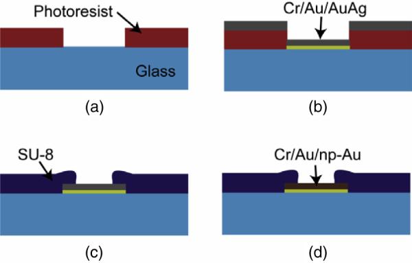
Fabrication of multiple-electrode array: (a) 4 μm thick photoresist is patterned on a glass microscope slide; (b) varying thicknesses and alloy composition of gold–silver is sputter-deposited and consequently lifted off to pattern the electrodes; (c) 2 μm thick SU-8 is patterned to insulate the electrodes except for the ~32 μm diameter circular sensing regions and peripheral electrical contacts; (d) electrodes are dealloyed in nitric acid at 70 °C to produce nanoporous gold electrodes.
2.3. Characterization of electrodes
The AuAg and np-Au film thicknesses were calculated based on previously determined single-layer film deposition rates for the exact conditions used for depositing the actual electrodes. The np-Au film thickness was determined by first measuring the total film thickness over the np-Au contact pad and then subtracting thickness of the non-porous Cr/Au layer underneath. The electrode thickness was measured with a Dektak 8 profilometer using low stylus force of 10 μN. We used a Zeiss FESEM SUPRA 40 scanning electron microscope (SEM) to capture the morphology of different electrodes at 150 000 magnification and determine the elemental composition of deposited and dealloyed electrodes using energy dispersive spectroscopy instrument attached to this SEM.
2.4. Porosity analysis
We used ImageJ (NIH shareware, http://rsb.info.nih.gov/ij/index.html) for np-Au porosity analysis, as described elsewhere [20]. First, the gray-scale images were manually segmented into monochrome images by selecting a threshold gray value that separated `dark' pores and `light' ligaments. We used the built-in `watershed' tool to separate the segmented pores into approximately circular individual pieces. The per cent area covered by the pores and the area of each circular piece were calculated with the built-in `particle analysis' algorithm in ImageJ. We then approximated the total surface area of an electrode as follows: the total volume of the spherical pores within a single circular electrode tip is:
| (1) |
where β is the porosity, h is the film thickness, and R is the radius of the electrode tip. The number of spherical pores that can fill the volume total volume is:
| (2) |
where r is the spherical pore radius, which was calculated from pore area that corresponded to one standard deviation above the mean pore area for normally distributed pore areas. We then used the number of pores to compute the total surface area:
| (3) |
2.5. Impedance measurement
We measured the impedance of np-Au MEAs and control MEAs, by applying a 200 mV amplitude signal between MEA electrodes and an Ag/AgCl counter electrode, in ACSF, at frequencies ranging between 0.5 and 20 kHz. We measured a minimum of five electrodes for each type of np-Au MEAs and for regular compact-Au MEA. To measure impedance as a function of electrode area, we prepared np-Au MEAs without SU-8 insulation. We then cut an opening in a 50 μm thick PDMS film, and aligned the film to the MEA such that a portion of the electrode tip, or the electrode tip as well as a portion of its connecting trace was exposed to ACSF. We determined the exposed area of np-Au with ImageJ analysis of digital micrographs of the electrodes.
2.6. Hippocampal slice preparation
We dissected 350 μm thick hippocampus slices from postnatal day 7 Sprague-Dawley rat pups (Charles River Laboratories) and maintained them as interface-type organotypic cultures in a humidified 5% CO2 incubator at 37 °C. We used serum-containing (1:1:2 horse serum, Hanks' balanced salt solution, and Basal Medium Eagle, supplemented with 1 mM glutamine and 30 μg ml−1 gentamicin, all from Invitrogen) for first 24 h of culture, and then substituted it with serum-free medium (Neurobasal A/B27, with 0.5 mM glutamine and 30 μg ml−1 gentamicin, all from Invitrogen), which was then used in all subsequent medium changes (every 3 days). The experiments were conducted with the guideline and approval of the Massachusetts General Hospital Subcommittee on Research Animal Care.
2.7. Electrophysiology
In order to record field potentials using the np-Au MEA, we used the method recently developed by our group [21]. Briefly, we fabricated a flexible 150 μm thick PDMS film with a 3 mm diameter well to accommodate hippocampus slice cultures. We then placed the film onto a np-Au MEA so that the slice well was centered on the electrode array. We gently removed organotypic slices from culture dishes on 21st day in vitro (DIV), and placed them into the PDMS well on np-Au MEA. We acquired recordings from the hippocampal cultures in ACSF (composition described above) and ACSF with 2.1 mM KCl addition in a humidified 5% CO2, 37 °C incubator. Signals from MEA were amplified, digitized, and filtered with 3 Hz high-pass filter and 55–65 Hz band-stop Butterworth filter (to remove line noise).
3. Results and discussion
In this study, we demonstrated significantly reduced electrode impedance using nanoporous gold as coating material and showed functionality of the fabricated MEA in recording field potentials. The presented approach takes advantage of a nano-scale self-assembly process and microfabrication technology to greatly simplify electrode fabrication with repeatable improvement in impedance for different film thicknesses and morphologies.
3.1. Material analysis
Immersion of AuAg alloy in nitric acid results in surface diffusion of gold and silver atoms, and selective dissolution of silver atoms, which produces a structure with open-pore morphology [18]. The main advantage of this technique is its reproducibility and compatibility with conventional microfabrication techniques, thus enabling its scalability and broadening its applications in microsystems [19, 20]. Elemental analysis of the AuAg alloy films used for producing np-Au electrodes indicated ~76% (at.%) for the Ag+ sample and ~69% (at.%) for all other samples. All dealloyed films contained less than 5% (at.%) residual silver. During dealloying some amount of silver is passivated by surrounding gold atoms and further etching in nitric acid does not reduce the residual silver content, suggesting that silver does not leach from electrodes into the culture or recording medium [18]. Figure 2 illustrates high-magnification scanning electron micrographs of the different MEAs used in the study. Compact-gold control electrode displayed typical granularity of a sputtered film [22]. The porous electrodes exhibited micro-scale voids due to volume shrinkage during dealloying. These voids do not necessarily affect electrode performance, but actually improve film adhesion by mitigating tensile stress accumulation that usually leads to film delamination. We analyzed the micrographs with ImageJ digital imaging software to obtain per cent porosities (ratio of dark area to total image area) and areas of individual pores. 2D porosity of the surface is consistent through the film thickness, as the homogeneous pore morphology in the SEM cross-section suggests (figure 2). We therefore concluded that porosity and area data obtained by analysis of the 2D image can be used to make an estimate of the total surface area. Per cent porosities of the films were 38%, 32%, and 34% for increasing film thickness (standard alloy composition) and 26% (higher initial silver content, denoted as Ag+). The mean pore radii were 20, 41, and 31 nm for increasing film thickness (standard alloy composition) and 22 nm (Ag+). Nanoporous gold film thicknesses were 112, 166, and 304 nm (standard alloy composition) and 161 nm (Ag+). The total surface area generally increased with film thickness. Despite the moderate thickness and lower per cent porosity of the `Ag+' film, its total surface area was comparable to the thickest np-Au film. As seen in equation (3), the total surface area scales with (βh/r); that is, initial silver-rich alloy resulted in smaller pore sizes, which in turn yielded a high total surface area.
Figure 2.
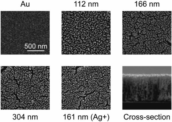
Scanning electron microscope images of MEAs at the same magnification. `Ag+' indicates the sample that had a higher initial silver concentration. Cross-sectional image illustrates the homogeneous pore morphology along the film thickness (a thicker film is intentionally presented to demonstrate consistent homogeneity across a large thickness).
Polymer coatings on metals and semiconductors generally suffer from delamination due to their poor adhesion to dissimilar materials such as metals and semiconductors. Metals of interest such as platinum and gold, when preceded with deposition of adhesive layers such as chrome and titanium, adhere strongly to metals and semiconductors. Nanoporous gold films remained intact throughout our experiments and prolonged immersion (>4 months) in phosphate buffered saline solution (data not shown), whereas most polymers swell in the presence of liquid and delaminate due to mechanical instability [23]. Nanoporous gold coating can alleviate the polymer delamination issue when used as an intermediate adhesive layer between metal/semiconductor and polymer coatings. We have recently demonstrated this technique between np-Au leafs and PDMS that produced highly adherent bilayers through mechanical interlocking of the polymer and the porous network [24]. We expect this technique to enable the integration of desirable conducting polymers, which often could not be used due to delamination problems.
3.2. MEA impedance
Figure 3(a) highlights the >25-fold decrease in impedance of np-Au electrode compared to gold control electrode, as a result of augmented total surface area. This 304 nm thick electrode yields an impedance of ~30 kΩ at 1 kHz, which is three times lower than the typical 100 kΩ impedance of platinum black electrodes [25]. Platinum black electrodes are traditionally produced by platinum electroplating of a rough platinum layer, thus enhancing the effective electrode surface area. Unfortunately, electroplating requires additional fabrication steps and suffers from process-to-process and across-substrate variations. Figure 3(b) provides a comparison of np-Au electrodes with varying thicknesses and initial alloy composition. The electrode impedance generally decreased with increased film thickness for electrodes with the same initial alloy composition, as expected from the relationship, ∝ Asurface ∝ (βh/r), where Z is the electrode impedance. However, as the np-Au film produced by dealloying a silver-rich alloy (Ag+) leads to total surface area comparable to that of the 304 nm thick np-Au electrode, the impedance for the Ag+ electrode is also comparable to that of the 304 nm thick np-Au electrode. Error bars display the standard deviation of measurements from at least five different electrodes on a chip and suggest a high electrode-to-electrode repeatability attained by the developed fabrication method. Additionally, in order to evaluate morphology (consequently the impedance) reproducibility, we performed image analysis on five other samples produced using the same process parameters with that of the 304 nm thick MEA. The five samples were approximately 300 nm thick. The combined average porosity and average pore radius of the five samples and the 304 nm thick MEA were 33.4 ± 1.2% and 29.5 ± 3.8 nm respectively. The impedance of the porous MEAs strongly depends on their morphology and hence the small standard deviations from the six samples fabricated at different times, but with the same process parameters, suggest that the np-Au MEA fabrication process discussed here is highly reproducible. Overall, consistently lower impedance values across different np-Au electrode types evidence the repeatability of the overall impedance improvement. Figure 3(c) demonstrates the relationship between impedance and total electrode surface area and electrode footprint (inset). We fabricated a np-Au chip (identical to the 304 nm thick MEA that displayed the biggest impedance enhancement) without the SU-8 insulation layer in order to systematically vary the electrode area exposed to electrolyte to determine the impedance–area relationship. Our aim was to study the linearity of impedance versus electrode footprint relationship. As seen in figure 3(c) inset, the impedance decreased linearly between 400 and 1100 μm2. In order to evaluate the extent of wetting underneath the PDMS sheet through the pores, we compared two 112 nm thick MEAs, where in one only the electrode tips were porous (as the MEA was dealloyed after SU-8 patterning, therefore preventing pore formation underneath the SU-8 layer) and in the other a fully dealloyed MEA (produced with the same deposition conditions as the former) was covered with PDMS to partially insulate the electrodes. The impedances measured for the same footprint at 1 kHz were 69.5 ± 12.7 kΩ and 77.7 ± 16.5kΩ respectively, which are indistinguishable from each other. This result suggests that the wetting underneath the PDMS sheet does not affect electrode impedance. One possible explanation is the large viscous drag along the length of the porous electrode trace and the small electrode cross-section that channels the bulk ACSF into the electrode. It is also likely that the series resistance of the fluid in the electrode pores underneath PDMS is very high, again due to small electrode cross-section under the passivation layer. The larger series resistance can compensate for the increase in liquid–metal contact area under PDMS, resulting in no net change to electrode impedance. Figure 3(c) displays that electrode impedance decreased with total electrode surface area. The impedance value is a complex combination of the electrode double-layer capacitance, resistance due to leakage through this capacitance, and resistance of patterned metal electrode. An analysis of impedance and its equivalent electrical circuit model is beyond the scope of this paper, and it can be found elsewhere [26].
Figure 3.

Impedance for MEAs with different film thicknesses and initial alloy composition. (a) There is more than 25-fold magnitude improvement in impedance for np-Au electrodes compared to conventional compact-gold electrodes. The curve fits are for visual aid. (b) Impedance, Z, of nanoporous gold MEAs generally decrease with increasing thickness, as total surface area scales with thickness, as shown with the arrow. However, MEA with a higher pre-dealloying silver content creates a structure with higher unit surface area per thickness, thus results in less impedance compared to MEAs with similar thickness. Error bars show the standard deviation from measurements of at least five different electrodes per sample. The curve fits are for visual aid. (c) The electrode impedance (at 1 kHz) is inversely proportional to total surface area of the electrode. Horizontal error bars indicate standard deviations of total surface area, which is calculated using three different scanning electron micrographs and film thickness measurements per sample. The inset illustrates the linear dependence of impedance to electrode footprint. The arrow indicates decreasing impedance with increasing excitation frequency.
3.3. Recording of spontaneous activity in hippocampal cultures
We placed a 21 DIV organotypic hippocampal slice culture onto a np-Au MEA (figure 4(a)), and recorded spontaneous activity. Single- and multiple-unit activity was observed in ACSF (figure 4((b), right)), and epileptiform bursts were recorded in ACSF containing an elevated concentration of K+ (5.4 mM, figure 4(c)). Unit activity in slices is generally hard to detect with planar MEA electrodes. This is due to low amplitude of single units (<100 μV) and the physical separation between planar electrodes and the axon initial segment (region that is thought to be responsible for most of the extracellular signal generated by an action potential). The physical separation is caused by surface layers of dead cells in acute slices, or by a surface layer of glia in organotypic cultures. Low impedance of np-Au electrodes helped reduced noise levels (random noise at the electrode–electrolyte interface as well as contributions from the noisy environment of the incubator where recordings were performed and the length of electrical lines between the incubator and amplifiers) to the point where unit activity could be detected. On the other hand, standard electrodes were significantly noisier, and lower amplitude single units (from neurons located further away from the recording electrode) could not be discerned. Noise Vrms of standard electrodes in our recording setup was 8.3 μV, while noise Vrms of np-Au electrodes was 5.5 μV. This experiment demonstrated the utility of np-Au MEA electrodes in recording neural activity ranging from single units to network-wide bursts.
Figure 4.

(a) Micrograph of hippocampal brain slice over np-Au MEA. The circle indicates the electrode position in the CA3 region where the field potentials in (b), (right) and (c) were recorded. (b) Recordings of multi-unit spontaneous activity of slice in physiological buffer. Left: recording with a standard electrode. Right: recording with a np-Au electrode. (c) Recordings of epileptiform bursts induced by elevated [K+] on np-Au MEA. The scale bar is 200 μm.
4. Conclusions
We presented a simple, scalable, and repeatable technique to produce multiple-electrode arrays with impedance values better than those of state-of-the-art platinum black electrode coatings, by utilizing a combination of nano-scale self-assembly and microfabrication technology. We demonstrated the utility of the nanoporous electrode array in recording unit and burst activity from hippocampal slice cultures. Our current efforts are focused on using the well-defined surface chemistry of gold to improve tissue-electrode interaction.
Acknowledgments
This work was sponsored in part by NIH Grant P41-EB002503, New Jersey Commission on Brain Injury Research Grant 08-3210-BIR-E-1, and NSF Grant DMI-0507023. YB was supported by NIH F32-MH079662.
References
- [1].Rutten WL. Selective electrical interfaces with the nervous system. Annu. Rev. Biomed. Eng. 2002;4:407–52. doi: 10.1146/annurev.bioeng.4.020702.153427. [DOI] [PubMed] [Google Scholar]
- [2].Pearce TM, Williams JC. Microtechnology: meet neurobiology. Lab Chip. 2007;7:30–40. doi: 10.1039/b612856b. [DOI] [PubMed] [Google Scholar]
- [3].Morin FO, Takamura Y, Tamiya E. Investigating neuronal activity with planar microelectrode arrays: achievements and new perspectives. J. Biosci. Bioeng. 2005;100:131–43. doi: 10.1263/jbb.100.131. [DOI] [PubMed] [Google Scholar]
- [4].Gross GW, Williams AN, Lucas JH. Recording of spontaneous activity with photoetched microelectrode surfaces from mouse spinal neurons in culture. J. Neurosci. Methods. 1982;5:13–22. doi: 10.1016/0165-0270(82)90046-2. [DOI] [PubMed] [Google Scholar]
- [5].Pancrazio JJ, et al. A portable microelectrode array recording system incorporating cultured neuronal networks for neurotoxin detection. Biosens. Bioelectron. 2003;18:1339–47. doi: 10.1016/s0956-5663(03)00092-7. [DOI] [PubMed] [Google Scholar]
- [6].Eytan D, Brenner N, Marom S. Selective adaptation in networks of cortical neurons. J. Neurosci. 2003;23:9349–56. doi: 10.1523/JNEUROSCI.23-28-09349.2003. [DOI] [PMC free article] [PubMed] [Google Scholar]
- [7].Morin F, Nishimura N, Griscom L, Lepioufle B, Fujita H, Takamura Y, Tamiya E. Constraining the connectivity of neuronal networks cultured on microelectrode arrays with microfluidic techniques: a step towards neuron-based functional chips. Biosens. Bioelectron. 2006;21:1093–100. doi: 10.1016/j.bios.2005.04.020. [DOI] [PubMed] [Google Scholar]
- [8].Chang JC, Brewer GJ, Wheeler BC. Modulation of neural network activity by patterning. Biosens. Bioelectron. 2001;16:527–33. doi: 10.1016/s0956-5663(01)00166-x. [DOI] [PubMed] [Google Scholar]
- [9].Nam Y, Chang J, Khatami D, Brewer GJ, Wheeler BC. Patterning to enhance activity of cultured neuronal networks. IEE Proc. Nanobiotechnol. 2004;151:109–15. doi: 10.1049/ip-nbt:20040706. [DOI] [PubMed] [Google Scholar]
- [10].Uesaka N, Hayano Y, Yamada A, Yamamoto N. Interplay between laminar specificity and activity-dependent mechanisms of thalamocortical axon branching. J. Neurosci. 2007;27:5215–23. doi: 10.1523/JNEUROSCI.4685-06.2007. [DOI] [PMC free article] [PubMed] [Google Scholar]
- [11].Jones G, Bollinger GM. The measurement of the conductance of electrolytes. VII. On platinization. J. Am. Chem. Soc. 1935;57:280–4. [Google Scholar]
- [12].Geddes LA. Electrodes and the Measurement of Bioelectric Events. Wiley-Interscience; New York: 1972. [Google Scholar]
- [13].Bauerdick S, Burkhardt C, Kern DP, Nisch W. BioMEMS materials and fabrication technology. Biomed. Microdev. 2003;5:93–9. [Google Scholar]
- [14].Moxon KA, Kalkhoran NM, Markert M, Sambito MA, McKenzie JL, Webster JT. Nanostructured surface modification of ceramic-based microelectrodes to enhance biocompatibility for a direct brain–machine interface. IEEE Trans. Biomed. Eng. 2004;51:881–9. doi: 10.1109/TBME.2004.827465. [DOI] [PubMed] [Google Scholar]
- [15].Cui X, Hetke J, Wiler J, Anderson D, Martin D. Electrochemical deposition and characterization of conducting polymer polypyrrole/PSS on multichannel neural probes. Sensors Actuators A. 2001;93:8–18. [Google Scholar]
- [16].Yang J, Martin D. Microporous conducting polymers on neuroal microelectrode arrays II. Physical characterization. Sensors Actuators A. 2004;113:204–11. [Google Scholar]
- [17].Cui X, Martin D. Fuzzy gold electrodes for lowering impedance and improving adhesion with electrodeposited conducting polymer films. Sensors Actuators A. 2003;103:384–94. [Google Scholar]
- [18].Erlebacher J, Aziz M, Karma A, Dimitrov N, Sieradzki K. Evolution of nanoporosity in dealloying. Nature. 2001;410:450–3. doi: 10.1038/35068529. [DOI] [PubMed] [Google Scholar]
- [19].Seker E, Begley M, Reed M, Utz M. Kinetics of capillary wetting in nanoporous films in the presence of surface evaporation. Appl. Phys. Lett. 2008;92:013128. [Google Scholar]
- [20].Seker E, Gaskins J, Bart-Smith H, Zhu J, Reed M, Zangari G, Kelly R, Begley M. The effects of post-fabrication annealing on the mechanical properties of freestanding nanoporous gold structures. Acta Mater. 2007;55:4593–602. [Google Scholar]
- [21].Berdichevsky Y, Sabolek H, Levine J, Staley K, Yarmush M. Microfluidics and multielectrode array-compatible organotypic slice culture method. J. Neurosci. Methods. 2009;178:59–64. doi: 10.1016/j.jneumeth.2008.11.016. [DOI] [PMC free article] [PubMed] [Google Scholar]
- [22].Seker E, Reed M, Begley M. A thermal treatment approach to reduce microscale void formation in blanket nanoporous gold films. Scr. Mater. 2009;60:435–8. [Google Scholar]
- [23].Green R, Lovell N, Wallace G, Poole-Warren L. Conducting polymers for neural interfaces: challenges in developing an effective long-term implant. Biomaterials. 2008;29:3393–9. doi: 10.1016/j.biomaterials.2008.04.047. [DOI] [PubMed] [Google Scholar]
- [24].Seker E, Reed M, Utz M, Begley M. Flexible and conductive bilayer membranes of nanoporous gold and silicone: synthesis and characterization. Appl. Phys. Lett. 2008;92:154101. [Google Scholar]
- [25].Robinson D. The electrical properties of metal microelectrodes. Proc. IEEE. 1968;56:1065–71. [Google Scholar]
- [26].Heer F, Franks W, Blau A, Taschini S, Ziegler C, Hierlemann A, Baltes H. CMOS microelectrode array for the monitoring of electrogenic cells. Biosens. Bioelectron. 2004;20:358–66. doi: 10.1016/j.bios.2004.02.006. [DOI] [PubMed] [Google Scholar]