

Abstract
Detailed understanding of the mechanism of dielectrophoresis (DEP) and the drastic improvement of its efficiency for small size quantized nanoparticles (NPs) open the door for the convergence of microscale and nanoscale technologies. It was hindered however by the severe reduction of DEP force in particles with volume below few hundred nm3. We report here DEP assembly of size quantized CdTe nanoparticles (NPs) with a diameter of 4.2 nm under AC voltage of 4–10 V. Calculations of the nominal DEP force for these NPs indicate that it is several orders of magnitude smaller than the force of the Brownian motion destroying the assemblies even for the maximum applied AC voltage. Despite this theoretical background, very efficient formation of NP bridges between electrodes separated by a gap of 2μ was observed even for AC voltages of 6V and highly dilutes NP dispersions. The resolution of this conundrum was found in the intrinsic ability of CdTe NPs to self-assemble. The species being assembled by DEP are substantially bigger than the individual NPs. DEP assembly should be treated as a process taking place for NP chains with a length of ca 140 nm. The self-assembled chains increase the nominal volume where the polarization of the particles takes place, while retaining the size-quantized nature of the material. The produced NP bridges were found to be photoactive producing photocurrent upon illumination. DEP bridges of quantum confined NPs can be used in fast parallel manufacturing of novel MEMS components, sensors, optical, and optoelectronic devices. Purposeful engineering of self-assembling properties of NPs makes possible further facilitation of the DEP assemblies and increase of complexity of the produced nano- and microscale structures.
The convergence of highly efficient methods of microfabrication and high performance nanomaterials with size-quantized properties holds substantial promise for electronics, photonics, sensors, biological implants, and many other technologies.1 Such convergence will require in many cases that functional elements would be prepared from millions of nanoparticles (NPs) to bridge scales of assemblies from nanometers to micrometers. Assembly of extended patterns from large number of NPs demonstrated for microparticles,2 can potentially be achieved using dielectrophoresis (DEP), i.e. manipulation of particles using non-uniform electric fields.3 Despite observations of DEP for some nanoscale species,6,7,8,9 its mechanism, and its realization for small semiconductor NPs still need to be investigated. The problem here is that the magnitude of DEP force, FDEP, increases with field gradient and the volume of the particle (Supplementary Information, SI).4 Proportionality to the volume greatly exacerbates the dependence of FDEP on the particle diameter, dNP, and thus, DEP typically requires the particles to be relatively large (50nm and above). The gradient of the electrical field over volume of quantum dots is so small that FDEP becomes negligible compared to the force of the Brownian motion, FB. For NPs with dNP=2–5 nm FDEP is 100–5000 times smaller than FB. Consequently, DEP has obvious difficulties when it comes to manipulations of small NPs. Incidentally, the small NPs has the greatest degree of quantum confinement and show unique electronic, optical, and catalytic properties which are yet to be technologically exploited.5 DEP assembly of relatively small NPs was observed only in very narrow gaps and with a small number (below one hundred) of NPs.6,7 Utilization of highly polarizable metallic NPs of Au and Pd increases FDEP and improves the efficiency of DEP assembly,8,9,15 but the challenges with both understanding the reasons behind DEP of small NPs, and its realization for fast production of NP-based components still remain. Besides the academic importance of realization of DEP for quantum-sized NPs, the practical connotations of this work include manufacturing of energy conversion devices (solar cells), a new type of suspended MEMS elements, environmental sensors, and submicron pixels for flexible LED display. All these technologies need to combine spacial X-Y determinism in micron/submicron scales, tunable electrical/electrooptical properties, and fast massive NP assembly process which is difficult to achieve by other colloidal deposition techniques such as ink-jet, spin coating, and microcontact printing.17,18,19
Taking CdTe NPs as a convenient model, we show in this communication that even small semiconductor NPs for which DEP force is supposed to be miniscule, can still be assembled by DEP. Experiments and calculations demonstrate that the native tendency of CdTe NP to self-organize spontaneously in solution into chains without applied electrical field enable the subsequent DEP assembly and provide opportunities for further improvements.
CdTe is one of the most important semiconductor materials with many attractive electronic properties in the size-quantized state including high charge carrier mobility. CdTe NPs stabilized by thioglycolic acid were synthesized (see Supplementary Information, SI) according to Ref.10 in a form of aqueous dispersions with a concentration of 18 μmol/L. The average NP diameter based on the luminescence peak was 2.9 nm (SI). Diameter of these NPs determined from the TEM data was dNP =4.2±1.1 nm and was likely to be an overestimate. Better TEM contrast characteristic for larger NPs causes a shift of statistical curves toward larger sizes. Considering size distribution, we also want to note that not all the NPs could potentially participate in DEP assembly. The larger NPs from the ensemble are associated with greater DEP force and may, in principle, be the sole contributors to the assembly. Therefore, one needs to take into account both the average size and a fraction of larger NPs present in dispersion.
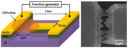
The NPs displayed expectedly strong luminescence (λ =557 nm), high monodispersity, and crystallinity (SI). DEP electrodes separated by a 2 μm gap were formed on a thermally oxidized Si wafer (Figure 1, S3) by traditional lithography. The electrodes were designed to be asymmetric with a difference in width of 1:100 (Figure 1a) in order to increase non-uniformity of the electrical field. 50 μL droplet of diluted CdTe NPs with a concentration of 1.8 μmol/L was placed over the electrodes (Figure 1c) and then the AC voltage of different frequencies (ω) and magnitudes (Vpp) was applied (Figure 2b,c,d). As indicated by the sequence of FESEM images in Figure 2, the first DEP assemblies of CdTe NPs were observed at a peak-to-peak AC voltage, Vpp, of 6V. As Vpp increased, the 2μm gap between the electrodes was successfully bridged (Figure 2b,c,d). A conservative estimate of the total number of NPs drawn by DEP into the microscale electrode gap is 1.4 million (SI) in each bridge. Note that DEP assembly in our case was very efficient; we had to reduce the concentration of as-synthesized NP dispersion as much as 10 times to observe intermediate stages of the assembly. When the concentration of NPs solution was further decreased to 0.36 μmol/L, CdTe nanobridges were also formed under the same conditions although at lower volumetric density (SI).
Figure 1.

(a,b) FESEM image of DEP electrodes. (b) Enlarged view of the area marked by the dotted white circle in (a). Due to the undercut caused by wet etching of the Au layer, the edge of underlying Cr layer was exposed. (c) Schematic diagram of experimental setup for DEP. (d) TEM image of the 50 μL CdTe NPs dispersion after DEP.
Figure 2.

FESEM images after DEP of 1.8 μmol/L NPs solution with Vpp equal to (a) 4, (b) 6, (c) 8, and (d) 10 V. (e,f) Low- and high-magnification FESEM images after DEP of 0.36 μmol/L NPs solution with Vpp=10 V using. (g) fluorescent microscopy images of the electrodes before and after the electrophoretic deposition of NPs (excitation light 360 nm). The frequency and duration of AC voltage were 100 kHz and 30 min, respectively.
Energy-dispersive X-ray (EDX) spectroscopy confirmed that the material deposited between the electrodes is indeed CdTe (Figure 3a). Another well-known property of CdTe, such as photoconductivity was also observed for the DEP-assembled NPs. The current–voltage (I–V) curves of the CdTe microscale bridges (Figure 2d) measured with and without 1.35 mW/cm2 UV irradiation. Largely symmetrical non-linear I–V curve under UV irradiation implies that the Schottky barriers at the junctions between semiconducting CdTe bridges and metal electrodes are fairly identical13 as expected for this device. The observation of photoconductivity provides an additional piece of evidence that not only elemental composition but also the functional properties of the parent semiconductor material were retained in the DEP assemblies of CdTe NPs. This fact also opened the possibility for the fluorescent microscopy imaging (Fig. 2g, h). Strong green luminescence of the deposits between the electrodes (Figure 2h) indicated that the NPs indeed possessed quantum confinement properties.
Figure 3.

(a) EDX elemental analysis of CdTe nanobridges in Figure 2d. (b) I–V characteristics of the CdTe nanobridges measured with and without UV irradiation intensity of 1.35 mW/cm2.
Unexpectedly high efficiency of DEP in our experiments prompted us to look into the reasons behind it. Let us assume the assembly of NPs can occur if the DEP force, FDEP becomes equal or greater that the Brownian motion force, FB. Using the standard equations for both forces (SI) and maximum applied voltage of Vpp=10V, we can see that FDEP is at least three orders of magnitude smaller than FB (SI) even for the fraction of larger NPs with dNP =4.2 nm obtained from TEM. The same remains certainly true when the calculations of FDEP and FB are carried out for the average NP size dNP =2.9 nm obtained from the luminescence data. The observed results are difficult to rationalize in the framework of standard DEP approach but the can be explained if we hypothesize that the actual species that undergo DEP assembly in case of CdTe and potentially many other cases of NPs are actually agglomerates self-assembled in solution following a specific pattern. As such, NP chains are known to spontaneously form for CdTe NP in solution at room temperature.14,20 If this is correct, the equation FDEP = FB can help us determine the diameter of the NPs undergoing DEP assembly. Since the onset of DEP is observed at Vpp=6V, we can calculate that the actual diameter of the particles participating in DEP is 140 nm. TEM taken after DEP assembly showed that there are indeed many chains of NPs formed in the solution with the length of 80–150 nm. These chains are likely to be the actual “particles” being assembled by DEP in case of CdTe dispersion. Analogous sizes of spontaneously assembled species were obtained by dynamic light scattering (DLS). The average DLS particle size was 125 nm which coincided very well with both the calculations (SI) and TEM data. Note that the particle chains may or may not be electrically conductive for DEP to occur as long as their length results in a sufficient gradient of electrical field at each end.2–5 The conductivity of the chains is likely to change as DEP occurs since both expulsion of stabilizer and recrystallization of CdTe can occur.14,20 The resulting assemblies have distinct conductivity benefiting from the direct contact of NP cores and substantial reduction of stabilizer density on NP surface, which is significant considering potential applications of such assemblies for MEMS, electrical, and optoelectronic devices.
In conclusion, we have demonstrated a versatile and facile DEP assembly of semiconductor microscale bridges from fluorescent size quantized CdTe NPs (Fig. 2h). Intrinsic self-organization of CdTe NPs in chains enables DEP despite their minute volume. The observed chains increase the nominal volume where the DEP polarization of the particles takes place, while retaining the size-quantized nature of the material being assembled. In fact all self-assembly processes between NPs including those producing sheets,20 helices,21 and other structures will facilitate their DEP. Stochastic agglomeration, at the same time, will increase FDEP, but is difficult to control and is likely to produce precipitates dominating over formation of DEP bridges.
Further studies might include detailed investigation of DEP in respect to the frequency of applied field (ω) (SI),12 which will help with more detailed evaluation of the Clausius-Mosotti factor (CM), the role of electroosmotic flow in DEP,11,15 and the nature of conductivity NP chains in solution important for potential optoelectronic applications. Assembly behavior might also explain some anomalous behavior of NPs in DEP.16 Purposeful engineering of anisotropic attraction between NPs also provides a method to increase the complexity of produced patterns.
From the application standpoint, integration of electronic elements from small NPs with microscale chips produced by inexpensive standard photolithography greatly facilitates appearance of realistic incarnations of these devices scalable to the needs of electronic industry.
Supplementary Material
Acknowledgments
This material is based upon work partially supported by the Center for Solar and Thermal Energy Conversion, an Energy Frontier Research Center funded by the U.S. Department of Energy, Office of Science, Office of Basic Energy Sciences under Award Number #DE-SC0000957. We acknowledge support from NSF under grant ECS-0601345; EFRI-BSBA 0938019; CBET 0933384; CBET 0932823; and CBET 1036672. The work is also partially supported by AFOSR MURI 444286-P061716 and NIH 1R21CA121841-01A2. The authors thank the University of Michigan’s EMAL for its assistance with electron microscopy, and for the NSF grant #DMR-9871177 for funding for the JEOL 2010F analytical electron microscope used in this work.
Footnotes
Supporting Information Available: Experimental details; UV-Vis/PL spectra, HRTEM, concentration calculation of NPs.
References
- 1.Krupke R, Hennrich F, Weber HB, Kappes MM, Löhneysen Hv. Nano Letters. 2003;3(8):1019–1023. [Google Scholar]
- 2.Lumsdon SO, Kaler EW, Williams JP, Velev OD. Appl Phys Lett. 82(6):949–951. [Google Scholar]
- 3.Riegelman M, Liu H, Bau HH. J Fluid Eng-T ASME. 2006;128:6–13. [Google Scholar]
- 4.Lapizco-Encinas BH, Rito-Palomares M. Electrophoresis. 2007;28:4521–4538. doi: 10.1002/elps.200700303. [DOI] [PubMed] [Google Scholar]
- 5.Pohl HA. Dielectrophoresis. Cambridge University Press; Cambridge: 1978. [Google Scholar]
- 6.Barsotti RJ, Jr, Vahey MD, Wartena R, Chiang Y-M, Voldman J, Stellacci F. Small. 2007;3:488–499. doi: 10.1002/smll.200600334. [DOI] [PubMed] [Google Scholar]
- 7.Seo Y-K, Kumar S, Kim G-H. Physica E. 2010;42:1163–1166. [Google Scholar]
- 8.Ranjan N, Vinzelberg H, Mertig M. Small. 2006;2:1490–1496. doi: 10.1002/smll.200600350. [DOI] [PubMed] [Google Scholar]
- 9.Xiong X, Busnaina A, Selvapraba S, Somu S, Wei M, Mead J, Chen C-L, Aceros J, Makaram P, Dokmeci MR. Appl Phys Lett. 2007;91:063101. [Google Scholar]
- 10.Gaponik N, Talapin DV, Rogach AL, Hoppe K, Shevchenko EV, Kornowski A, Eychmüller A, Weller H. J Phys Chem B. 2002;106:7177–7185. [Google Scholar]
- 11.Cheng C, Gonela RK, Gu Q, Haynie DT. Nano Lett. 2005;5:175–178. doi: 10.1021/nl048240q. [DOI] [PubMed] [Google Scholar]
- 12.Ranjan N, Mertig M, Cuniberti G, Pompe W. Langmuir. 2010;26:552–559. doi: 10.1021/la902026e. [DOI] [PubMed] [Google Scholar]
- 13.Kum MC, Yoo BY, Rheem YW, Bozhilov KN, Chen W, Mulchandani A, Myung NV. Nanotechnology. 2008;19:325711. doi: 10.1088/0957-4484/19/32/325711. [DOI] [PubMed] [Google Scholar]
- 14.Tang Z, Kotov NA, Giersig M. Science. 2002;297(5579):237–240. doi: 10.1126/science.1072086. [DOI] [PubMed] [Google Scholar]
- 15.Gierhart BC, Howitt DG, Chen SJ, Smith RL, Collins SD. Langmuir. 2007;23:12450–12456. doi: 10.1021/la701472y. [DOI] [PubMed] [Google Scholar]
- 16.Froude V, Godfroy J, Wang S, Dombek H, Zhu Y. J Phys Chem C. 2010;114(44):18880–1888. [Google Scholar]
- 17.Andres CM, Kotov NA. JACS. 2010;132(41):14496–14502. doi: 10.1021/ja104735a. [DOI] [PMC free article] [PubMed] [Google Scholar]
- 18.Guyot-Sionnest P. Microchim Acta. 2008;160(3):309–314. [Google Scholar]; Sato H, Homma T. J Nanosci Nanotech. 2007;7(1):225–231. [PubMed] [Google Scholar]; Won J, Jegal J, Kang YS. Comptes Rendus Chimie. 2003;6(8–10):1185–1192. [Google Scholar]
- 19.Tsu R. Nanotechnology. 2001;12(4):625–628. [Google Scholar]
- 20.Tang ZY, Zhang ZL, Wang YW, Glotzer S, Kotov NA. Science. 2006;314(5797):274–278. doi: 10.1126/science.1128045. [DOI] [PubMed] [Google Scholar]
- 21.Srivastava S, et al. Science. 2010;327:1355, 1355–1359. doi: 10.1126/science.1177218. [DOI] [PubMed] [Google Scholar]
Associated Data
This section collects any data citations, data availability statements, or supplementary materials included in this article.