Abstract
Due to the very small size of the mouse inner ear, 600 nL volume, developing effective, controlled infusion systems is quite challenging. Key technologies have been created to minimize both size and power for an implantable pump for murine intracochlear infusions. A method for coupling fine capillary tubing to microfluidic channels is presented which provides low volume, biocompatible interconnects withstanding pressures as high as 827 kPa (120 psi) and consuming less than 20 nL of volume exiting in-plane with the pump. Surface micromachined resistive bridges integrated into the flow channel for anemometry based flow rate measurement have been optimized for low power operation in the ultra-low flow rate regime. A process for creation of deformable diaphragms over pump chambers with simultaneous coating of the microfluidic channels has been developed allowing integration of a biocompatible fluid flow path. These advances represent enabling capabilities for a drug delivery system suitable for space constrained applications such as subcutaneous implantation in mice.
Index Terms: Hot-film anemometer, implantable systems, microsystems technologies, microfluidic interconnections
I. Introduction
Advanced hearing loss and deafness therapies that improve auditory function will require carefully timed and dosed, site-directed delivery of multiple therapeutic compounds over a period of time. Syringe and osmotic pumps have proven effective for baseline lab investigations in animal models [1], but lack the flexibility required for more sophisticated therapy development. Needs for this application diverge from those commonly pursued in MEMS based micropumps; specifically accurate delivery of therapeutic agents at nL/min flow rates, a non-reactive, non-water absorbing, biocompatible flow path, and system form factor consistent with subcutaneous implantation in mice. To address these unique requirements, several key integration technologies have been developed: in-plane fluidic interconnects, anemometers optimized for sensitivity and power in the low flow rate regime, and in-situ parylene pump diaphragm formation over parylene coated fluidic microchambers and channels. Fig. 1 is a conceptual drawing of an implantable system incorporating these three technologies.
Fig. 1.
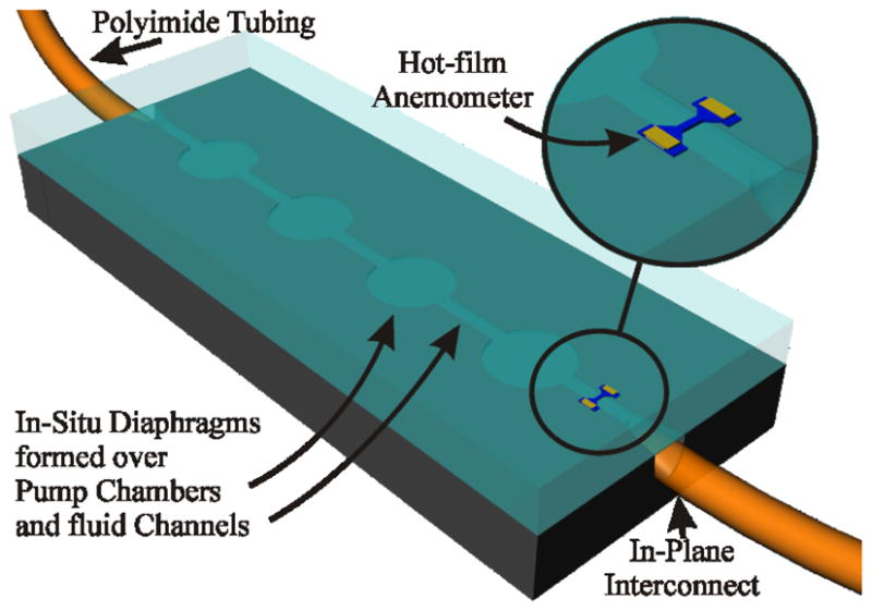
Four chamber peristaltic pump concept with anemometer coupled to 140 μm O.D. capillary tubing. Chambers: 400 μm in diameter, channel width: 100 μm. Overall finished device dimensions anticipated to be 5 mm × 2 mm × 1mm including actuation and RF power coupling (not shown).
Parylene-C (chlorinated poly-para-xylylene) is an attractive material for fluidic systems due to its biocompatibility and chemical resistance [2]. Polyimide tubing, USP Class VI compliant, has been used for biomedical implants as medical probes [3], and micro-channels [4] and is well suited for use as cannulae [5].
II. In-Plane Interconnects
In-plane interfaces to microfluidic systems offer the potential to significantly reduce overall fluidic interconnect volume and the effective device thickness for medical implant applications. Here we present a robust interconnect technology requiring only a single mask level and deposition of Parylene-C onto room temperature surfaces. The long mean-free path of Parylene-C allows narrow gap penetration during deposition [6]; a characteristic which is leveraged to design tapered channels optimized to fill with parylene around an inserted capillary tube.
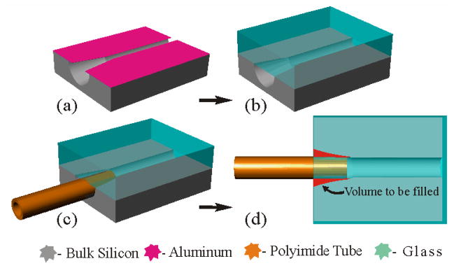
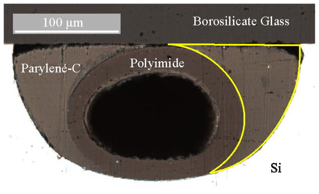
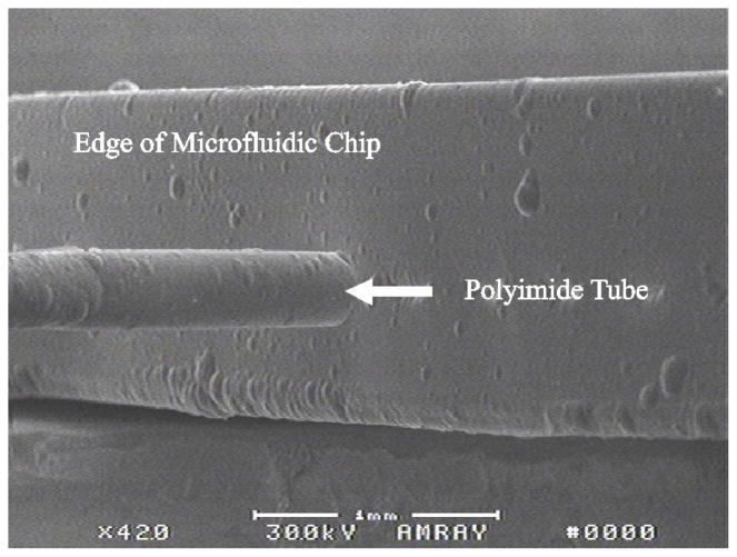
As illustrated in Fig. 2, polyimide capillary tubing (140 μm O.D, Microlumen, Tampa, FL) was inserted in-plane until the tubing end interfaced with the channel walls. Using a modification of the parylene deposition characteristics of Broer and Luijks [7], the channel shape was designed such that the narrow region at the tip of the inserted tubing would occlude first during deposition to provide a fluidic seal and reduce the potential for dead volumes. A 40 μm layer of Parylene-C was deposited to capture the tubing, create a fluidic seal, and fully encapsulate the device to provide a biocompatible surface suitable for medical implantation. The total added volume of the interconnect is 0.018 mm3(18 nL). The devices were pressure tested by connection to compressed argon, submersion in water, and viewing through a microscope to detect air bubbles. No leakage was observed up to the maximum available pressure of 120 psi (N=8). This is higher than the values typically reported in the literature (average ~60 psi) [8–10]. The eight interconnects were then subjected to a pull test with an average force of 2.9 N (σ = 0.6 N, max. = 4.1 N, min. = 2.3 N) required to pull the tubing out of the interconnect channel; a force comparable to the 2–3 N typically reported in the literature for devices using small diameter capillary tubing [8–10]. The eight devices were cross sectioned and imaged under a microscope, as shown in Fig. 3. A scanning electron micrograph of the completed interconnect is shown in Fig. 4 which illustrates the low added volume aspect of this technique.
Fig. 2.
In-plane fluidic interconnect concept and fabrication process. (a) An isotropic Si etch; 100 μm wide microchannels; aluminum mask. (b) Al removed, devices diced and cleaned, borosilicate glass anodically bonded to create the enclosed channels. (c) 140 μm O.D. tubing inserted 500 μm into tapered channel end, 250 μm wide at opening. (d) Top view showing volume to be filled with Parylene in red. Not drawn to scale.
Fig. 3.
Image of cross section of Parylene-C in channel around polyimide tubing. Original designed gap outlined in yellow which has been filled with Parylene-C. Cross section at 50 μm into channel from edge of chip.
Fig. 4.
SEM of the side of the microfluidic chip with small diameter (140 μm O.D.) tubing exiting in-plane.
III. Flow sensing micro-bridges
Suspended microbridges have been designed and fabricated that are able to integrate a flow sensor into the micropump. The flow sensor is a thermal anemometer, in which a resistive element generates heat that is transferred to the fluid. The rate of heat transfer is monitored by a constant-temperature control circuit, and can be correlated to the flow rate. In order to attain the sensitivity required for flow rates on the order of nanoliters per minute, the anemometer is suspended in the middle of the fluid channel, allowing fluid to flow both above and below it. This adds complexity and fragility to the design, but the required sensitivity may not be met if the anemometer is only released from the substrate for thermal isolation [11–12].
The fabrication process is described in Fig. 5, and features a boron-doped polysilicon heater encapsulated by an inner layer of silicon oxide and an outer layer of silicon nitride. The bridge is built on a <100> silicon wafer with a sacrificial polysilicon layer, so that upon KOH etching, the bridge is left suspended over the anisotropically etched microchannel. Minor process modifications will allow the bridge to be fabricated over an isotropically etched channel, compatible with other devices presented. Microchannel sealing with a complementarily etched glass wafer positions the bridge in the middle of the fluid channel.
Fig. 5.
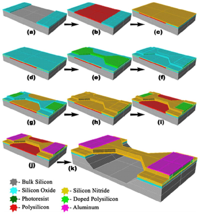
Fabrication process for suspended micro-bridges. (a) 1 μm SiO2 patterned; (b) 1 μm of sacrificial polysilicon patterned; (c) 150 nm of Si3N4 and (d) 50 nm of SiO2 deposited; (e) 600 nm of polysilicon deposited, doped, and patterned to form heating resistors; (f) 50 nm of SiO2 deposited; (g) etched in hydrofluoric acid; (h) 150 nm Si3N4 is deposited; (i) heater bridges patterned by phosphoric acid etching; (j) aluminium deposited and patterned; (k) potassium hydroxide etches the sacrificial polysilicon and bulk silicon.
The primary tradeoff in the anemometer design is power efficiency at the expense of durability. The most efficient anemometer will be as narrow as possible, with the narrow region extending all the way across the fluid channel. The high length-to-width ratio improves the thermal conductance to the fluid, Gfluid, and thus sensitivity. The heat lost to the substrate and thus, wasted power, decreases with bridge width. This ideal sensor is also the most fragile, and with process variation introduced, fabrication may not reliably produce functioning sensors.
To improve the durability of sensors during fabrication, the entire bridge can be made wider, or tapered attachments can connect the narrow heating region to the channel wall. Both of these methods will increase the thermal conductance to the substrate, so heat generated will sink to the substrate of the wafer, instead of being transferred to the fluid. An analysis of relative thermal conductances to the substrate and fluid was used to optimize anemometer design.
Calculation of the thermal conductance to the substrate is straightforward since the geometry is simple and involves solid materials. Determining the thermal conductance to the fluid is considerably more complex, since the heat will diffuse from the rectangular heating area to the surrounding fluid, and will be dependent on the fluid velocity, which follows a complicated profile with the sensor introduced into the channel. King’s law is typically used to calibrate anemometers based on their convection coefficient versus average fluid velocity, u [13], but can also be applied to the thermal conductance, as in (1).
| (1) |
In (1), Gfluid0 is the thermal conductance at zero fluid velocity, and β and χ are fitting parameters. The King’s law fitting parameters for hot-wire anemometers have been thoroughly investigated [13] and can be used to predict the behavior of similar wires. When the shape of a hot-film sensor deviates from a wire, and the size of the sensor is comparable to the size of the fluid channel, the behavior may differ considerably based on the sensor shape.
Finite-element analysis software that will simulate heat transfer from a solid rectangle to moving fluid is being used to develop an explicit form of King’s law for different sensor areas, A, and length-to-width ratios, ζ, in channels of various widths, CW. The fitting parameters in (1), will become functions of the system geometries, as in (2).
| (2) |
It is the relative sensitivity of Gfluid to fluid velocity that will identify an efficient sensor, as excessive heat dissipated to the fluid also constitutes wasted power. The relative thermal sensitivity is expressed in (3).
| (3) |
The values of β, χ, and Gfluid0 determined from finite-element analysis, combined with the thermal conductance to the substrate, reveal how much sensitivity is sacrificed when tapered attachments are introduced, or when the bridge is made wider, to ensure that bridges will tolerate the fabrication process and survive the lifetime of the micropump. The King’s law trend derived from results of thorough finite-element analysis, as in (2), may be used to determine the ideal anemometer shape to meet power requirements and durability constraints.
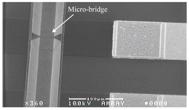
A successful fabrication of a narrow sensor with tapered attachments to the channel wall is shown in Fig. 6. Further process characterization may identify durability limitations, which can then drive the usage of an explicit King’s law expression to determine the ideal anemometer shape for greatest sensitivity versus power consumption.
Fig. 6.
SEM image of a micro-bridge over a KOH-etched channel with tapered attachments to the channel wall. In the narrowest region, the doped polysilicon is 2 μm wide and the silicon nitride is designed to be 8 μm wide. Wide doped polysilicon regions, covered with oxide and nitride can be seen connecting the bridge to aluminum traces.
IV. In-Situ Diaphragm Formation
A process for the creation of deformable diaphragms over pump chambers and channels with simultaneous coating of channel surfaces has been developed allowing integration of a biocompatible fluid flow path.
Parylene diaphragms for pumps or valves can be formed by etching through the back side of a Si wafer [14], sacrificial layer release [15], or by wafer level transfer [16]. Recently, diaphragms for sensors have been formed in-situ by etching-through openings in a Parylene mask with XeF2 [17]. The work presented here is a variant of that process designed to allow thinner diaphragms for this application.
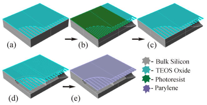
A hard mask of low tensile stress TEOS oxide defines fluidic cavities and acts as a framework onto which Parylene-C is deposited creating a deformable diaphragm. The TEOS is patterned with line/space pairs to define the fluidic regions etched into the surface of the silicon. The small openings (2 μm to 4 μm wide) in the TEOS mask allow for an isotropic Si etch to form the underlying fluidic cavities and is used as a form upon which a coating of Parylene-C is deposited.
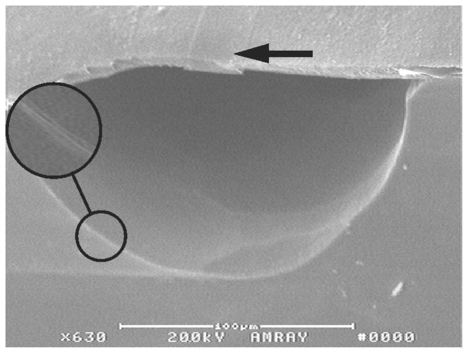
Photo resist was used to protect the chambers and fluid channels during a deep XeF2 etch of the Si to create the interconnects. The photo resist was removed and a shallow etch created the chambers and fluid channels. Fig. 7 is an illustrative diagram of the fabrication showing the technique described. Fig. 8 is a SEM image of a cross sectioned device showing a deep etched fluidic channel under the in-situ formed diaphragm. Diaphragms over pump chambers were successfully created and deflected. The Parylene-C not only forms the diaphragm but also seals the entire microfluidic structure with a biocompatible coating. Fig. 8 shows that the channel has been coated with Parylene-C; further investigation will be needed to quantify the thickness.
Fig. 7.
Fabrication process for in-situ diaphragm formation. (a) SiO2 patterned (b) Deep Isotropic Si etch (c) Photo resist removed (d) Shallow Si etch (e) diaphragm formed, 500 μm diameter, 15 μm deep.
Fig. 8.
SEM image shows deep etched channel under diaphragm. 25 μm stripe (arrow) is a row of openings in the TEOS, filled with Parylene-C. The enlarged area shows the layer of Parylene-C coating the fluid channel.
V. Conclusion
In-plane biocompatible microfluidic interconnects have been characterized, flow sensing micro-bridges have been fabricated, and in-situ fabricated diaphragms have been formed and pneumatically actuated. These technologies will enable the creation of a drug delivery platform suitable for subcutaneous implantation in mice. Future work will include the characterization of the TEOS/PCPX diaphragms. This system will provide capabilities critical for the development of inner ear therapies that address the biological basis of auditory dysfunction.
Acknowledgments
The authors wish to thank the faculty and staff of the RIT Semiconductor and Microsystems Fabrication Laboratory.
This work was supported by the National Institutes of Health, NIDCD (1K25DC008291, P30 DC05409) and NIA (P01 AG09524)
Contributor Information
D. G. Johnson, Email: dgj2607@rit.edu, Rochester Institute of Technology, Rochester, NY 14623 USA.
M. J. Waldron, Email: mjw7675@rit.edu, Rochester Institute of Technology, Rochester, NY 14623 USA.
R. D. Frisina, Email: Robert_Frisina@urmc.rochester.edu, University of Rochester School of Medicine and Dentistry, Rochester, NY 14642 USA
D. A. Borkholder, Email: david.borkholder@rit.edu, Rochester Institute of Technology, Rochester, NY 14623 USA (585-475-6067).
References
- 1.Sefton MV. Implantable Pumps. Critical Reviews in Biomedical Engineering. 1987;14:201–240. [PubMed] [Google Scholar]
- 2.Licari JJ. Coating Materials for Electronic Applications - Polymers, Processes, Reliability, Testing. Vol. 158. William Andrew Publishing/Noyes; 2003. [Google Scholar]
- 3.Metz S, Bertzch A, Bertrand D, Renaud P. Flexible polyimide probes with microelectrodes and embedded microfluidic channels for simultaneous drug delivery and multichannel monitoring of bioelectric activity. Biosensors & Bioelectronics. 2004;19:1309–18. doi: 10.1016/j.bios.2003.11.021. [DOI] [PubMed] [Google Scholar]
- 4.Lacour SP, Atta R, FitzGerald JJ, Blamire M, Tarte E, Fawcett J. Polyimide micro-channel arrays for peripheral nerve regenerative implants. Sensors and Actuators, A: Physical. 2008;147:456–463. [Google Scholar]
- 5.Johnson DG, Zhu XX, Frisina RD, Borkholder DA. Micro-Molded Cannulae for Intracochlear Infusions in Small Rodents. Engineering in Medicine and Biology Society; EMBS 2007. 29th Annual International Conference of the IEEE; 2007; 2007. pp. 6616–6619. [DOI] [PubMed] [Google Scholar]
- 6.Parylene Engineering. Microfluidic Edge Connector. 2020 March 30; Available: http://www.paryleneengineering.com/parylene_deposition_process.html.
- 7.Broer DJ, Luijks W. Penetration Of P-Xylylene Vapor Into Small Channels Prior To Polymerization. Journal of Applied Polymer Science. 1981;26:2415–2422. [Google Scholar]
- 8.Gray BL, et al. Novel interconnection technologies for integrated microfluidic systems. Sensors and Actuators A (Physical) 1999;A77:57–65. [Google Scholar]
- 9.Shifeng L, Shaochen C. Polydimethylsioxane fluidic interconnects for microfluidic systems. IEEE Transactions on Advanced Packaging. 2003;26:242–7. [Google Scholar]
- 10.Tingrui P, Baldi A, Ziaie B. A reworkable adhesive-free interconnection technology for microfluidic systems. Journal of Microelectromechanical Systems. 2006;15:267–72. [Google Scholar]
- 11.Baltes H, Paul O, Brand O. Micromachined thermally based CMOS microsensors. Proceedings of the IEEE. 1998 Aug;86(8):1660–1678. [Google Scholar]
- 12.Fang YJ, et al. Commercialized CMOS Compatible Micro Anemometer. Sensors; 5th IEEE Conference; 22–25 Oct. 2006.2006. pp. 1452–1455. [Google Scholar]
- 13.Lomas CG. Fundamentals of Hot Wire Anemometry. Cambridge University Press; 1986. [Google Scholar]
- 14.Meng E, Xuan-Qi W, Mak H, Yu-Chong T. A check-valved silicone diaphragm pump. Proceedings IEEE Thirteenth Annual International Conference on Micro Electro Mechanical Systems; 23–27 Jan. 2000; Piscataway, NJ, USA. 2000. pp. 62–7. [Google Scholar]
- 15.Majumdar A, Satyanarayana S, McCormick DT. Parylene micro membrane capacitive sensor array for chemical and biological sensing. 2006;115:494–502. [Google Scholar]
- 16.Kim H, Najafi K. Characterization of aligned wafer-level transfer of thin and flexible parylene membranes. 2007;16:1386–1396. [Google Scholar]
- 17.Giacchino L, Yu-Chong T. Parylene-membrane piezoresistive pressure sensors with XeF2-etched cavity. 2008 IEEE Sensors; 26–29 Oct. 2008; Piscataway, NJ, USA. 2008. pp. 1568–71. [Google Scholar]


