

Abstract
Nanowire FETs (NWFETs) are promising building blocks for nanoscale bioelectronic interfaces with cells and tissue since they are known to exhibit exquisite sensitivity in the context of chemical and biological detection, and have the potential to form strongly coupled interfaces with cell membranes. We present a general scheme that can be used to assemble NWs with rationally designed composition and geometry on either planar inorganic or biocompatible flexible plastic surfaces. We demonstrate that these devices can be used to measure signals from neurons, cardiomyocytes, and heart tissue. Reported signals are in millivolts range, which are equal to or substantially greater than those recorded with either planar FETs or multielectrode arrays, and demonstrate one unique advantage of NW-based devices. Basic studies showing the effect of device sensitivity and cell/substrate junction quality on signal magnitude are presented. Finally, our demonstrated ability to design high-density arrays of NWFETs enables us to map signal at the subcellular level, a functionality not enabled by conventional microfabricated devices. These advances could have broad applications in high-throughput drug assays, fundamental biophysical studies of cellular function, and development of powerful prosthetics.
Keywords: Cancer markers, cardiomyocyte, heart, nanowire (NW) transistor, neuron, silicon, virus
I. Introduction
Recording electrical signals from cells and tissue is central to areas ranging from the fundamental biophysical studies of function in, for example, the heart and brain, through medical monitoring and intervention. Over the past several decades, studies of electroactive cells and tissue have been carried out by using a variety of recording techniques, including glass micropipette intracellular (IC) and patch-clamp electrodes [1]–[4], voltage-sensitive dyes [5]–[7], multielectrode arrays (MEAs) [8]–[11], and planar FETs [12]–[19]. The latter two recording techniques use well-developed microfabrication methods to allow for multiplexed detection on a scale not possible with micropipette technology, although the MEAs exhibit limited SNRs and detection areas that make cellular and subcellular recording challenging [20], [21].
A new class of molecular-scale electronic interfaces can be formed with cells and tissue using chemically synthesized semiconductor nanowires (NWs) as functional elements. These NWs have received intense interest in recent years, leading to the development of structures with rationally controlled geometry, composition, and electronic properties [22]–[26]. These characteristics—i.e., rational control of structure, composition, and electronic properties during synthesis—have enabled semiconductor NWs to emerge as powerful building blocks for the bottom-up assembly of functional devices with applications in nanoelectronics, [27]–[32], photonics [24], [33], energy conversion [29], [30], and the biosciences [34]–[36].
A. Nanowires as Biological Sensors
Underlying biological detection using semiconductor NWs [34]–[36] is their configuration as FETs, which exhibit a conductance change in response to variations in the charge or potential at the surface of the channel region, as shown schematically in Fig. 1(a) [37]. This property makes FETs natural candidates for electrically based sensing since binding of a charged or polar biological or chemical species to the gate dielectric is analogous to the conventional case of applying a voltage gate using a metallic gate electrode [see Fig. 1(b)]. Significantly, NWFETs are expected to be more sensitive sensors than their planar counterparts because of their 1-D nanoscale morphology, i.e., an analyte binding to the surface of an NW leads to depletion or accumulation of carriers in the “bulk” of the 1-D nanometer-diameter structure, versus only a shallow region near the surface in the case of a planar device. This unique feature of semiconductor NWs enables exquisite charge sensitivity that opens up new opportunities for interfaces with chemical and biological systems.
Fig. 1.
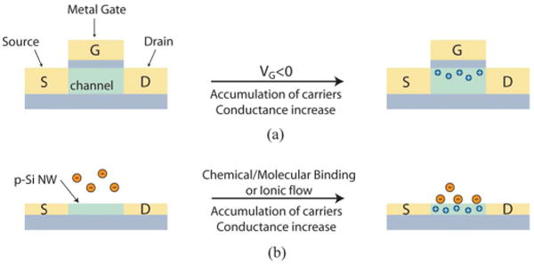
(a) Schematic of a p-type planar FET device, where S, D, and G correspond to source, drain and gate electrodes, respectively. (b) Schematic of electrically based sensing using a p-type NWFET, where binding of a charged biological or chemical species to the chemically modified gate dielectric is analogous to applying a voltage using a gate electrode.
NWs elaborated as well-defined n- or p-channel FETs have, in fact, been used as ultrasensitive sensors of chemical and biological species. This detection capability was first demonstrated in 2001, when measurements in aqueous solution revealed pH sensing as well as selective, label-free detection of proteins and calcium ions [34]. Notably, this NW-based detection technique demonstrated superb sensitivity; for example, biotin-modified NWs were able to detect streptavidin binding down to 10 pM, a sensitivity limit that rivals previously published studies involving single-molecule stochastic binding [38].
In 2004, we achieved the limit of biological detection—single particle sensitivity—by detecting, in real time, the reversible and selective binding of virus particles to antibody-modified NWFETs [35]. When a single virus particle binds to a receptor linked to the surface of a NWFET detector, it yields a conductance change due to the change in NW surface charge; when the virus particle subsequently unbinds, the conductance returns to the baseline [see Fig. 2(a)]. Delivery of a highly dilute influenza A virus solution, on the order of 80 aM (10−18 M) or 50 viruses/μL, to our NW detectors yielded well-defined, dis crete conductance changes [see Fig. 2(b)] that are characteristic of binding and unbinding of single positively charged influenza viruses. Definite proof that the discrete conductance changes observed in these studies were due to binding and unbinding of a single virus was obtained from simultaneous optical and electrical measurements using fluorescently labeled influenza viruses. The simultaneously recorded optical data in Fig. 2(c) show that as a virus diffuses near an NW device, the conductance remains at the baseline value, and only after binding at the NW surface does the conductance drop in a quantized manner. As the virus unbinds and diffuses from the NW surface, the conductance returns rapidly to the baseline value.
Fig. 2.
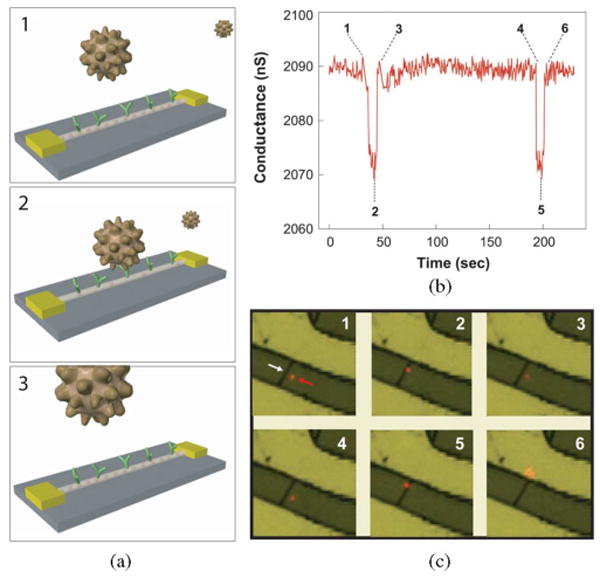
(a) Schematic illustration of a single virus binding and unbinding to the surface of an NWFET modified with antibody receptors. (b) Conductance versus time data recorded from a single device modified with antiinfluenza type A antibody. (c) Optical data recorded simultaneously with conductance data in (b). Combined bright-field and fluorescence images correspond to time points 1–6 indicated in the conductance data; virus appears as a red dot in the images. The white arrow in image 1 highlights the position of the NW, and the red arrow indicates the position of a single virus. Images are 8 × 8 μm. Adapted from [35] (National Academy of Sciences, copyright 2004).
The exquisite sensitivity and selectivity of NWFET detectors was subsequently demonstrated by several groups in the context of protein detection. In 2005 [36], we explored the sensitivity limits of NWFETs functionalized with monoclonal antibodies that were specific to cancer detection markers such as prostate-specific antigen (PSA), as shown schematically in Fig. 3(a). Distinct p- and n-type NW device elements were incorporated in a single chip, and data recorded simultaneously from p-type and n-type devices [see Fig. 3(b)] showed reversible conductance increase and decrease, respectively, during delivery of PSA followed by buffer solution (indicated by the arrows). The data shown represent detection down to 0.9 ng/mL, but detection of PSA is routinely achieved with an SNR>3 for concentrations down to 75 fg/mL, or approximately 2 fM [36]; this represents a sensitivity limit 104–109 times below that afforded by state-of-the-art ion sensitive planar FETs [39]–[41]! It is important to note that these exquisite sensitivities were also verified by a different group in 2007 that used top-down fabricated NWs, demonstrating the broad applicability of nanostructured materials in biological sensing [42].
Fig. 3.
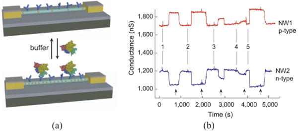
(a) Schematic illustration of an NWFET configured as a protein sensor with antibody receptors (blue). (b) Complementary sensing of PSA using p-type (NW1) and n-type (NW2) devices. Points 1–5 correspond to the addition of PSA solutions of (1, 2) 0.9 ng/mL, (3) 9 pg/mL, (4) 0.9 pg/mL, and (5) 5 ng/mL. Adapted from [36] (Nature Publishing Group, copyright 2005).
B. Advantages of Nanoscale Morphology for Cellular Interfaces
A major advantage of NWFETs relates to the coupling between the NW and cells. The formation of a tight junction between a cell or cellular projections and the semiconductor surface is important in determining sensitivity, i.e., it is important to minimize the junction gap when measuring local field changes given the high ionic strength (ca. 150 mM) of cell culture medium. On a perfectly flat surface, this gap is on the order of tens of nanometers, a result of the finite size of adhesion/transmembrane proteins [18]. NWs, however, are freestanding structures that protrude from the surface of the substrate, and are expected to form naturally tighter junctions with the local cell membrane than is possible with a planar device [see Fig. 4(a)].
Fig. 4.
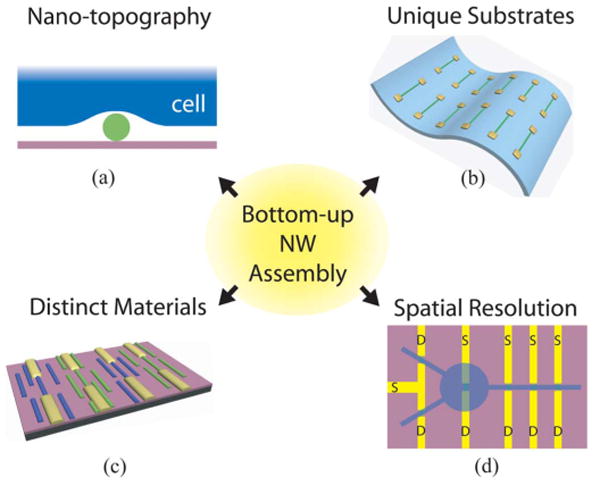
Schematic diagram outlining unique advantages of bottom-up NW assembly, including (a) nanotopographic morphology, (b) ability to assemble devices on flexible, transparent substrates, (c) assembly of distinct NW materials on the same chip, and (d) high spatial resolution of NW devices, where S and D correspond to source and drain electrodes.
Cellular adhesion and guidance may be further enhanced by unique interactions between the nanotopographic surface and cell membrane. For example, intimate contact was recently demonstrated in the case of supported lipid bilayer–carbon nanotube hybrids, where a nanotube was shown to act as a barrier to the diffusion of membrane-bound proteins [43]. In the specific case of cells, it has been demonstrated that nanostructured surfaces formed by carbon nanotube networks or etched silica promote cellular adhesion, spreading, and guidance, even in the absence of conventional adhesion factors such as polylysine [44]–[47]. Dense, freestanding arrays of semiconductor NWs have been shown to be biocompatible substrates that can actually promote filopodia formation and axonal outgrowths [48], [49]. Moreover, sparse NWs arrays were shown to direct axonal growth over large areas and with high spatial resolution; these arrays in fact promoted the formation of focal adhesions, which are critical for tight cell–substrate junctions [50]. Taken together, these findings indicate that NWFETs could serve not only as sensitive electronic devices, but also as nanoscale interfaces that promote unique and favorable substrate–cell interactions.
One final aspect of nanostructured surfaces that warrants emphasis is their effect on ion-channel function. Two separate groups demonstrated that neurons cultured on CNT mats exhibit enhanced spiking activity (versus those cultured on planar control surfaces), and suggest that the conductive, nanostructured surface enhances membrane excitability [51], [52]. Whereas these studies warrant further mechanistic investigations, they provide additional evidence that nanostructured surfaces form unique interactions with the cell membranes that have not been realized in the context of planar electronic devices.
II. Device Fabrication
Our method of bottom-up assembly involves growth of NWs by the well-established nanocluster-catalyzed vapor–liquid–solid technique [22]–[24], assembly of the NWs on a substrate, then interconnection and metallization using lithography [53]. A true advantage of this technique, which outlines a strength of bottom-up assembly in general, is that NWs can be assembled on nearly any type of surface, including those that are typically not compatible with standard CMOS processing, such as flexible plastic substrates [see Fig. 4(b)] [54]–[56]. A second advantage is that sequential patterning and assembly steps enable fabrication of distinct NW devices on a substrate, as indicated by the blue and green NWs in Fig. 4(c). Similar or distinct NWs, such as p- and n-type materials, can thus be readily fabricated into functional device arrays using photo- or electron-beam lithography, followed by metallization and dielectric passivation of the metal regions [53].
A. NWFET Fabrication
Device arrays are fabricated by aligning NWs on the surface of a substrate using either fluid-based or contact printing techniques [54], [57]. Both methods yield highly aligned NWs with pitch that can be rationally varied between tens of microns to as small as tens of nanometers. Interconnects are defined lithographically, then metallized to form Ohmic contacts with the NWs [53]. Using this method, tens or more devices can be obtained on a single chip, enabling many experiments to be attempted in parallel. The device pitch is defined by NW spacing and the design of the lithography pattern; device arrays with pitches from more than 50 μm to 400 nm and below have been designed using this approach [57], [58]. Notably, these high-density arrays enable electronic interfaces to individual subcellular features, such as axons and dendrites; this spatial resolution is difficult to achieve by other conventional means [see Fig. 4(d)].
B. Device Characteristics
Fig. 5 shows conductance versus water-gate measurements [53] for three typical NW devices submerged in electrophysiology medium [56]. The conductance (G) versus water-gate voltage (Vg) data show that the p-type NW devices all turn off (exhibit threshold voltages) close to or positive of Vg = 0. In the on-state, the maximum device sensitivities, dG/dVg, at Vg = −0.2 are 23, 32, and 22 μS/V for the devices represented by the red, green, and blue traces, respectively.
Fig. 5.
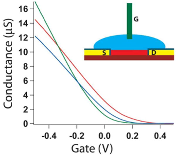
Conductance versus water-gate voltage for three representative NWFET devices. Inset: Scheme representing experimental setup, which includes: (red) NW, (yellow/navy) passivated contact electrodes, (blue) electrolyte solution, and (green) Ag/AgCl reference/gate electrode.
III. NW–Neuron Interfaces
A. Surface Patterning
Efficient design of hybrid nanoscale nanoelectronic/neuron interfaces requires a surface-patterning scheme that incorporates both cellular attachment factors at the devices and cell adhesion sites and inert regions elsewhere on the chip. This method of heterogeneous patterning can be utilized to achieve neuronal adhesion and growth across one or many NW devices, while preventing unwanted adsorption on other regions of the chip. In several recent studies [59]–[61], sparsely plated neurons were cultured on patterned polylysine, with neurite growth guided along micropatterned lines. The neurons were viable for up to 17 days and exhibited healthy electrophysiological properties and synaptic connections. These findings provide strong support that healthy micropatterned neurons also can be incorporated into neuron/NW hybrid devices with high yield.
In the specific case of neuron/NW studies [58], surfaces were patterned after device fabrication using a two-step process. First, the surface was reacted with a fluorinated silane, which is known to form one of the most hydrophobic self-assembled monolayers achievable on a smooth surface [62], and is therefore, effective at preventing cell adhesion. Photolithography followed by poly-d-lysine adsorption and removal of the resist yielded distinct regions of attachment factor. Fig. 6(a) represents a pattern that includes regions for soma adhesion and narrow lines designed to direct neurite growth across single NW devices. Microscopy of a fixed culture [see Fig. 6(b)] reveals that neurite growth is confined to the patterned lines and that a good yield of neurite/NW junctions can be achieved.
Fig. 6.
NW/neuron interfaces. (a) Schematic of interconnected neuron motif and (b) SEM image of fixed neurons exhibiting a neural network where multiple neurites are interfaced with (red arrows) NW devices. Inset: Zoom depicting an axon (denoted by yellow dotted lines) guided between source and drain electrodes across an NWFET (highlighted by blue arrow).
B. Characterization of NW/Neuron Interfaces
We assessed the ability of NWs to record extracellular field changes by fabricating arrays of hybrid devices consisting of distinct soma with axonal growth guided across single NW devices [see Fig. 7(a)] [58]. Fig. 7(b) shows the behavior of one of these devices, which exhibits good temporal correlation between IC potentials and the signal recorded by the interfaced p-type NWFET. The direct correlation between the IC and p-type NW trace indicates that depolarization results in negative charging of the extracellular space around the NW. This is expected in cases where the membrane expresses a relatively high Na+ ion-channel density [33] (known to be the case in mammalian neurons, and axons in particular [63]–[65]) and is consistent with observations from mammalian neurons interfaced with planar FETs [19]. One important point to note is that the typical active junction area for NW/axon interfaces is 0.01–0.02 μm2, at least two orders of magnitude smaller than microfabricated electrodes and planar FETs [19]. The high spatial resolution enabled by NWFET interfaces opens up new avenues for multiplexed recordings from single neurons.
Fig. 7.
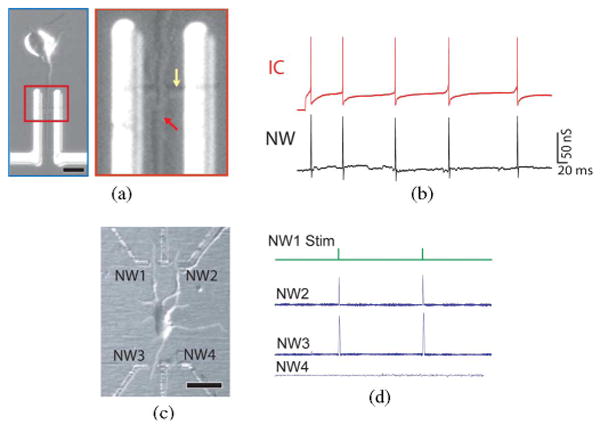
(a) Optical image of a cortical neuron aligned across an NWFET; scale bar is 10 μm. Inset: High-resolution image of region where (red arrow) axon crosses (yellow arrow) an NW. (b, red trace) IC potential of an aligned cortex neuron (after 6 days in culture) during stimulation with a 500-ms-long current injection step of 0.1 nA; (b, black trace) time-correlated signal from axon measured using a p-type NWFET. (c) Optical image of a cortical neuron interfaced to three of the four functional NWFETs in an array; scale bar is 20 μm. (d) Trace of pulses applied to NW1 for antidromic stimulation of the neuron. The response was measured by the NW–dendrite junctions at NW2 and NW3. Adapted from [58] (American Association for the Advancement of Science, copyright 2006).
C. Multiplexed NW/Neuron Interfaces
One example of multiplexed hybrid structures consists of a central cell body and four peripheral SiNWs arranged at the corners of a rectangle; polylysine patterning promotes neurite growth across these elements. A representative optical image [see Fig. 7(c)] shows one NW–axon and two NW–dendrite elements at positions 1, 2, and 3, respectively. This multi-NW–neurite array was used to study spike propagation in the absence of an IC microelectrode with NW1 as a local input to elicit action potential spikes. After stimulation with a biphasic pulse sequence [see Fig. 7(d)], backpropagation of the elicited action potential was detected in the two dendrites crossing elements NW2 and NW3. The lack of observed signal from NW4 demonstrates the absence of crosstalk in the hybrid device array.
IV. NW–Heart Interfaces
Whole tissue, for example, the heart, represents another system where NW devices could be used to collect electrophysiological information. Activation sequences across the surface of the heart have been measured using macroscale metallic electrodes [66], optical microscopy of dyed tissue [6], and MEAs [16], [17], but none of these techniques has been miniaturized to achieve single-cell resolution. However, given the complexities of activation sequences, cellular or subcellular-level interfaces with cardiac tissue could be crucial for better understanding cardiac dysfunction, such as, for example, arrhythmia [3], [67], [68].
A. Characterization of Heart/NW Interface
We used live hearts from embryonic chickens (E10-E15 stage) as a model system for studying tissue/NW interfaces. In a typical experiment with a planar NWFET chip configuration [see Fig. 8(a) and (b)], a freshly isolated heart was placed on top of the active device region of a heated sample chamber [56]. After a brief period of equilibration with electrophysiology medium, hearts beat spontaneously at a typical frequency of 1–3 Hz. Initially, the NWFET response to beating hearts was carried out by simultaneously recording signals from an NWFET and from a conventional glass pipette electrode inserted into the heart. Representative data [see Fig. 8(c)] show close temporal correlation between initial sharp peaks recorded by the two distinct measurements, although the pipette peak occurs ca. 100 ms before the NWFET peak in each beat. The consistent time difference is expected since the pipette was inserted into a spatially remote region with respect to the NWFET devices. Examination of individual NW signals reveals an initial fast phase (full-width at half maximum, FWHM = 6.8 ± 0.7 ms) followed by a slower phase (FWHM = 31 ± 9 ms), where these two phases can be attributed to transient ion-channel current and mechanical motion, respectively. NWFET signals exhibiting the fast followed by slow phases were recorded in 85% of our >75 independent experiments, and thus, demonstrate the reproducibility of our NW-based recording approach for tissue measurements [56].
Fig. 8.
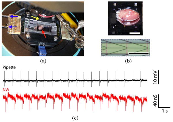
NW/heart interfaces. (a) Experimental setup showing heart on NWFET chip in temperature regulated cell. Arrows show (red) position of heart, (yellow) Ag/AgCl reference electrode, and (blue) source/drain interconnect wires. (b, top) Magnified image of heart on surface of planar chip; scale bar is 4 mm. (Bottom) Zoom of dotted region in upper image showing three pairs of NWFETs; scale bar is 150 μm. (c) Simultaneous recordings from (black trace) a glass pipette and (red trace) an NW device. Adapted from [56] (American Chemical Society, copyright 2009).
The peaks recorded with our NWFETs [see Fig. 8(c)] exhibit excellent S/N. The observed conductance changes associated with these peaks do, however, depend on the device sensitivity. To illustrate this point and provide voltage calibration for the peaks, data were recorded at a variety of applied watergate potentials. NWFET results from a beating heart with the water-gate varied from −0.4 to 0.4 V [see Fig. 9(a) and (b)] show a decrease in the magnitude of the fast transient conductance change from ca. 55 to 11 nS, which is correlated with the decrease in device transconductance over this same range of water-gate potentials. Notably, the voltage-calibrated signal determined using the device transconductance [see Fig. 9(b)] was essentially constant at 5.1 ± 0.4 mV for this same variation of water gate voltage. These results confirm the stability of the interface between the NWFETs and beating heart, and highlight the necessity of recording explicit device sensitivity to interpret corresponding voltages [56].
Fig. 9.
(a) Expansion of single fast transients recorded from a heart for (red) Vg = −0.4 V, (green) 0 V, and (blue) 0.4 V. (b) Plots of (red) peak conductance amplitude and (blue) calibrated peak voltage amplitude versus Vg for same experiment shown in a. Adapted from [56] (American Chemical Society, copyright 2009).
B. Transparent and Flexible Substrates
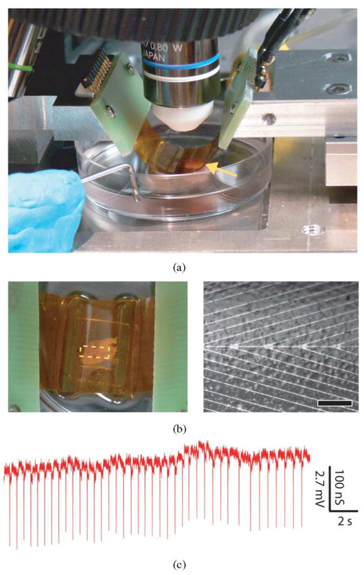
NWs and carbon nanotube FETs can be fabricated on flexible plastic substrates [54], [55], [69], and thus, open up the possibility of making chips that can be readily deformed to tissue and organs or used for in vivo studies, as demonstrated in the case of polymer-based passive MEAs [70], [71]. We have explored this concept by assembling active NWFETs on 50-μm-thick flexible and transparent Kapton substrates. These flexible and transparent NWFET chips enable simultaneous optical imaging and electronic recording in configurations that are not readily accessible with traditional planar device chips, yet advantageous for producing diverse, functional tissue–device interfaces. A bent device chip with concave surface facing a beating heart immersed in medium [see Fig. 10(a)] illustrates this capability. We note that the chip is readily integrated into an upright microscope and allows for both visual inspection, which enables rough orientation of the device array to the heart, and higher resolution imaging through the transparent substrate while recording from NWFET devices [see Fig. 10(b)]. Our capacity for simultaneous imaging of tissue and devices enables their registration at the level of the entire organ down to that of individual cells. Notably, recording from a representative NWFET device in this inverted configuration [see Fig. 10(c)] demonstrated excellent S/N peaks correlated with the spontaneously beating heart. The average magnitude of the conductance peaks, 164 ± 7 nS, and calibrated voltage, 4.5 ± 0.2 mV, are similar to that recorded in more traditional “planar” configuration. In addition, similar recording was achieved on beating hearts in which bent chips were oriented with convex NWFET surface wrapped partially around the heart. Taken together, these results demonstrate that our flexible and transparent NW chips can be used to record electronic signals from organs in configurations not achievable by conventional electronics [56].
Fig. 10.
(a) (Yellow arrow) Heart located underneath bent substrate with NWFETs on the lower concave face of the substrate. (b, left) Top-down photograph of same system, which enables overall registration between heart and lithographically defined markers on the substrate. (Right) Optical image taken with same system showing features on the heart surface versus position of individual NW devices, which are located along the central horizontal axis. Scale bar is 150 μm. (c) Recorded conductance data from an NWFET in the configuration shown in (a). Adapted from [56] (American Chemical Society, copyright 2009).
V. NW–Cardiomyocyte Interfaces
Our studies of neurons [58] and heart tissue [56] demonstrate that NW devices can be used as a general platform to investigate electrogenic biological systems. A separate group also demonstrated that lithographically patterned top-down NWFETs can be used to record signals from rat cardiomyocytes and monolayers of rat aortic smooth muscle cells with high S/N and millivolts amplitudes [72]. In our own laboratory, we investigated cultured cardiomyocyte monolayers in a new manner and probed the relationship between interfaces and signal magnitude [73]. This relationship, though never studied in the context of NW devices, is critical to understand given the unique interactions that exist between cells and nanoscale structures [45]–[52].
A. Characterization of NW/Cardiomyocyte Interfaces
We developed a flexible scheme for interfacing cardiomyocytes and cells in general with NWFETs. Chips were fabricated using the same process used for neuron and heart studies [56], [58] [see Fig. 11(a)]. Separately, embryonic chicken cardiomyocytes were cultured on 100–500-μm-thick, optically transparent and flexible pieces of polydimethylsiloxane (PDMS) [see Fig. 11(b)] to form cell monolayers, and then a PDMS/cardiomyocyte substrate was transferred into a well, which contained extracellular medium, over the NWFET chip [see Fig. 11(c)]. PDMS/cardiomyocyte cell substrates were positioned using an x–y–z manipulator under an optical microscope to bring spontaneously beating cells into direct contact with the NWFETs [see Fig. 11(d)]. This approach enabled us to contact specific monolayer regions with specific devices, and subsequently change the region that was being monitored with the NWFETs.
Fig. 11.
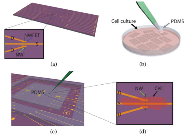
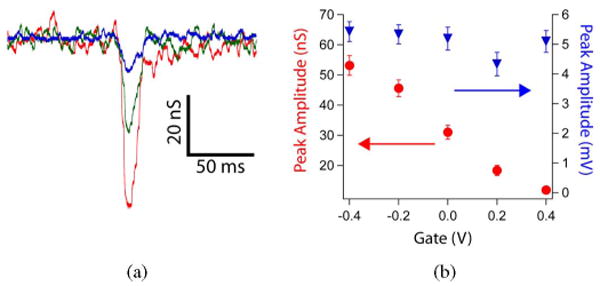
(A) NWFET chip, where NW devices are located at the central region of chip. The visible linear features (gold) correspond to NW contacts and interconnect metal. Zoom-in showing a source (S) and two drain (D) electrodes connected to a vertically oriented NW (blue arrow) define two NWFETs. (b) Cardiomyocytes cultured on thin flexible pieces of PDMS, where (green) one piece is being removed with tweezers. (c) PDMS substrate with cultured cells oriented over the device region of the NWFET chip. The green needle-like structure indicates the probe used to both manipulate the PDMS/cell substrate to specific NW device locations. (d) Schematic of (black arrow) a cardiomyocyte oriented over (green arrow) an NW device. Adapted from [73] (National Academy of Sciences, copyright 2009).
The ability to manipulate the PDMS/cell substrate independent of the NWFET chip also enables us to identify specific cardiomyocyte regions using an optical microscope, place the desired cell or cell network over NWFET devices, and then record from the desired region. Two examples are shown in Fig. 12. In the first case, a patch of spontaneously beating cells was located [red dashed line, see Fig. 12(a)] and placed over a specific device [yellow arrow, see Fig. 12(a)]. Conductance versus time data recorded was then recorded [see Fig. 12(b)], and yielded an average signal amplitude of 53.2 ± 4.0 nS and relatively large calibrated voltage of 4.2 ± 0.3 mV. In a second example, a comparatively distinct cell in a cardiomyocyte monolayer was located [red dashed line, see Fig. 12(c)] and placed over a different device [yellow arrow, see Fig. 12(c)]. The recorded conductance versus time data from the spontaneously beating cell yielded an average amplitude of 19.1 ± 3.1 nS and 2.1 ± 0.3 mV [see Fig. 12(d)]. Importantly, our ability to identify and register specific cellular regions over NWFET elements has not been demonstrated previously for either planar or nanoscale FET where cells have been cultured directly over device chips. This capability opens up the possibility of a number of interesting studies in the future, including multiplexed recording from well-defined multicellular configurations as well as multiplexed measurements at the single cell level for subcellular resolution investigations.
Fig. 12.
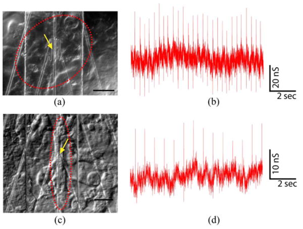
(a) Patch of (red dashed oval) beating cells over (yellow arrow) an NWFET; scale bar is 40 μm. (b) Conductance versus time signals recorded from this cell patch. (c) Distinct patch of (red dashed oval) beating cells over (yellow arrow) an NW device; scale bar is 20 μm. (d) Conductance versus time signals recorded from the cells. Adapted from [73] (National Academy of Sciences, copyright 2009).
These basic results for NWFET recording from PDMS/cardiomyocyte samples can be compared to previous studies of cardiomyocytes. For example, studies of cardiomyocyte monolayers cultured on conventional planar FET devices have yielded peaks with S/N of 2–6 and amplitudes from 0.2 to 2.5 mV [12], [13]. In general, our NWFETs yield better S/N with values >4 and a maximum of 25 observed (see Section B). In addition, the typical calibrated voltages recorded in our measurements are similar to or greater than the largest values reported previously. The improvement in peak amplitude is consistent with the fact that the nanodevices protrude from the plane of substrate, and hence, can increase NW/cell interfacial coupling [43]–[52], an observation that is consistent with previous reports by us and others on cultured neurons [58], embryonic hearts [56], and muscle cells [72].
B. Cell Substrate Displacement Experiments
The ability to manipulate the PDMS/cell substrate independent of the NWFET chip also opens up new opportunities compared with cells cultured directly on device arrays. For example, we have carried out experiments to investigate the relationship between recorded signal magnitude and NWFET-PDMS/cell by using a micropipette to displace the PDMS a fixed distance as represented schematically in Fig. 13(a). Representative conductance versus time data recorded from a spontaneously beating cardiomyocyte monolayer using the same NWFET device exhibited an increase in peak amplitude from 44 ± 3 to 72 ± 4 nS as the PDMS was displaced 9.8 μm toward the device. We note in both positions shown that the changes in NWFET/cell interface are stable. A direct comparison of single peaks recorded for ΔZ values of 0, 8.2, 13.1, and 18.0 μm shows a consistent monotonic increase in peak amplitudes from 31 to 72 nS. In addition, this high-resolution peak comparison demonstrates that there is no observable change in peak shape or peak width over this >2x change in amplitude, and that the peak width is consistent with time scales for ion fluxes associated with ion-channels opening/closing [12].
Fig. 13.
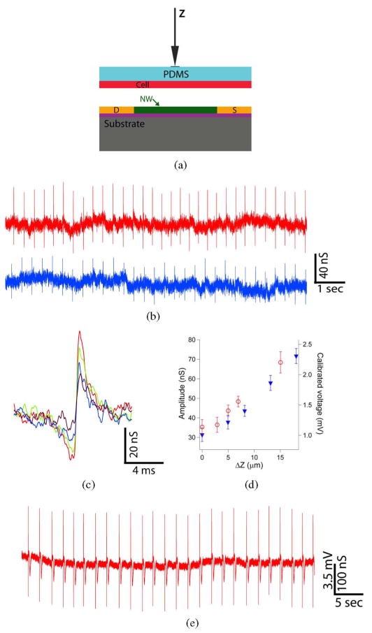
(a) Schematic illustrating displacement (Z) of the PDMS/cell substrate with respect to an NWFET device. (b) Two representative traces recorded with same device for ΔZ values of (blue) 8.2 μm and (red) 18.0 μm. (c) High-resolution comparison of single peaks recorded with ΔZ values of (purple) 0, (blue) 8.2 (blue), (green) 13.1, and (red) 18.0. (d) Summary of the recorded conductance signals and calibrated voltages versus ΔZ, where the open red circles (filled blue triangles) were recorded for increasing (decreasing) ΔZ. (e) Data recorded in distinct experiment at ΔZ close to cell failure. Adapted from [73] (National Academy of Sciences, copyright 2009).
A plot of our experimental results [see Fig. 13(d)] summarizes clearly the systematic 2.3-fold increase in conductance and calibrated voltage peak amplitude, and moreover, demonstrates these amplitude changes are reversible for experimental data recording on increasing and decreasing PDMS displacement. Last, separate experiments designed to push the limits of PDMS/cell displacement [see Fig. 13(e)] showed very large conductance versus time peaks with average conductance amplitude of 299 ± 7 nS and calibrated voltage of 10.5 ± 0.2 mV. These results were very stable suggesting no adverse affect on the cardiomyocytes, although even larger displacements could ultimately lead to irreversible changes and cessation of spontaneous beating. Recent studies of Aplysia neurons cultured on planar FET devices have also reported an increase in peak amplitude when the cell body was displaced [15]. In both cases, the enhanced signal amplitudes can be attributed to a decrease in gap between the cell membrane and devices, although future studies will be needed to quantify such junction changes.
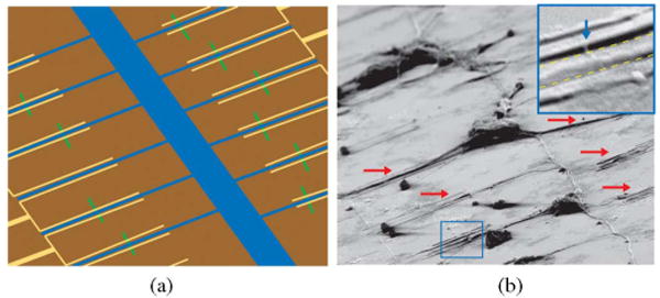
C. Multiplexed Recording With NWFETs
Multiplexed measurements from NWFET arrays have been reported previously in the context of other biological systems [35], [36], [42], [56], [58]. To this end, we carried out multiplexed measurements using the NWFET arrays interfaced with cardiomyocytes. The devices used in these studies were configured in a linear array [see Fig. 14(a)] with an average spacing of 300 μm so that signal propagation within cardiomyocyte monolayers could be characterized. Simultaneous recording from NW1, NW2, and NW3 devices in contact with spontaneously beating monolayer [see Fig. 14(b)] yield very stable and high S/N (∼10) peaks with amplitudes of 50 ± 5, 43 ± 3, and 102 ± 15 nS, respectively. Using the individually characterized sensitivities for NW1, NW2, and NW3 further give calibrated voltages of 4.6 ± 0.4, 4.0 ± 0.3, and 5.9 ± 0.9 mV, respectively, where the relative large magnitude indicates a good junction is formed between each of the NWFETs and PDMS/cell substrate in the experiment. To determine robustly the time differences between the signals recorded by the three devices we used a cross-correlation methodology [74], [75], although the time difference can also be roughly estimated from comparison single peaks from the three devices, as shown in Fig. 14(b). The time shifts between devices derived from the cross-correlation analysis of the full data traces show that the average time delay between NW1 and NW2, NW1 and NW3, and NW2 and NW3 is 1.4 ± 0.3, 5.6 ± 0.2, and 4.3 ± 0.3 ms, respectively. These results and device separations yield propagation speeds of 0.07–0.21 m/s that are consistent with other measurement on monolayers of neonatal rat cardiomyocytes [76]. The variation in propagation speeds is not surprising given the monolayer inhomogeneity and suggests an important future direction. Specifically, high-resolution multiplexed NWFET recording combined with optical imaging will enable details of both intra- and intercellular propagation to be characterized for well-defined cellular structures.
Fig. 14.
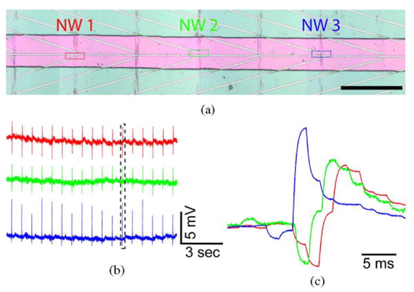
(a) Optical micrograph showing three NWFET devices (NW1, NW2, and NW3) in a linear array, where pink indicates the area with exposed NW devices; scale bar is 150 μm. (b) Representative conductance versus time signals recorded simultaneously from NW1, NW2, and NW3. (c) High-resolution comparison of the temporally correlated peaks highlighted by the black dashed box in (b). Adapted from [73] (National Academy of Sciences, copyright 2009).
VI. Conclusion and Prospects
In recent years, NW devices have been implemented as a broad platform to electronically interface with cells and tissue, demonstrating several key points. First, NWFETs were used to measure signals from individual cells and tissue. Calibrated signals measured by two different groups were consistently in millivolts range [56], [58], [72], [73]. These signals are considerably larger than those measured using planar, lithographically patterned FETs or MEAs [8]–[21], possibly because of enhanced coupling between the nanoscale device and cell membrane. This important issue of signal magnitude was subsequently investigated by confirming a direct correlation between signal magnitude and (a) device sensitivity (transconductance) [56], [73] and (b) interface quality between cells and substrate [73]. A second distinct point relates to spatial resolution. NW devices were used to connect with individual neurons at the level of individual axons or dendrites [58], and with heart tissue [56] or cardiomyocytes at the subcellular level. The ultimate device pitch, which has been demonstrated at the submicron level [58] and could be reduced to as small as tens of nanometers, is much better than has been demonstrated with lithographically defined devices [8]–[20] or with optical techniques [3]. Multiplexed recording from these devices has subsequently enabled signal mapping in the context of neurons, heart tissue, and cardiomyocytes [56], [58], [73].
The methods presented in this study represent a general and flexible approach for creating hybrid nanoelectronic–biological devices that could serve as the foundation for new, fundamental studies and novel directions in biomedical research and applications, as summarized in Fig. 15. A remarkable property of NWs, at the most fundamental level, is that their material composition and corresponding properties can be tuned at the time of synthesis. This opens up future opportunities in the design of ultrahigh sensitivity transistors through band structure engineering [23], [28], incorporation of photonic materials for light-addressable interfaces with photoactive cells [77], or use of novel geometries (e.g. branched NWs [78], [79]) to further improve device-membrane coupling.
Fig. 15.
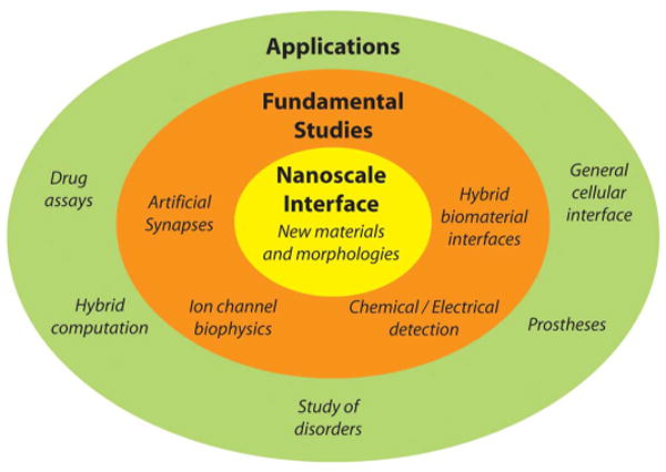
Overview of a bottom-up paradigm for NW nanobioelectronic interfaces.
Although the nanostructures reviewed in this article have been used as extracellular interfaces, NWs are also particularly well suited for IC measurements because of their 1D morphology. In recent studies, mammalian cells were cultured on vertical, freestanding arrays of Si or GaP NWs; many of the NWs penetrated the cell membrane, accessing the IC region. Cells cultured in this fashion remained viable for at least several days [48], [49]. Arrays of suspended or vertical, freestanding NW transistors [80]–[82] could be used to obtain multiplexed IC data, a feat that cannot be easily accomplished using conventional patch clamp electrophysiology [1]–[4], or might be used for IC stimulation.
Elaboration on the modes of NW detection represents another direction of basic research. For example, nanoscale sensors have already been used to detect the release of chromogranin A from the presynaptic terminal of neurons [83], secretion of the enzyme metalloprotease 9 from human macrophages, [84], and acidification near T-cells after an immune response [85]. In the future NW device arrays might be used to correlate electronic signaling with chemical release or could be used to simultaneously detect a matrix of biologically relevant species. These techniques, which would push the boundaries of present technologies, could lead to new drug assays or breakthroughs in fundamental bioscience.
Finally, NWs could serve as a foundation for new and powerful prosthetic devices. Significantly, NW devices could be assembled on biocompatible substrates for long-term implants that might avoid issues that exist with conventional devices, such as delamination of the metallic electrode surface and inflammation and astrocyte accumulation at the site of the surrounding tissue [86]–[89]. NW devices that form intimate extracellular or IC connections with excitable cells and tissue might furthermore be used for functional prosthetics, which could complement current technology used to address problems such as spinal cord injuries [90] and blindness [91], [92].
Biographies

Brian P. Timko received the B.S. degree in chemistry and chemical engineering from Lehigh University, Bethlehem, PA, in 2002, and the Ph.D. degree in chemistry from Harvard University, Cambridge, MA, in 2009.
He is currently a Postdoctoral Fellow at Massachusetts Institute of Technology, Cambridge. His current research interests include nanowire synthesis along with structural and electrical characterization, design of electrical interfaces between nanowires and cells and tissue, and the use of nanotechnology, in general, to solve biological problems.
Dr. Timko received the Gold Award from the Materials Research Society in 2008, was a finalist in the National Collegiate Inventors Competition in 2007, and received the William H. Peterson Award from the American Chemical Society in 2006. He was a National Science Foundation Graduate Research Fellow.
Tzahi Cohen-Karni received both the B.Sc. degree in materials engineering and the B.A. degree in chemistry from the Technion Israel Institute of Technology, Haifa, Israel, in 2004, and the M.Sc. degree in chemistry from Weizmann Institute of Science, Rehovot, Israel, in 2006. He is currently working toward the Ph.D. degree at the School of Engineering and Applied Sciences, Harvard University, Cambridge, MA.
His current research interests include the unique interfaces between biology and nanotechnology, namely interfacing tissue and cells with nanostructures and monitoring their electrical properties.
Mr. Cohen-Karni received the Feinberg Award of excellence from Weizmann Institute of Science in 2006.

Quan Qing received the B.S. and Ph.D. degrees in chemistry from Peking University, Beijing, China.
He is currently a Postdoctoral Fellow in the Department of Chemistry and Chemical Biology, Harvard University, Cambridge, MA. His research interests include novel biochemical sensors based on nanowires, which could be interfaced with live cells and tissues to study biological signals in functional networks.

Bozhi Tian received the B.S. degree in chemistry and the M.S. degree in inorganic chemistry from Fudan University, Shanghai, China, and the M.S. degree in physical chemistry from Harvard University, Cambridge, MA, where he is currently working toward the Ph.D. degree.
His current research interests include the fundamental study of high performance nanowire photovoltaics and the application of novel nanowire devices in cells and tissue.
Mr. Tian received the American Chemical Society Division of Inorganic Chemistry's Young Investigator Award and the Chinese Government Award for Outstanding Students Studying Abroad in 2009, and received Silver Award from the Materials Research Society in 2008.
Charles M. Lieber (M'09) received the Ph.D. degree in chemistry from Stanford University, Stanford, CA, in 1985.
He is currently the Mark Hyman Professor in the Department of Chemistry and Chemical Biology and holds a joint appointment in the Division of Engineering and Applied Sciences. His current research interests include the chemistry and physics nanoscale materials, rational synthesis of new nanoscale materials, development of methodologies for hierarchical assembly of functional nanosystems, fundamental electronic, optical, and optoelectronic properties of nanoscale materials, design and development of nanoelectronics and nanophotonic systems with emphasis on digital computing and nanoenabled photovoltaics, nanoelectronic–biology interfaces with emphasis on real-time, ultrasensitive biodetectors, new tools for neuroscience and cell biology, and novel nanoelectronic interfaces to tissue and organs.
Dr. Lieber received the Pioneer Award from the National Institutes of Health in 2008, is an elected Fellow of the American Chemical Society, the American Physical Society and Materials Research Society, and is a member of the National Academy of Sciences.
Contributor Information
Brian P. Timko, Email: brian@cml.harvard.edu, Department of Chemistry and Chemical Biology, Harvard University, Cambridge, MA 02138 USA. He is now with Massachusetts Institute of Technology, Cambridge, MA 02139 USA.
Tzahi Cohen-Karni, Email: tzahi@cml.harvard.edu, School of Engineering and Applied Sciences, Harvard University, Cambridge, MA 02138 USA.
Quan Qing, Email: quanqing@cml.harvard.edu, Department of Chemistry and Chemical Biology, Harvard University, Cambridge, MA 02138 USA.
Bozhi Tian, Email: tianbz@cml.harvard.edu, Department of Chemistry and Chemical Biology, Harvard University, Cambridge, MA 02138 USA.
Charles M. Lieber, Email: cml@cml.harvard.edu, Department of Chemistry and Chemical Biology and School of Engineering and Applied Sciences, Harvard University, Cambridge, MA 02138 USA.
References
- 1.Hille B. Ion Channels of Excitable Membranes. Sunderland, MA: Sinauer; 2001. [Google Scholar]
- 2.Zipes DP, Jalife J. Cardiac Electrophysiology: From Cell to Bedside. Philadelphia, PA: Saunders; 2004. pp. 169–253. [Google Scholar]
- 3.Dhein S, Mohr FW, Delmar M. Practical Methods in Cardiovascular Research. Berlin, Germany: Springer-Verlag; 2005. pp. 215–453. [Google Scholar]
- 4.Davie JT, Kole MHP, Letzkus JJ, Rancz EA, Spruston N, Stuart GJ, Häusser M. Dendritic patch-clamp recording. Nat Protocols. 2006;1(3):1235–1247. doi: 10.1038/nprot.2006.164. [DOI] [PMC free article] [PubMed] [Google Scholar]
- 5.Zochowski M, Wachowiak M, Falk CX, Cohen LB, Lam YW, Antic S, Zecevic D. Concepts in imaging and microscopy - Imaging membrane potential with voltage-sensitive dyes. Biol Bull. 2000;198(1):1–12. doi: 10.2307/1542798. [DOI] [PubMed] [Google Scholar]
- 6.Efimov IR, Nikolski VP, Salama G. Optical imaging of the heart. Circ Res. 2004;95(1):21–33. doi: 10.1161/01.RES.0000130529.18016.35. [DOI] [PubMed] [Google Scholar]
- 7.Kléber AG, Rudy Y. Basic mechanisms of cardiac impulse propagation and associated arrhythmias. Physiol Rev. 2003;84(2):431–488. doi: 10.1152/physrev.00025.2003. [DOI] [PubMed] [Google Scholar]
- 8.Halbach MD, Egert U, Hescheler J, Banach K. Estimation of action potential changes from field potential recordings in multicellular mouse cardiac myocyte cultures. Cell Physiol Biochem. 2003;13(5):271–284. doi: 10.1159/000074542. [DOI] [PubMed] [Google Scholar]
- 9.Meyer T, Boven KH, Gunther E, Fejtl M. Micro-electrode arrays in cardiac safety pharmacology: A novel tool to study QT interval prolongation. Drug Safety. 2004;27(11):763–772. doi: 10.2165/00002018-200427110-00002. [DOI] [PubMed] [Google Scholar]
- 10.Erickson J, Tooker A, Tai YC, Pine J. Caged neuron MEA: A system for long-term investigation of cultured neural network connectivity. J Neurosci Method. 2008;175(1):1–16. doi: 10.1016/j.jneumeth.2008.07.023. [DOI] [PMC free article] [PubMed] [Google Scholar]
- 11.Law JKY, Yeung CK, Hofman B, Ingebrandt S, Rudd JA, Offenhäusser A, Chan M. The use of microelectrode array (MEA) to study the protective effects of potassium channel openers on metabolically compromised HL-1 cardiomyocytes. Physiol Meas. 2009;30(2):155–167. doi: 10.1088/0967-3334/30/2/004. [DOI] [PubMed] [Google Scholar]
- 12.Ingebrandt S, Yeung CK, Krause M, Offenhausser A. Cardiomyocyte–hybrids for sensor application. Biosens Bioelectron. 2001;16(7–8):565–570. doi: 10.1016/s0956-5663(01)00170-1. [DOI] [PubMed] [Google Scholar]
- 13.Yeung CK, Ingebrandt S, Krause M, Offenhausser A, Knoll W. Validation of the use of field effect transistors for extracellular signal recording in pharmacological bioassays. J Pharmacol Toxicol Methods. 2001;45(3):207–214. doi: 10.1016/s1056-8719(01)00150-2. [DOI] [PubMed] [Google Scholar]
- 14.Cohen A, Shappir J, Yitzchiak S, Spira ME. Experimental and theoretical analysis of neuron-transistor hybrid electrical coupling: The relationships between the electro-anatomy of cultured Aplysia neurons and the recorded field potentials. Biosens Bioelectron. 2006;22(6):656–663. doi: 10.1016/j.bios.2006.02.005. [DOI] [PubMed] [Google Scholar]
- 15.Cohen A, Shappir J, Yitzchaik S, Spira ME. Reversible transition of extracellular field potential recordings of action potentials generated by neurons grown on transistors. Biosens Bioelectron. 2008;23(6):811–819. doi: 10.1016/j.bios.2007.08.027. [DOI] [PubMed] [Google Scholar]
- 16.Lu ZL, Pereveraev A, Liu HL, Weiergräber M, Henry M, Krieger A, Smyth N, Hescheler J, Schneider T. Arrhythmia in isolated prenatal hearts after ablation of the Cav2.3 (α1E) subunit of voltage-gated Ca2+ channels. Cell Physiol Biochem. 2004;14(1/2):11–22. doi: 10.1159/000076922. [DOI] [PubMed] [Google Scholar]
- 17.Reppel M, Pillekamp F, Lu ZJ, Halbach M, Brockmeier K, Fleischmann BK, Hescheler J. Microelectrode arrays: A new tool to measure embryonic heart activity. J Electrocardiol. 2004;37:104–109. doi: 10.1016/j.jelectrocard.2004.08.033. [DOI] [PubMed] [Google Scholar]
- 18.Fromherz P. Electrical interfacing of nerve cells and semiconductor chips. ChemPhysChem. 2002;2(3):276–284. doi: 10.1002/1439-7641(20020315)3:3<276::AID-CPHC276>3.0.CO;2-A. [DOI] [PubMed] [Google Scholar]
- 19.Voelker M, Fromherz P. Signal transmission from individual mammalian nerve cell to field-effect transistor. Small. 2005;1(2):206–210. doi: 10.1002/smll.200400077. [DOI] [PubMed] [Google Scholar]
- 20.Prohaska OJ, Olcaytug F, Pfundner P, Dragaun H. Thin-film multiple electrode probes: possibilities and limitations. IEEE Trans Biomed Eng. 1986 Feb;BME-33(2):223–229. doi: 10.1109/TBME.1986.325894. [DOI] [PubMed] [Google Scholar]
- 21.Banks DJ, Balachandran W, Richards PR, Ewins D. Instrumentation to evaluate neural signal recording properties of micromachines microelectrodes inserted in invertebrate nerve. Physiol Meas. 2002;23(2):437–448. doi: 10.1088/0967-3334/23/2/317. [DOI] [PubMed] [Google Scholar]
- 22.Hu JT, Odom TW, Lieber CM. Chemistry and physics in one dimension: Synthesis and properties of nanowires and nanotubes. Acc Chem Res. 1999;32(5):435–445. [Google Scholar]
- 23.Lu W, Lieber CM. Semiconductor nanowires. J Phys D: Appl Phys. 2006;39(21):R387–R406. [Google Scholar]
- 24.Agarwal R, Lieber CM. Semiconductor nanowires: optics and optoelectronics. Appl Phys A. 2006;85(3):209–215. [Google Scholar]
- 25.Yang P. The chemistry and physics of semiconductor nanowires. MRS Bull. 2005;30(2):85–91. [Google Scholar]
- 26.Lieber CM, Wang ZL. Functional nanowires. MRS Bull. 2007;32(2):99–104. [Google Scholar]
- 27.Thelander C, Agarwal P, Brogersma S, Eymery J, Feiner LF, Forchel A, Scheffler M, Riess W, Ohlsson BJ, Gosele U, Samuelson L. Nanowire-based one-dimensional electronics. Mater Today. 2006;9(10):28–35. [Google Scholar]
- 28.Lu W, Lieber CM. Nanoelectronics from the bottom up. Nat Mater. 2007;6(11):841–850. doi: 10.1038/nmat2028. [DOI] [PubMed] [Google Scholar]
- 29.Wang ZL. Novel nanostructures of ZnO for nanoscale photonics, optoelectronics, piezoelectricity, and sensing. Appl Phys A. 2007;88(1):7–15. [Google Scholar]
- 30.Dong Y, Tian B, Kempa TJ, Lieber CM. Coaxial group III-nitride nanowire photovoltaics. Nano Lett. 2009;9(5):2183–2187. doi: 10.1021/nl900858v. [DOI] [PubMed] [Google Scholar]
- 31.Cui Y, Lieber CM. Functional nanoscale electronic devices assembled using silicon nanowire building blocks. Science. 2001;291(5505):851–853. doi: 10.1126/science.291.5505.851. [DOI] [PubMed] [Google Scholar]
- 32.Friedman RS, McAlpine MC, Ricketts DS, Ham D, Lieber CM. High-speed integrated nanowire circuits. Nature. 2005;434(7037):1085. doi: 10.1038/4341085a. [DOI] [PubMed] [Google Scholar]
- 33.Tian B, Kempa TJ, Lieber CM. Single nanowire photovoltaics. Chem Soc Rev. 2009;38(1):16–24. doi: 10.1039/b718703n. [DOI] [PubMed] [Google Scholar]
- 34.Cui Y, Wei Q, Park H, Lieber CM. Nanowire nanosensors for highly selective detection of biological and chemical species. Science. 2001;293(5533):1289–1292. doi: 10.1126/science.1062711. [DOI] [PubMed] [Google Scholar]
- 35.Patolsky F, Zheng G, Hayden O, Lakadamyali M, Zhuang X, Lieber CM. Electrical detection of single viruses. Proc Nat Acad Sci USA. 2004;101(39):14017–14022. doi: 10.1073/pnas.0406159101. [DOI] [PMC free article] [PubMed] [Google Scholar]
- 36.Zheng G, Patolsky F, Cui Y, Wang WU, Lieber CM. Multiplexed electrical detection of cancer markers with nanowire sensor arrays. Nat Biotechnol. 2005;23(10):1294–1301. doi: 10.1038/nbt1138. [DOI] [PubMed] [Google Scholar]
- 37.Sze SM, Ng KK. Physics of Semiconductor Devices. Hoboken, NJ: Wiley; 2007. pp. 293–373. [Google Scholar]
- 38.Movileanu L, Howorka S, Braha O, Bayley H. Detecting protein analytes that modulate transmembrane movement of a polymer chain within a single protein pore. Nat Biotechnol. 2000;18(10):1091–1095. doi: 10.1038/80295. [DOI] [PubMed] [Google Scholar]
- 39.Schöning MJ, Poghossian A. Recent advances in biologically sensitive field-effect transistors (BioFETs) Analyst. 2002;127(9):1137–1151. doi: 10.1039/b204444g. [DOI] [PubMed] [Google Scholar]
- 40.Soldatkin AP, Montoriol J, Sant W, Martelet C, Jaffrezic-Renault N. A novel urea sensitive biosensor with extended dynamic range based on recombinant urease and ISFETs. Biosens Bioelectron. 2003;19(2):131–135. doi: 10.1016/s0956-5663(03)00175-1. [DOI] [PubMed] [Google Scholar]
- 41.Sant W, Pourciel-Gouzy ML, Launay J, Conto TD, Colin R, Martinez A, Temple-Boyer P. Development of a creatinine-sensitive sensor for medical analysis. Sens Actuators B Chem. 2004;103(1/2):260–264. [Google Scholar]
- 42.Stern E, Klemic JF, Routenberg DA, Wyrembak PN, Turner-Evans DB, Hamilton AD, LaVan DA, Fahmy TM, Reed MA. Label-free immunodetection with CMOS-compatible semiconducting nanowires. Nature. 2007;445(7127):519–522. doi: 10.1038/nature05498. [DOI] [PubMed] [Google Scholar]
- 43.Zhou X, Moran-Mirabal JM, Craighead HG, McEuen PL. Supported lipid bilayer/carbon nanotube hybrids. Nat Nanotechnol. 2007;2(3):185–190. doi: 10.1038/nnano.2007.34. [DOI] [PubMed] [Google Scholar]
- 44.Sniadecki NJ, Desai RA, Ruiz SA, Chen CS. Nanotechnology for cell-substrate interactions. Ann Biomed Eng. 2006;34(1):59–74. doi: 10.1007/s10439-005-9006-3. [DOI] [PubMed] [Google Scholar]
- 45.Gabay T, Jakobs E, Ben-Jacob E, Hanein Y. Engineered self-organization of neural networks using carbon nanotube clusters. Physica A. 2005;350:611–621. [Google Scholar]
- 46.Seidlits SK, Lee JY, Schmidt CE. Nanostructured scaffolds for neural applications. Nanomedicine. 2008;3(2):183–199. doi: 10.2217/17435889.3.2.183. [DOI] [PubMed] [Google Scholar]
- 47.Gheith MK, Pappas TC, Liopo AV, Sinani VA, Shim BS, Motamedi M, Wicksted JP, Kotov NA. Stimulation of neural cells by lateral currents in conductive layer-by-layer films of single-walled carbon nanotubes. Adv Mater. 2006;18(22):2975–2979. [Google Scholar]
- 48.Hällström W, Mårtensson T, Prinz C, Gustavsson P, Montelius L, Samuelson L, Kanje M. Gallium phosphide nanowires as a substrate for cultured neurons. Nano Lett. 2007;7(10):2960–2965. doi: 10.1021/nl070728e. [DOI] [PubMed] [Google Scholar]
- 49.Kim W, Ng JK, Kunitake ME, Conklin BR, Yang P. Interfacing silicon nanowires with mammalian cells. J Amer Chem Soc. 2007;129(23):7228–7229. doi: 10.1021/ja071456k. [DOI] [PubMed] [Google Scholar]
- 50.Prinz C, Hällström W, Mårtensson T, Samuelson L, Montelius L, Kanje M. Axonal guidance on patterned free-standing nanowire surfaces. Nanotechnology. 2008;19(34):345101-1–345101-6. doi: 10.1088/0957-4484/19/34/345101. [DOI] [PubMed] [Google Scholar]
- 51.Lovat V, Pantarotto D, Lagostena L, Cacciari B, Grandolfo M, Righi M, Spalluto G, Prato M, Ballerini L. Carbon nanotube substrates boost neuronal electrical signaling. Nano Lett. 2005;5(6):1107–1110. doi: 10.1021/nl050637m. [DOI] [PubMed] [Google Scholar]
- 52.Cellot G, Cilia E, Cipollone S, Rancic V, Sucapane A, Giordani S, Gambazzi L, Markram H, Grandolfo M, Scaini D, Gelain F, Casalis L, Prato M, Giugliano M, Ballerini L. Carbon nanotubes might improve neuronal performance by favouring electrical shortcuts. Nat Nanotechnol. 2008;4(2):126–133. doi: 10.1038/nnano.2008.374. [DOI] [PubMed] [Google Scholar]
- 53.Patolsky F, Zheng G, Lieber CM. Fabrication of silicon nanowire devices for ultrasensitive, label-free, real-time detection of biological and chemical species. Nat Prot. 2006;1(4):1711–1724. doi: 10.1038/nprot.2006.227. [DOI] [PubMed] [Google Scholar]
- 54.Javey A, Nam S, Friedman RS, Yan H, Lieber CM. Layer-by-layer assembly of nanowires for three-dimensional, multifunctional electronics. Nano Lett. 2007;7(3):773–777. doi: 10.1021/nl063056l. [DOI] [PubMed] [Google Scholar]
- 55.McAlpine MC, Friedman RS, Jin S, Lin K, Wang W, Lieber CM. High-performance nanowire electronics and photonics on glass and plastic substrates. Nano Lett. 2003;3(11):1531–1535. [Google Scholar]
- 56.Timko BP, Cohen-Karni T, Yu G, Qing Q, Tian B, Lieber CM. Electrical recording from hearts with flexible nanowire device arrays. Nano Lett. 2009;9(2):914–918. doi: 10.1021/nl900096z. [DOI] [PMC free article] [PubMed] [Google Scholar]
- 57.Whang D, Jin S, Wu Y, Lieber CM. Large-scale hierarchical organization of nanowire arrays for integrated nanosystems. Nano Lett. 2003;3(9):1255–1259. [Google Scholar]
- 58.Patolsky F, Timko BP, Yu G, Fang Y, Greytak AB, Zheng G, Lieber CM. Detection, stimulation, and inhibition of neuronal signals with high-density nanowire transistor arrays. Science. 2006;313(5790):1100–1104. doi: 10.1126/science.1128640. [DOI] [PubMed] [Google Scholar]
- 59.Wyart C, Ybert C, Bourdieu L, Herr C, Prinz C, Chatenay D. Constrained synaptic connectivity in functional mammalian neuronal networks grown on patterned surfaces. J Neurosci Methods. 2002;117(2):123–131. doi: 10.1016/s0165-0270(02)00077-8. [DOI] [PubMed] [Google Scholar]
- 60.Zhang J, Venkataramani S, Xu H, Song YK, Song HK, Tayhas G, Palmore R, Fallon J, Nurmikko AV. Combined topographical and chemical micropatterns for templating neuronal networks. Biomaterials. 2006;27(33):5734–5739. doi: 10.1016/j.biomaterials.2006.07.021. [DOI] [PubMed] [Google Scholar]
- 61.Chang WC, Sretavan DW. Novel high-resolution micropatterning for neuron culture using polylysine adsorption on a cell repellant, plasma-polymerized background. Langmuir. 2008;24(22):13048–13057. doi: 10.1021/la8021479. [DOI] [PMC free article] [PubMed] [Google Scholar]
- 62.Brzoska JB, Azouz IB, Rondelez F. Silanization of solid substrates: A step toward reproducibility. Langmuir. 1994;10(11):4367–4373. [Google Scholar]
- 63.Nowak LG, Bullier J. Axons, but not cell bodies, are activated by electrical stimulation in cortical gray matter. Exp Brain Res. 1998;118(4):477–488. doi: 10.1007/s002210050304. [DOI] [PubMed] [Google Scholar]
- 64.Kole MHP, Ilschner SU, Kampa BM, Williams SR, Ruben PC, Stuart GJ. Action potential generation requires a high sodium channel density in the axon initial segment. Nat Neurosci. 2008;11(2):178–186. doi: 10.1038/nn2040. [DOI] [PubMed] [Google Scholar]
- 65.Kole MHP, Stuart GJ. Is action potential threshold lowest in the axon? Nat Neurosci. 2008;11(11):1253–1255. doi: 10.1038/nn.2203. [DOI] [PubMed] [Google Scholar]
- 66.Taccardi B, Punske B, Macchi E, LacLeod RS, Ershler PR. Epicardial and intramural excitation during ventricular pacing: effect of myocardial structure. Amer J Physiol Heart Circ Physiol. 2008;294(4):H1753–H1766. doi: 10.1152/ajpheart.01400.2007. [DOI] [PMC free article] [PubMed] [Google Scholar]
- 67.Macchi E, Cavalieri M, Stilli D, Musso E, Baruffi S, Olivetti G, Ershler PR, Lux RL, Taccardi B. High-density epicardial mapping during current injection and ventricular activation in rat hearts. Amer J Physiol Heart C. 1998;275(5):H1886–H1897. doi: 10.1152/ajpheart.1998.275.5.H1886. [DOI] [PubMed] [Google Scholar]
- 68.Cohen ML, Hoyt RH, Saffitz JE, Corr PB. A high density in vitro extracellular electrode array: description and implementation. Amer J Physiol Heart Circ Physiol. 1989;257(2):H681–H689. doi: 10.1152/ajpheart.1989.257.2.H681. [DOI] [PubMed] [Google Scholar]
- 69.Takenobu T, Takahashi T, Kanbara T, Tsukagoshi K, Aoyagi Y, Iwasa Y. High-performance transparent flexible transistors using carbon nanotube films. Appl Phys Lett. 2006;88(3):033511-1–033511-3. [Google Scholar]
- 70.Adams C, Mathieson K, Gunning D, Cunningham W, Rahman M, Morrison JD, Prydderch ML. Development of flexible arrays for in vivo neuronal recording and stimulation. Nucl Instrum Meth A. 2005;546(1/2):154–159. [Google Scholar]
- 71.Cheung KC, Renaud P, Tanila H, Djupsund K. Flexible polyimide microelectrode arrays for in vivo recordings and current source density analysis. Biosens Bioelectron. 2007;22(8):1783–1790. doi: 10.1016/j.bios.2006.08.035. [DOI] [PubMed] [Google Scholar]
- 72.Pui TS, Agarwal A, Ye F, Balasubramanian N, Chen P. CMOS-compatible nanowire sensor arrays for detection of cellular bioelectricity. Small. 2009;5(2):208–212. doi: 10.1002/smll.200800919. [DOI] [PubMed] [Google Scholar]
- 73.Cohen-Karni T, Timko BP, Weiss LE, Lieber CM. Flexible electrical recording from cells using nanowire transistor arrays. Proc Nat Acad Sci USA. 2009;106(18):7309–7313. doi: 10.1073/pnas.0902752106. [DOI] [PMC free article] [PubMed] [Google Scholar]
- 74.Augustijn CH, Arts T, Prinzen FW, Reneman RS. Mapping the sequence of contraction of the canine left ventricle. Pflugers Arch. 1991;419(5):529–533. doi: 10.1007/BF00370800. [DOI] [PubMed] [Google Scholar]
- 75.Dayan P, Abbott LF. Theoretical Neuroscience: Computational and Mathematical Modeling of Neural Systems. Cambridge, MA: MIT Press; 2001. pp. 27–29. [Google Scholar]
- 76.Fast VG, Kleber AG. Anisotropic conduction in monolayer of neonatal rat-heart cells cultured on collagen. Circ Res. 1994;75:591–595. doi: 10.1161/01.res.75.3.591. [DOI] [PubMed] [Google Scholar]
- 77.Pappas TC, Wickramanyake WMS, Jan E, Motamedi M, Brodwick M, Kotov NA. Nanoscale engineering of a cellular interface with semiconductor nanoparticle films for photoelectric stimulation of neurons. Nano Lett. 2007;7(2):513–519. doi: 10.1021/nl062513v. [DOI] [PubMed] [Google Scholar]
- 78.Wang D, Qian F, Yang C, Zhong Z, Lieber CM. Rational growth of branched and hyperbranched nanowire structures. Nano Lett. 2004;4(5):871–874. [Google Scholar]
- 79.Dick KA, Deppert K, Seifert LS, Wallenberg L Reine, Samuelson L. Directed growth of branched nanowire structures. MRS Bull. 2007;32:127–133. [Google Scholar]
- 80.Goldberger J, Hochbaum AI, Fan R, Yang P. Silicon vertically integrated nanowire field effect transistors. Nano Lett. 2006;6(5):973–977. [Google Scholar]
- 81.Schmidt V, Riel H, Senz S, Karg S, Riess W, Gösele U. Realization of a silicon nanowire vertical surround-gate field-effect transistor. Small. 2006;2(1):85–88. doi: 10.1002/smll.200500181. [DOI] [PubMed] [Google Scholar]
- 82.Bryllert T, Wernersson LE, Fröberg LE, Samuelson L. Vertical high-mobility wrap-gated InAs nanowire transistor. IEEE Electron Device Lett. 2006 May;27(5):323–325. [Google Scholar]
- 83.Wang CW, Pan CY, Wu HC, Shih PY, Tsai CC, Liao KT, Lu LL, Hsieh WH, Chen CD, Chen YT. In situ detection of chromogranin a released from living neurons with a single-walled carbon-nanotube field-effect transistor. Small. 2007;3(8):1350–1355. doi: 10.1002/smll.200600723. [DOI] [PubMed] [Google Scholar]
- 84.Kilian KA, Lai LMH, Magenau A, Cartland S, Bocking T, Girolamo ND, Gal M, Gaus K, Gooding JJ. Smart tissue culture: In situ monitoring of the activity of protease enzymes secreted from live cells using nanostructured photonic crystals. Nano Lett. 2009;9(5):2021–2025. doi: 10.1021/nl900283j. [DOI] [PubMed] [Google Scholar]
- 85.Stern E, Steenblock ER, Reed MA, Fahmy TM. Label-free electronic detection of the antigen-specific T-cell immune response. Nano Lett. 2008;8(10):3310–3314. doi: 10.1021/nl801693k. [DOI] [PMC free article] [PubMed] [Google Scholar]
- 86.Cogan SF, Guezelian AA, Agenw WF, Yuen TGH, Mc-Greery DB. Over-pulsing degrades activated iridium oxide films used for intracortical neural stimulation. J Neurosci Methods. 2004;137(2):141–150. doi: 10.1016/j.jneumeth.2004.02.019. [DOI] [PubMed] [Google Scholar]
- 87.Yeager JD, Phillips DJ, Rector DM, Bahr DF. Characterization of flexible ECoG electrode arrays for chronic recording in awake rats. J Neurosci Methods. 2008;173(2):279–285. doi: 10.1016/j.jneumeth.2008.06.024. [DOI] [PMC free article] [PubMed] [Google Scholar]
- 88.Szarowski DH, Andersen MD, Retterer S, Spence AJ, Isaacson M, Craighead HG, Turner JN, Shain W. Brain responses to micro-machined silicon devices. Brain Res. 2003;983(1/2):23–25. doi: 10.1016/s0006-8993(03)03023-3. [DOI] [PubMed] [Google Scholar]
- 89.Biran R, Martin DC, Tresco PA. Neuronal cell loss accompanies the brain tissue response to chronically implanted silicon microelectrode arrays. Exp Neurol. 2005;195(1):115–126. doi: 10.1016/j.expneurol.2005.04.020. [DOI] [PubMed] [Google Scholar]
- 90.Gizler SF. Spinal cord injury: Present and future therapeutic devices and prostheses. Neurotherapeutics. 2008;5(1):147–162. doi: 10.1016/j.nurt.2007.10.062. [DOI] [PMC free article] [PubMed] [Google Scholar]
- 91.Grumet AE, Wyatt JL, Jr, Rizzo JF., III Multi-electrode stimulation and recording in the isolated retina. J Neurosci Methods. 2000;101(1):31–42. doi: 10.1016/s0165-0270(00)00246-6. [DOI] [PubMed] [Google Scholar]
- 92.Caspi A, Dorn JD, McClure KH, Humayun MS, Greenberg RJ, McMahon MJ. Feasibility study of a retinal prosthesis. Arch Opthalmol. 2009;27(4):398–401. doi: 10.1001/archophthalmol.2009.20. [DOI] [PubMed] [Google Scholar]