Abstract
Over 60 years ago, Charles Kittel predicted that quadrant domains should spontaneously form in small ferromagnetic platelets. He expected that the direction of magnetization within each quadrant should lie parallel to the platelet surface, minimizing demagnetizing fields,and that magnetic moments should be configured into an overall closed loop, or flux-closure arrangement. Although now a ubiquitous observation in ferromagnets, obvious flux-closure patterns have been somewhat elusive in ferroelectric materials. This is despite the analogous behaviour between these two ferroic subgroups and the recent prediction of dipole closure states by atomistic simulations research. Here we show Piezoresponse Force Microscopy images of mesoscopic dipole closure patterns in free-standing, single-crystal lamellae of BaTiO3. Formation of these patterns is a dynamical process resulting from system relaxation after the BaTiO3 has been poled with a uniform electric field. The flux-closure states are composed of shape conserving 90° stripe domains which minimize disclination stresses.
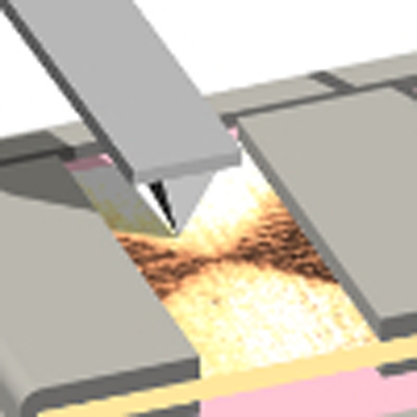 Flux-closure patterns are rarely observed in ferroelectric materials and almost exclusively form at the nanoscale. McQuaid et al. report mesoscopic dipole closure patterns formed in free-standing single-crystal lamellae of BaTiO3, thought to result from an unusual set of experimental conditions.
Although commonplace and well understood in ferromagnets, the existence of vortex domains1,2 in ferroelectrics is much less well established, despite being predicted for some time by Bellaiche and co-workers3,4. Even the quadrant closure domains predicted by Kittel5, considered as a precursor for the true vortex state, have been rarely experimentally observed in ferroelectric systems (Schilling et al. have seen distinct quadrant bundles of domains in nanodots, but detailed consideration of dipole patterns imply that flux-closure polar states are unlikely6).
Nevertheless, some key discoveries have very recently been made that start to shed light on the prevalence and stability of ferroelectric dipole closure objects: small-scale flux-closure states in BiFeO3 can be formed by direct writing using scanning probe tips7; similar closure-quadrupole chains of dipole arrangements can also form naturally at the junctions between different bundles, or packets, of domains in single-crystal BaTiO3 (ref. 8); patterns involving continuous rotation of the dipole vector, which is a prerequisite for genuine dipole vortex states to exist, can be seen directly using Aberration Corrected Transmission Electron Microscopy (Cs-TEM)9,10. Importantly, polarization closure by dipole rotation is associated with the presence of electrically non-compensating surfaces10. These observations clearly highlight the role of depolarizing fields, analogous to the demagnetizing fields that drive magnetic vortex formation. Overall though, the ferroelectrics research community has had to work hard to catch glimpses of flux-closure and vortex behaviour. For some reason, ferroelectric closure states are less obvious than ferromagnetic analogues11,12,13, suggesting that the physics associated with their existence is somewhat more subtle.
In this work, we present a set of distinct observations that shows that relatively large-scale ferroelectric closure states can readily form under the right circumstances: in particular, we note that such states do not form spontaneously on cooling through the Curie temperature; rather, their genesis is linked to domain relaxation after the application, and subsequent removal, of a uniform poling electrical field. The properties of the electron-beam deposited Platinum (Pt) electrodes, used in this work, are thought to be important due to their relatively low conductivity and, consequently, poor electrical screening of polarization. The fact that the closure structure is composed of 4 quadrants of 90° shape-conserving domains is also thought to be critical, as this allows the disclination stresses that are necessarily associated with a Kittel closure arrangement in ferroelectrics (where spontaneous polarization is strictly coupled to significant spontaneous strain) to be avoided. Because such stresses increase as the size of the quadrant closure set increases, it is likely that the stripe domains are central in explaining the obvious meso-scale nature of our observations. A similar argument could be used in discussing the structures seen by Ivry et al.14
Results
Imaging switching in single-crystal lamellae
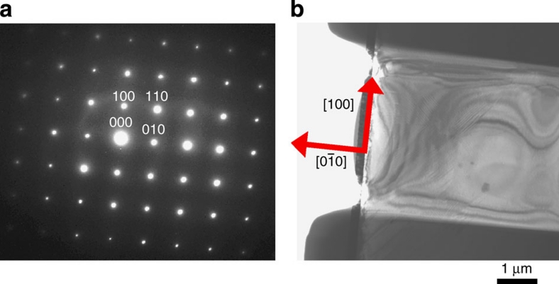
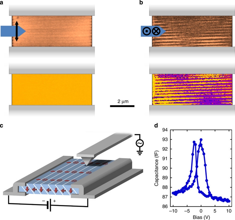
(100)pseudocubic (pc)-oriented thin slices of BaTiO3 (lamellae) were machined from a commercially obtained bulk BaTiO3 single crystal, using an established Focused Ion Beam (FIB) milling methodology15,16. Confirmation of lamellar crystallographic orientation is presented in Figure 1 and discussed in the 'Methods' section below. Lamellae were placed such that they bridged a pre-patterned interelectrode gap between Pt coplanar electrodes, deposited onto an MgO substrate, and were secured in place by localized electron-beam-induced platinum deposition (Figs 2a,b).  100
100 pc directions were such that they were parallel and perpendicular to the electrode–ferroelectric interfaces. This geometry enabled reliable interpretation of the domain states within the interelectrode gap obtained via Piezoresponse Force Microscopy (PFM) imaging17. PFM of a typical virgin domain configuration (resulting from cooling through the Curie temperature without any application of electric field) is shown in Figure 2c. Dark lines in the PFM amplitude image are boundaries between packets, or bundles, of 90° stripe domains. Overall, the domain packet distribution looks to be relatively disordered.
Figure 1. Electron Diffraction of BaTiO3 lamella.
Electron diffraction pattern (a) associated with the real space bright field transmission electron microscopy image (b). As can be seen, the sidewall and top / bottom surfaces of the lamella are all {100}pc in nature. This orientation information allows the stripe domains observed to be assigned as either 'a1-a2' or 'a-c', depending on the observed orientation of the domain walls with respect to the lamellar surfaces.
Figure 2. Experimental setup for imaging switching in BaTiO3.
(a) Schematic representation of the coplanar switching geometry with suspended BaTiO3 lamella on platinized MgO carrier with FIB patterned electrodes; the PFM cantilever is also illustrated. A DC switching voltage is supplied through wire bonds while PFM is performed in the interelectrode gap to enable imaging of the switched domain states. (b) Scanning electron microscope image of the real sample structure. The image has been colour coded to match the schematic in (a). (c) VPFM amplitude (top) and phase (bottom) images of the virgin state of the BaTiO3 lamella observed between the Pt electrodes (illustrated schematically).
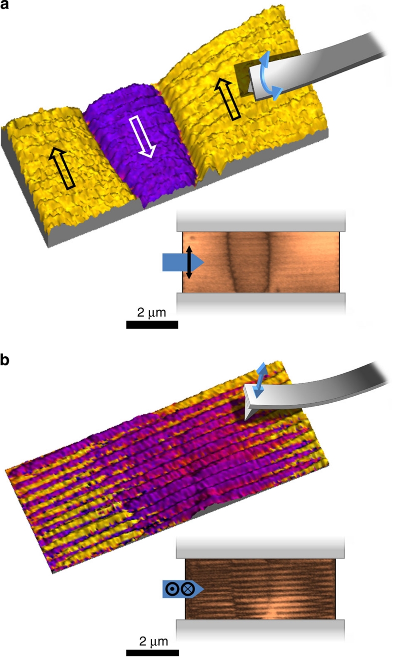
Lateral PFM (LPFM) images of the polarization state recorded immediately after planar switching (using 10VDC applied for ~2 min) are shown in Figure 3a. Capacitance-voltage (CV) data, presented in Figure 3d, indicate that the sample is likely to be fully switched under this applied bias voltage. The fully switched state seems consistent with the PFM phase information (Fig. 3a) in which a simple monodomain state is implied, with an in-plane polar vector oriented perpendicular to the electrodes (parallel to the switching field). However, there is feint horizontal stripe contrast in the LPFM amplitude. Vertical PFM (VPFM) contrast (Fig. 3b) resolves these stripe features more strongly: here, it can be seen that alternate stripes have a positive PFM phase. Combining the LPFM and VPFM information, it appears that the 'fully switched' state is composed of highly ordered a–c stripe domains in which alternate polarization vectors lie in-plane, parallel to the applied switching field (a-domains), and out-of-plane, perpendicular to the lamellar surface (c-domains). This a–c-domain structure is such that the trace of the domain walls on the exposed surface of the BaTiO3 is aligned parallel to the electrode edges ( 100
100 pc). However, the plane of these domain walls ({110}pc) slopes through the lamella thickness at 45° to the top surface. The relative dipole and domain wall orientations of these stripes are schematically illustrated in Figure 3c.
Figure 3. Domain configuration in the fully switched state.
(a) LPFM and (b) VPFM amplitude (top) and phase (bottom) images of a fully switched domain configuration. Whereas the LPFM images indicate that the in-plane component is co-aligned with the applied field direction (perpendicular to the electrodes), the VPFM data reveal an a-c-domain structure consisting of 90° stripe domains. Schematics of cantilevers are included illustrating the detected polarization components in each mode. (c) A schematic representation of the a-c-domain structure between the electrodes, also illustrating relative scan orientation of the cantilever. (d) Measured CV switching profile obtained via global switching through the coplanar electrodes (averaged over 10 cycles).
When the switching field has been removed, the domain structure in the BaTiO3 begins to relax away from the fully poled state shown in Figure 3c. Initially, the stripe domain contrast parallel to the electrodes is maintained and backswitching is mediated by the nucleation and growth of a central packet of a–c-domains (occurring over a period of minutes) in which the in-plane a-domain component has reversed in orientation. This is picked up strongly by the combined LPFM amplitude and phase images shown in Figure 4a. Clearly, a central band with opposite in-plane phase has developed (it can also be seen in the VPFM images in Figure 4b, but the contrast is more subtle). In this initial phase of backswitching, boundaries between a–c-domain packets now typically extend between electrodes and are approximately perpendicular to the electrode-ferroelectric interface. Although, in detail, the regions displaying uniform phase contrast (henceforth referred to as 'blocks') shown in Figure 4a are clearly still composed of a–c stripe domains, they are behaving very like the 180° superdomains noted previously by McGilly et al.18
Figure 4. Domain configuration in partially switched states.
Isomeric representation of (a) LPFM and (b) VPFM amplitude images with phase information overlaid. Schematic cantilevers are included illustrating the nature of the cantilever contortion associated with in- and out-of-plane polarization detection: the cantilever torsional twist in (a) registers an in-plane polarization while the vertical deflection in (b) registers an out-of-plane polarization component. The original 2D PFM amplitude images are included below. At first glance (a) implies a simple 180° domain arrangement (hollow arrows indicate relative in-plane polar orientations). However (b) clearly reveals parent a-c-domain stripe structure.
Formation of flux-closure domains
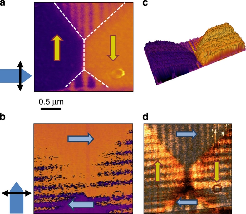
Whereas backswitching initially involved the creation of domain packets in which the in-plane domains were oriented at 180° to those in the fully switched state, given extended time (of the order of hours), triangular domain structures develop adjacent to the electrodes, which eventually create a quadrant set of domain packets. Determination of the directions of the dipoles within this more completely relaxed structure has been established using a vector PFM approach19 (Fig. 5a,b). During these measurements, the orientation between the sample and the axis of the PFM cantilever was varied to allow the in-plane components of polarization to be unequivocally assigned. Figure 5c shows a three-dimensional rendition of combined LPFM amplitude and phase images of this structure, illustrating that the solid block regions of single phase dominate the amplitude signal; we thus rely on this phase information for allocation of in-plane polar orientations to each quadrant. Clearly the quadrant structure demonstrates in-plane flux-closure (Fig. 5d). Taking note of the detectable polarization components in LPFM and the assigned in-plane polarization directions for each quadrant using the block regions of uniform phase, no stripe contrast is anticipated (that is, zero amplitude ideally) in this mode of imaging (Fig. 5a,b). We, therefore, suspect that the observed low-amplitude stripe contrast (Fig. 5c) must originate from lamella miscut and/or minor relative misrotation of the cantilever (that is, cantilever not exactly parallel to  100
100 pc type direction). For more details, see Supplementary Figures S1 and S2 and Supplementary Methods.
Figure 5. Vector PFM mapping of flux-closure domain topology.
LPFM images of the quadrant domain structure for two orthogonal cantilever orientations, (a) and (b). The dashed line in (a) tracks the boundary between the quadrants and the arrows denote relative in-plane polarization component orientation of the labelled domains. (c) An isomeric representation of the LPFM amplitude map with phase overlay (Fig 5a), indicating that the regions of uniform phase contrast (block regions) dominate in the amplitude signal over the striped regions. The block regions are therefore used for allocating polar vectors. The origin of the small-signal amplitude stripes is discussed in Supplementary Methods. (d) Parent stripe structure of the quadrants is revealed by overlaying various amplitude images which display the stripes from opposing quadrants.
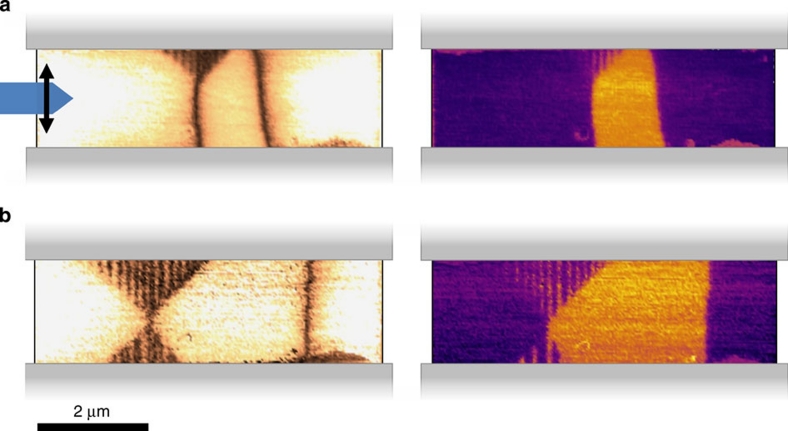
We note that the development of the flux-closed state is particularly stable but can take considerable time to fully develop. Often, after external field removal, a partially formed state is observed where only one triangular region of a–c stripe subdomains appears, but it subsequently evolves into the full-flux-closure quadrant structure over a period of up to several hours (Fig. 6).
Figure 6. Development and stabilization of flux closure domains.
(a) LPFM amplitude (left) and phase (right) images minutes after field removal showing a partially formed quadrant structure (for the boundary on the left). (b) LPFM amplitude (left) and phase (right) several hours later showing the fully formed quadrant structure.
Discussion
There are two issues related to the formation of this flux-closure structure that merit particular discussion. Firstly, that a flux-closing domain geometry (that minimizes depolarizing fields) forms in a system where mobile screening charges should be available, via the electrodes, seems counter-intuitive. Secondly, this relatively large-scale flux-closure object forms consistently on relaxation after switching in several samples; its presence is obvious and clearly related to quadrant flux-closure. Yet, prior investigations seeking closure or vortex states in ferroelectrics have had to rely on direct writing of topological defects20, on pre-established microstructure14, or on rather subtle inferences made from experimental data21,22. Why are the flux-closure quadrant structures observed here so obvious and yet in previous work they have been so difficult to find?
With regards to the first point, we note that the electron-beam deposited electrodes used in our work have a resistivity reported to be six orders of magnitude higher than pure bulk platinum23. We suggest that these electrodes, while allowing the application of a switching voltage to the BaTiO3, are insufficiently conducting to provide effective charge compensation after the voltage has been removed. Depolarizing fields can therefore develop, prompting domain reorientation/redistribution. With regards to the second issue, we believe that the interior stripe domain structure within each quadrant in the flux-closure object in our work is vital for stabilizing the structure against disclination stresses that are expected to develop at the quadrant boundaries. Without these shape-conserving domains, flux-closure states should be subject to hoop stresses, the magnitude of which increases with the physical size of the flux-closure objects6. Although the almost free-standing geometry investigated here clearly allows 90°-shape-conserving domains to form, this is not the case in most experimental investigations. This crucial requirement of a stress-relieving ferroelastic striped domain structure is highlighted in a simple calculation by Catalan et al.24. They show that, for such a quadrant configuration to extend beyond a few nanometers in size, internal elastic stresses make it energetically more feasible to introduce additional domain walls; additionally, detailed ab initio25,26 and first principle calculations27 in ultrathin ferroelectric perovskite films suggest that flux-closure type domains can only be stabilized on scales of a few unit cells. This critical size correlates with the experimental observation of Jia et al., that is, of a flux-closing dipole arrangement (with no internal stripe domain structure) being supported on the scale of a few nanometers9.
We note that the time evolution of the quadrant structure presented in Figures 5 and 6 can be described by the preferential stabilization of specific vertex patterns (junctions between two or more domain walls) identified in a Clock-model description, previously reported by Srolovitz and Scott28. Remarkably, development of the flux-closure object occurs on the timescales of hours, suggesting vertex velocities comparable with those measured in relaxation and faceting of written 180° nanodomains in PbZr0.2Ti0.8O3 (refs 29,30); this wall motion has been rationalized as a creep process30,31 and is a possible mechanism for describing the growth dynamics associated with the flux-closure vertices in the present study, with the residual depolarizing field acting as the driving force for the evolution of this pseudo-equilibrium structure.
In summary, we have used vector PFM analysis to map the nature of mesoscopic flux-closure domain patterns that form spontaneously in single-crystalline BaTiO3 lamellae after removal of a uniform applied poling field. We suggest that the observed mesoscale flux-closure quadrant domains result from a particular combination of experimental conditions: first, it involves relaxation from an initial fully poled state (the closure quadrant states do not form spontaneously on cooling through the Curie temperature); second, the poor conductivity of the electron-beam deposited Pt results in incomplete polarization screening and therefore in significant depolarizing fields; finally, compensation of disclination stresses, normally associated with flux-closure in ferroelectrics, has been mediated by the existence of shape-conserving stripe domain sets.
Methods
Sample preparation
(100)pc-oriented thin single-crystal BaTiO3 lamellar slices (~300 nm in thickness) were machined from commercially obtained polished bulk single crystals using a single beam FEI200TEM FIB. Lamellae were completely cut free from the host crystal and removed using a micromanipulator-controlled fine glass needle. The lamella could therefore be carefully balanced across the 2 μm interelectrode gap of a (sputter-coated) platinized passive MgO carrier having a prior FIB-etched coplanar electrode structure. Similar coplanar type capacitor geometries have previously been employed for explicit PFM imaging of ferroelectric switching: for example, those employed in refs 32, 33, 34 (finite element modelling of the spatial electric field distribution across a 1 μm interelectrode gap by You et al.34 shows some field inhomogeneity at the ferroelectric/electrode interface, but note that the field distribution is otherwise almost uniform through the ferroelectric). The structure was annealed at 700 °C in air to fully re-crystallize the lamella after FIB-induced surface damage, and to expel gallium ion contamination, as described in ref. 35. Etching in 3 M HCl solution for several minutes was found to be sufficient to remove the gallium oxide islands that form on the surface, leaving a smooth pristine surface suitable for PFM investigation. The lamella is then fixed in place either side of the interelectrode gap by in-situ electron-beam-induced deposition of platinum (using a FEI Nova 600 DualBeam system); this ensures electrical contact with the FIB patterned electrodes. Here the electron beam is used to induce local dissociation of a precursor gas (MeCpPtMe3) to deposit metal at the target location while leaving the remaining volatile fragments to be evacuated out of the system. Finally, wire-bond connections were made between the FIBed electrode pads and an external macroscopic electrode structure allowing electric field application to the sample while placed in an Atomic Force Microscope system. CV hysteresis loops (Fig. 3d) were measured through the coplanar electrode structure using a HP4192A impedance analyser.
Electron diffraction confirmation of lamella crystallography
Interpretation of the domain contrast, and the inferred local polarization vectors, rely on the crystallographic orientation of the BaTiO3 lamella being known. Figure 1 shows an electron diffraction pattern and a TEM image of a lamella that has been cut in the same orientation as those that were integrated into the coplanar electrode capacitor structures and imaged for the present study. The central region has been further thinned to allow electron transparency and electron diffraction patterns to be obtained. The electron diffraction pattern shows the 100-type reflections to be parallel and perpendicular to the sidewalls of the lamella. The zone axis is also of  100
100 type, such that 100 reciprocal lattice reflections would also be perpendicular to the lamellar surface. Thus, all the bounding surfaces of the lamella are approximately {100} faces.
PFM domain imaging
PFM measurements were performed jointly between systems at both Queen's University Belfast (QUB) and the University of Nebraska-Lincoln (UNL). PFM data displayed in Figures 2,3,4 were obtained at QUB while those in Figures 5 and 6 were obtained at UNL. In both cases the cantilever axis was aligned parallel to the electrode edges and measurements were performed in an ambient air environment. The QUB system comprised of a Veeco Dimension 3100 AFM system with a Nanoscope IIIa controller modified for PFM measurements, using a EG&G 7265 lock-in-amplifier. Here a probing signal of 1.5 Vrms at a frequency of 20kHz was applied to a Nanosensors PPP–EFM cantilever (force constant ~2.8 N/m). Measurements at UNL were performed using a commercial Asylum Research MFP-3D system. The same tips were used as above with a 1.5 Vpp probe signal but operated near contact resonance, for lateral and vertical modes, respectively, to enhance the signal-to-noise ratio (670–675 kHz in LPFM mode and 330–335 kHz in VPFM mode). For unambiguous mapping of polarization, in complex domain configurations, 3D vector PFM imaging was performed by collecting a vertical piezoresponse component and two lateral piezoresponse components19. In the latter case, the sample was rotated by 90° to discriminate between orthogonally oriented in-plane polar vector components. The lamella was switched by biasing the planar electrodes (up to 10 VDC) and PFM measurement was performed in the interelectrode gap by AC biasing the scanning PFM probe. In all figures the domain configurations presented are remnant configurations, visualized after the removal of the poling field.
Author contributions
R.G.P.McQ., A.G. and J.M.G. conceived and designed the experiments. R.G.P.McQ. prepared samples, both for PFM and TEM investigations, and performed the electrical characterization. R.G.P.McQ., L.J.McG. and P.S. performed PFM measurements. J.M.G. performed TEM and rationalized electron diffraction information. R.G.P.McQ. and J.M.G. primarily wrote the manuscript. All authors contributed to data analysis and commented on the manuscript.
Additional information
How to cite this article: McQuaid, R. G. P. et al. Mesoscale flux-closure domain formation in single crystal BaTiO3. Nat. Commun. 2:404 doi: 10.1038/ncomms1413 (2011).
Supplementary Material
Supplementary Figures S1-S2 and Supplementary Methods.
Acknowledgments
The authors acknowledge financial support from the Engineering and Physical Sciences Research Council (EPSRC) and the National Science Foundation (NSF) for funding under the Materials World Network (MWN) scheme (NSF Grant No.: DMR-1007943; EPSRC Grant No.: EP/H047093/1), and The Leverhulme Trust for international network funding (F/00 203/V). R.G.P.McQ., L.J.McG. and J.M.G. acknowledge support from the Department of Employment and Learning (DEL). R.G.P.McQ. acknowledges support from the Dunville Studentship scheme. P.S. and A.G. acknowledge support from the NSF under Grant No. MRSEC DMR-0820521.
References
- Shinjo T., Okuno T., Hassdorf R., Shigeto K. & Ono T. Magnetic vortex core observation in circular dots of permalloy. Science 289, 930–932 (2000). [DOI] [PubMed] [Google Scholar]
- Wachowiak A. et al. Direct observation of internal spin structure of magnetic vortex cores. Science 298, 577–580 (2002). [DOI] [PubMed] [Google Scholar]
- Naumov I. I., Bellaiche L. & Fu H. Unusual phase transitions in ferroelectric nanodisks and nanorods. Nature 432, 737–740 (2004). [DOI] [PubMed] [Google Scholar]
- Fu H. & Bellaiche L. Ferroelectricity in barium titanate quantum dots and wires. Phys. Rev. Lett. 91, 257601 (2003). [DOI] [PubMed] [Google Scholar]
- Kittel C. Theory of the structure of ferromagnetic domains in films and small particles. Phys. Rev. 70, 965–971 (1946). [Google Scholar]
- Schilling A. et al. Domains in ferroelectric nanodots. Nano Lett. 9, 3359–3364 (2009). [DOI] [PubMed] [Google Scholar]
- Balke N. et al. Deterministic control of ferroelastic switching in multiferroic materials. Nat. Nano. 4, 868–875 (2009). [DOI] [PubMed] [Google Scholar]
- McGilly L. J., Schilling A. & Gregg J. M. Domain bundle boundaries in single crystal BaTiO3 lamellae: searching for naturally forming dipole flux-closure/quadrupole chains. Nano Lett. 10, 4200–4205 (2010). [DOI] [PubMed] [Google Scholar]
- Jia C.- L., Urban K. W., Alexe M., Hesse D. & Vrejoiu I. Direct observation of continuous electric dipole rotation in flux-closure domains in ferroelectric Pb(Zr,Ti)O3. Science 331, 1420–1423 (2011). [DOI] [PubMed] [Google Scholar]
- Nelson C. T. et al. Spontaneous vortex nanodomain arrays at ferroelectric heterointerfaces. Nano Lett. 11, 828–834 (2011). [DOI] [PubMed] [Google Scholar]
- Ozdemir O., Xu S. & Dunlop D. J. Closure domains in magnetite. J. Geophys. Res. 100, 2193–2209 (1995). [Google Scholar]
- Runge K. et al. High-resolution observation of magnetization processes in 2×2×0.04 μm permalloy particles. J. Appl. Phys. 79, 5075–5077 (1996). [Google Scholar]
- Jubert P.- O., Toussaint J.- C., Fruchart O., Meyer C. & Samson Y. Flux-closure-domain states and demagnetizing energy determination in sub-micron size magnetic dots. Europhys. Lett. 63, 132–138 (2003). [Google Scholar]
- Ivry Y., Chu D. P., Scott J. F. & Durkan C. Flux closure vortexlike domain structures in ferroelectric thin films. Phys. Rev. Lett. 104, 207602 (2010). [DOI] [PubMed] [Google Scholar]
- Chang L.- W., McMillen M., Morrison F. D., Scott J. F. & Gregg J. M. Size effects on thin film ferroelectrics: experiments on isolated single crystal sheets. App. Phys. Lett. 93, 132904 (2008). [Google Scholar]
- McQuaid R. G. P., Chang L.- W. & Gregg J. M. The effects of antinotches on domain wall mobility in single crystal ferroelectric nanowires. Nano Lett. 10, 3566–3571 (2010). [DOI] [PubMed] [Google Scholar]
- Gruverman A. & Kalinin S. V. Piezoresponse force microscopy and recent advances in nanoscale studies of ferroelectrics. J. Mater. Sci. 41, 107–116 (2006). [Google Scholar]
- McGilly L. J. & Gregg J. M. Scaling of superdomain bands in ferroelectric dots. App. Phys. Lett. 98, 132902 (2011). [Google Scholar]
- Kalinin S. V. et al. Vector piezoresponse force microscopy. Microsc. Microanal. 12, 206–220 (2006). [DOI] [PubMed] [Google Scholar]
- Vasudevan R. K. et al. Exploring topological defects in epitaxial BiFeO3 thin films. ACS Nano 5, 879–887 (2011). [DOI] [PubMed] [Google Scholar]
- Gruverman A. et al. Vortex ferroelectric domains. J. Phys. Condens. Matter. 20, 342201 (2008). [Google Scholar]
- Rodriguez B. J. et al. Vortex polarization states in nanoscale ferroelectric arrays. Nano Lett. 9, 1127 (2009). [DOI] [PubMed] [Google Scholar]
- Botman A., Mulders J. J. L., Weemaes R. & Mentink S. Purification of platinum and gold structures after electron-beam-induced deposition. Nanotechnology 17, 3779–3785 (2006). [Google Scholar]
- Catalan G., Seidel J., Ramesh R. & Scott J. F. Domain wall nanoelectronics. Rev. Mod. Phys. in press (2011). [Google Scholar]
- Aguado-Puente P. & Junquera J. Ferromagneticlike closure domains in ferroelectric ultrathin films: first-principles simulations. Phys. Rev. Lett. 100, 177601 (2008). [DOI] [PubMed] [Google Scholar]
- Shimada T., Tomoda S. & Kitamura T. Ab initio study of ferroelectric closure domains in ultrathin PbTiO3 films. Phys. Rev. B 81, 144116 (2010). [Google Scholar]
- Kornev I., Fu H. & Bellaiche L. Ultrathin Films of Ferroelectric Solid Solutions under a Residual Depolarizing Field. Phys. Rev. Lett. 93, 196104 (2004). [DOI] [PubMed] [Google Scholar]
- Srolovitz D. J. & Scott J. F. Clock-model description of incommensurate ferroelectric films and of nematic-liquid-crystal films. Phys. Rev. B 34, 1815–1818 (1986). [DOI] [PubMed] [Google Scholar]
- Ganpule C. S. et al. Polarization relaxation kinetics and 180° domain wall dynamics in ferroelectric thin films. Phys. Rev. B 65, 014101 (2001). [Google Scholar]
- Scott J. F., Gruverman A., Wu D., Vrejoiu I. & Alexe M. Nanodomain faceting in ferroelectrics. J. Phys. Condens. Matter 20, 425222 (2008). [Google Scholar]
- Tybell T., Paruch P., Giamarchi T. & Triscone J.- M. Domain wall creep in epitaxial ferroelectric Pb(Zr0.2Ti0.8)O3 Thin Films. Phys. Rev. Lett. 89, 097601 (2002). [DOI] [PubMed] [Google Scholar]
- Shafer P., Zavaliche F., Chu Y. H., Yang P. L., Cruz M. P. & Ramesh R. Planar electrode piezoelectric force microscopy to study electric polarization switching in BiFeO3. Appl. Phys. Lett. 90, 202909 (2007). [Google Scholar]
- Balke N. et al. Direct observation of capacitor switching using planar electrodes. Adv. Funct. Mater. 20, 3466–3475 (2010). [Google Scholar]
- You L. et al. Polarization switching in quasiplanar BiFeO3 capacitors. App. Phys. Lett. 97, 062910 (2010). [Google Scholar]
- Schilling A., Adams T., Bowman R. M. & Gregg J. M. Strategies for gallium removal after focused ion beam patterning of ferroelectric oxide nanostructures. Nanotechnology 18, 035301 (2007). [DOI] [PubMed] [Google Scholar]
Associated Data
This section collects any data citations, data availability statements, or supplementary materials included in this article.
Supplementary Materials
Supplementary Figures S1-S2 and Supplementary Methods.


