Abstract
We present a procedure for forming a poly(ethylene glycol) (PEG) trimethoxysilane self-assembled monolayer (SAM) on a silicon substrate with gold microelectrodes. The PEG-SAM is formed in a single assembly step and prevents biofouling on silicon and gold surfaces. The SAM is used to coat microelectrodes patterned with standard, positive-tone lithography. Using the microtubule as an example, we apply a DC voltage to induce electrophoretic migration to the SAM-coated electrode in a reversible manner. A flow chamber is used for imaging the electrophoretic migration and microtubule patterning in situ using epifluorescence microscopy. This method is generally applicable to biomolecule patterning, as it employs electrophoresis to immobilize target molecules and thus does not require specific molecular interactions. Further, it avoids problems encountered when attempting to pattern the SAM molecules directly using lithographic techniques. The compatibility with electron beam lithography allows this method to be used to pattern biomolecules at the nanoscale.
Protocol
Preparation of reagents
Prepare PIPES buffer (80 mM PIPES, 1mM MgCl2, 1mM EGTA, adjusted to pH 6.8 with KOH). Aliquot and store glucose oxidase, catalase and glucose at -70°C and taxol at -20°C according to existing protocols.1,2 Aliquot and store tubulin at -70°C according to the instructions included by the supplier.
Pattern Au microelectrodes using lithography
Cut silicon wafers into 1 cm ´ 1.5 cm substrates using a scribe or wafer cutter. Clean the substrates by placing them in a beaker with enough acetone to cover them and sonicate for 5 minutes. Without allowing the substrates to dry, rinse them in fresh acetone, then immediately rinse in isopropanol and dry using nitrogen.
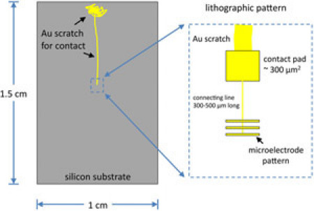
Fabricate Au microelectrodes on the clean substrates using standard, positive-tone photolithography or electron beam lithography, depending on the size of the features desired.3 When designing the pattern geometry, keep the diameter of each electrode pattern below 100 microns to ensure coverage by the PEG SAM (described in the next section). Include contact pads (~ 300 mm 2) positioned 300 to 500 mm from the pattern with a 1 mm line connecting the pad with the electrode (Fig. 1). Place the lithographic patterns near the middle of the substrate to allow space around the pattern for assembling the flow chamber.
 Figure 1. Sample geometry. Please click here to see a larger version of figure 1.
After development of the pattern in the resist layer, scratch a line in the resist from the contact pad to the edge of the substrate using tweezers (Fig. 1). Upon metal deposition, the scratch will allow electrical contact between the electrode and the edge of the substrate. A deposition chamber, preferably with two sources, is used to deposit the metal layer. The electrodes are formed by deposition of 2 nm of Cr (for adhesion) followed by 6 nm of Au, without breaking vacuum. A quartz crystal microbalance equipped inside the chamber can be used to measure the thickness of the films during deposition.
Prepare the SAM
Preheat and oven in a well-ventilated area to 75°C. Prepare the silanization solution by adding 20 mL of toluene to a 250 mL glass beaker. Then add 1 mL PEG-silane (i.e. 5% v/v) to the toluene using a plastic pipette. Mix in the PEG-silane well by pipetting up and down 5 to 10 times and then stirring with the pipette for 30 seconds.
Place the patterned samples in the beaker with the patterned side facing upwards, making sure that they are completely submerged in the PEG-silane toluene solution and are evenly spaced across the bottom of the beaker. Place the beaker in the oven and bake 18 to 21 hours at 75°C. While the SAM is forming, prepare the counterelectrode (see below) and assemble any additional components required for the remaining steps.
After 18-21 hours in the oven, the toluene should evaporate leaving the patterned samples in a viscous PEG-silane residue. Add 20 mL of toluene to the beaker and soak the samples for 1-2 minutes. Remove the samples from the beaker and rinse with toluene, then isopropanol, and finally dry with nitrogen. At this point, the samples should look clean and the SAM layer should be invisible to the naked eye. SAMs prepared this way are usable for up to two days when stored under cool dry conditions (25 °C, moderate humidity). Unsuccessful SAM formation results in a cloudy or uneven hued residue coating on the surface.
Fabricate the counterelectrode
In the same deposition chamber setup used for microelectrode deposition, make a counterelectrode by depositing 1 nm of Cr, followed by 4 nm of Au onto a 22 x 50 mm No. 1 or No. 0 glass coverslip. The counterelectrode should be nearly transparent with a light gray or pink tint. Store the counterelectrode coated-side-up in a Petri dish to keep it clean.
Polymerize tubulin into MTs
Thaw unlabeled tubulin and rhodamine tubulin and immediately combine at a ratio of 1:2 labeled to unlabeled to obtain bright MTs. Mix by pipetting up and down several times. Polymerize the tubulin for 20-40 minutes in a heated water bath at 37°C. The length of the MTs will be greater for longer polymerization times. While the tubulin is polymerizing, prepare a PIPES-taxol buffer by adding taxol to 20 mM into a microcentrifuge tube containing PIPES buffer. Mix the taxol well by pipetting up and down several times and vortexing, and then place the tube into the heated bath at 37°C. After polymerization, dilute the MTs by 1/100 in warm PIPES-taxol buffer and shield from light. MTs prepared in this way will elongate over time and bundle, which can be reduced by further dilution.
Prepare a 10x oxygen scavenging mixture (OS) by combining 30 mL cold PIPES buffer (0-4°C), 5 mL of 50% 2-mercaptoethanol, 5 mL glucose oxidase, 5 mL catalase, and 5 mL glucose.2 The glucose should be added last. Mix by pipetting up and down 3-5 times after adding each component. Place the OS mixture on ice; it will remain effective for about 2 hours.
Verify that the MT polymerization was successful and that the MTs are stable under several minutes of fluorescence excitation by imaging the prepared MTs with 1x OS mix. For imaging the MTs prepared in this way, be sure to use an excitation/emission filter combination suitable for rhodamine fluorescence. Determine the best working dilution for imaging individual filaments by further diluting the MTs by 1/10 to 1/100 using PIPES buffer and imaging with 1x OS mix.
Prepare a flow chamber by sandwiching a large (22 x 50 mm) and small (22 x 22 mm) glass coverslip with two pieces of double-sided tape placed 2-3 mm apart. The tape is easily cut into strips by placing it on a glass slide and cutting with a razor blade. Introduce a few microliters of MTs into the flow cell using a micropipette. For high magnification imaging, long working distance objectives may be required for imaging the upper surface of the flow chamber. The distance from the coverslip/sample surface to the upper surface of the flow chamber is determined by the thickness of the tape and should be 60-100 mm.
Pattern MTs using electrophoresis
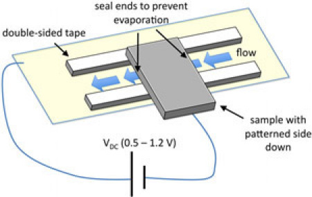
Prepare an electrophoresis chamber by placing two thin strips of double-sided tape across the patterned, SAM-coated sample such that the electrode is between the strips with the connecting path running perpendicular to the tape (Fig. 2). Place the counterelectrode on the double-sided tape with the metal side touching the tape such that the edge of the sample overhangs the counterelectrode by about 3 mm (Fig. 2). Cut several 15 cm lengths of the insulated copper magnet wire and strip 1 cm of the insulation off of both ends. Attach a wire to the exposed Au area of the substrate using a small drop of silver paint while taking care to avoid making electrical contact with the counterelectrode (this can be checked with a multimeter). Attach a second wire to the counterelectrode using silver paint. Wires attached with silver paint can be further secured to the samples with tape.
 Figure 2. Flow cell assembly for an inverted fluorescence microscope. Please click here to see a larger version of figure 2.
Introduce MTs at the desired dilution using PIPES buffer combined with OS at 1x final concentration. Image at 20X magnification and locate the pattern on the silicon wafer before applying a voltage. Optionally, the flow chamber can be sealed using nail polish to prevent fluid flow and MT migration in the plane of the flow chamber.
Apply a voltage up to 1 V and observe migration of MTs. Lower voltages (down to about 0.5 V) may be used if reversible trapping of MTs is desired; however this requires sealing the flow chamber to prevent lateral drift. Nail polish works well for sealing the open ends of the flow chamber. At voltages above about 0.7 V, some MT adhesion may be seen on the pattern, though it will be weak. At voltages above about 0.9 V, the MT migration will be faster, and the adhesion will be stronger. Above about 1.2 V the likelihood for inducing electrolysis (gas bubble formation) and also for destroying the microelectrodes increases significantly. Migration can be tracked by adjusting the vertical plane of focus of the microscope. If carried out correctly, the MTs will localize at the electrode surfaces.
Discussion
The migration of MTs is easily visualized using fluorescence microscopy because of their brightness and the low background fluorescence. The method is generally applicable to biomolecule patterning, as it only requires that the biomolecules be induced to carry a net charge by suitable adjustment of the buffer pH. Electroosmosis is avoided in this setup because there are no charged surfaces such as the silica walls used in capillary electrophoresis.
Several modifications of this method are possible. Sealing the ends of the flow chamber is critical to observe reversibility because evaporation from the open ends causes bulk fluid flow and undesirable MT migration. Oxidation of the silicon wafer prior to lithographic patterning will prevent conduction through the substrate, allowing for multiple electrodes with independent potentials to be used simultaneously.
Acknowledgments
We acknowledge Melissa Grunlan for helpful discussions on SAM formation. This research was supported in part by the Robert A. Welch Foundation (A-1585).
References
- Tubulin Polymerization with GTP/GMPCPP/Taxol [Internet] Cambridge, Ma: Harvard University; 2009. Available from: http://mitchison.med.harvard.edu/protocols/poly.html. [Google Scholar]
- Flow Cell Assays with Microtubules: Motility/Dynamics [Internet] Cambridge, Ma: Harvard University; 2009. Available from: http://mitchison.med.harvard.edu/protocols/flowcell.html. [Google Scholar]
- Rai-Choudhury P, editor. Handbook of Microlithography, Micromachining, and Microfabrication: Microlithography. Bellingham, WA: SPIE Press; 1997. [Google Scholar]


