

Abstract
High purity, single crystal CVD diamond plates are screened for quality and instrumented into a sensor assembly for quantitative characterization of flux and position sensitivity. Initial investigations have yielded encouraging results and have led to further development. Several limiting complications are observed and discussed, as well as mitigations thereof. For example, diamond quality requirements for x-ray diodes include low nitrogen impurity and crystallographic defectivity. Thin electrode windows and electronic readout performance are ultimately also critical to device performance. Promising features observed so far from prototype devices include calculable responsivity, flux linearity, position sensitivity and timing performance. Recent results from testing in high flux and high speed applications are described.
Keywords: diamond, synchrotron, responsivity, x-ray, detector, diode, high-flux, white beam, position monitor
1. Introduction
Diamond photoabsorption sensors for synchrotron radiation (SR) sources have been under development by several groups over the past decade [1]. White beam position and flux monitors are useful for commissioning and maintenance of synchrotron beams and beamlines. Features which make diamond particularly attractive for synchrotrons include its low x-ray absorption and high thermal conductivity. Using diamond in a transmission-diode configuration (bias applied to intrinsic semiconductor crystal) can provide calculable responsivity and flux linearity, as well as high-speed performance unachievable from photoconductors or ion chambers in high flux environments. Performance of such devices remains limited by material quality.
2. Specific observations to date
High-purity single-crystal chemical-vapor-deposition (SC-CVD) diamond available from Element Six does have the ultra-low (sub-ppm) nitrogen content required for use in detectors [2]. This material can be contrasted with the typically higher impurity levels of high-pressure, high-temperature (HPHT) diamond which can be grown faster and often with higher crystal quality; in that case, ppm-level nitrogen uniformity can yield a strain-free yet electrically inferior crystal [3,4]. That is, the ultra-low impurity level necessary for production of sensors with minimal charge trapping (large charge collection distance) requires the slower CVD process.
The crystal quality of such high purity SC samples however must also be taken into consideration. Crystal defects cause localized responsivity changes; for example, some which appear to be localized near the polished surfaces can cause localized charge trapping and photoconductive gain [5]. These regions are responsible for nonlinear flux response and residual current in devices made of lower quality diamond material [6]. These defects appear to predominantly trap electrons, however even when such defects are present, mitigation can sometimes be made by preparation of blocking contacts (acid preparation and/or ozone treatment prior to metallization creates an oxygen-terminated blocking layer which can survive up to ∼ 600 °C in vacuum). X-ray topographic imaging appears to be a useful method for identifying and screening diamond plates for defects which affect the responsivity of assembled detectors [5].
Under soft x-ray illumination, charge propagation is particularly challenging, since x-rays do not penetrate deeply enough into diamond plates to assist with de-trapping of charge in the bulk. In this case, pulsed biasing can be used to provide a sensor with predictable responsivity (detrapping occurs during zero-bias illumination); recovery time may be flux and photon energy dependent [7].
It should be noted that although nitrogen has been identified as a main contributor to charge trapping [8], several authors have had limited success with polycrystalline and nitrogen-containing diamond [9]. Although charge trapping has been observed for nitrogen-containing diamond, such behavior may in some cases be attributable to other contaminants [10]. Polycrystalline diamond is likewise expected to limit spatial resolution and uniformity [11] and can even lead to incomplete current-mode charge collection [12]. Most promising quantitative performance has in fact been observed from single-crystal high purity diamond plates [1].
Monochromatic beam tests have shown that for a wide range of photon energies (0.2-25 keV) the diode-like responsivity of diamond sensors is predictable, and that the mean electron-hole pair production energy is 13.3 eV; full collection of charge is reached at electric fields of 0.2 MV/m and above [7]. This allows such devices to provide absolute power measurements for sources of known energy bandwidth. A compact, robust, solid-state form of these devices is an attractive solution to flux and position monitoring for both white and monochromatic beams.
3. Recent progress in development of white beam position and flux monitor at NSLS
Tests performed in a variety of white beam environments at NSLS have helped to prove the capability of diamond diodes for high flux and high speed utilization.
The X28C (footprinting) beamline provides white or pink bending magnet (BM) radiation, at in this case up to 11 W in a 7×2 or 0.6×1 mm2 format onto the diamond plate (behind a 1.6 mm diameter steel pinhole). In the focused condition up to 85 mA has been produced, corresponding to ∼1 W absorbed power at ∼20 W/mm2 incident flux density. At this beamline, both flux linearity and GHz bandwidth have been demonstrated at high flux [13].
At the X15A (diffraction-enhanced imaging) beamline, white beam power of up to ∼200 mW is available from unfocused BM at 2 mm2 slit size (∼100 mW/mm2 flux density). Tests were performed with smaller slits in order to probe the position resolution performance of a quadrant device.
For the quadrant metallization pattern (∼20 nm Pt with ∼50 μm gap between adjacent pads) shown in Fig. 1, relative position d is determined from relative contrast using the following expressions:
Figure 1.
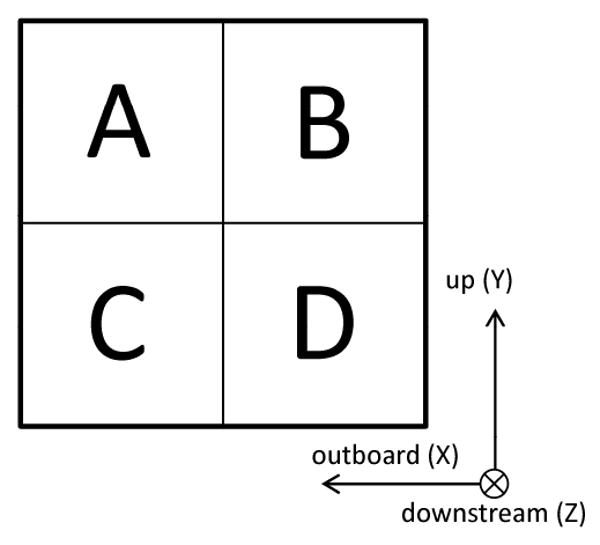
Quadrant pattern / pad arrangement used for position monitoring. For small beams, such as tested NSLS X15A, a single 4.7 mm square plate is metallized with four 2 mm square pads. For the larger beam of NSLS X25, two such plates are used, each with two 4.4 mm by 1 mm rectangular pads. Plate thicknesses used to date range from 0.1 to 0.5 mm.
dx = Gx·[[A+C]-[B+D]]/[A+B+C+D] (outboard)
dy = Gy·[[A+B]-[C+D]]/[A+B+C+D] (up)
where A,B,C and D are currents from the four pads and values G are scaling factors (“gain”) in the two dimensions. For best results, values for G are obtained experimentally; however, it is useful to note that for uniform illumination (constant flux density over a well-defined rectangular beam) and negligible gap between pads (illuminated dead area insignificant compared to illuminated metallized area), the values of G can readily be estimated as simply half the beam size (since G can be considered to have units of length per contrast). This implies that for limited relative precision in current measurements, position resolution could be limited to the product of G and this relative precision value; for example, a 2 mm beam sampled with 0.1% current accuracy might be expected to produce relative position values accurate to 1 μm. This relative limit is expected for large beams. Towards the other extreme, reduction in beam size can also reduce positioning accuracy in an absolute sense by moving measured current towards the electrical noise floor. Between these ranges, a minimum can be found where the noise is limited by parameters independent of flux and beam size, such as beam motion, stage motion, slit motion, and intrinsic resolution of the device. Initial investigations suggest this high-performance range may exist near nA-range total photocurrent, given typical readout electronics. Position resolution has been estimated for a range of slit and flux conditions at X15A by calibrating the position sensitivity (measuring G) and collecting statistics (standard deviation) for several hundred position measurements using that G over a period of a few minutes. Typical resolution (RMS noise) values we have obtained using this method so far are in the range of 30-50 nm, as illustrated in Fig. 2.
Figure 2.

Representative position / contrast calibration and noise data for NSLS-X15A white beam (∼40 × 40 μm2 of ∼100 mW/mm2 BM source).
At the X25 (macromolecular crystallography) beamline a diamond quadrant BPM was recently inserted in the white beam, downstream of the mini-gap undulator (MGU) by only slits, beryllium window and graphite filter. A total of 100 W incident power in ∼ 4 mm × 1 mm beam (25 W/mm2) generates up to 700 mA of current in the sensor, which in this case was comprised of two diamond plates tiled side-by-side to accommodate the larger beam size. The current is carried by 20 AWG copper wiring rated to 1.5 A. This photocurrent represents roughly 10% power absorption by the diamond plates, mainly from in the soft (unused) wavelengths from the source. Operating temperature of the sensor was less than 100 °C. Preliminary tests of the device illustrate a misalignment of electron beam to the undulator as a position shift of 10-20 μm horizontally of the beam center-of-mass with positioning error of 1 μm or less over the gap range (see Fig. 3). Further description of this device and its performance for high-flux white beam position and flux monitor are subjects of a more detailed article under preparation.
Figure 3.
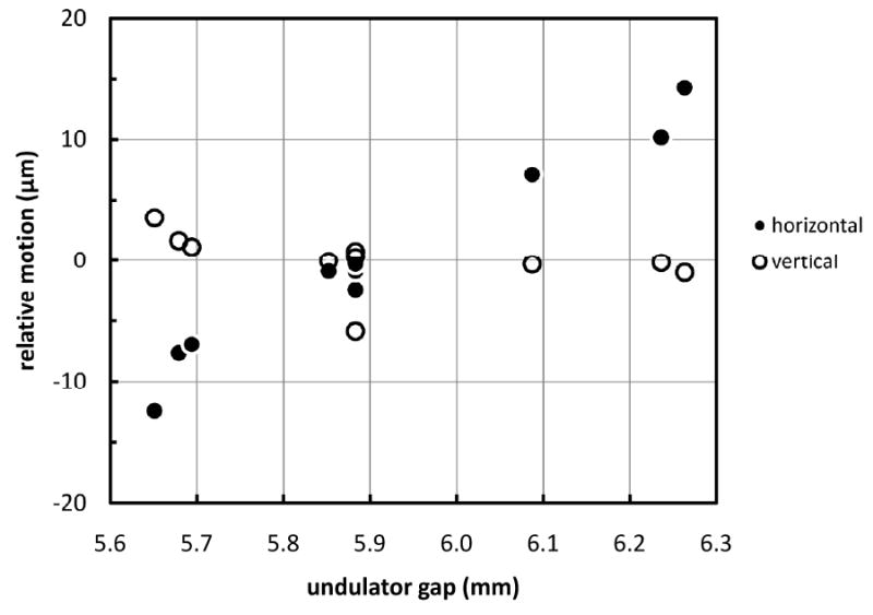
Relative position of NSLS-X25 MGU white beam center-of-mass vs. gap opening as measured by diamond white beam sensor.
4. Summary
Ultrahigh-purity single crystal CVD diamond can be used to provide a thermally stable high-flux intensity and position monitor for white and monochromatic SR beams. Current-mode measurements offer quantitative flux and position information for pseudo-continuous synchrotron x-ray beams. Crystal quality improvements are anticipated to make such devices more common and readily realizable in the coming years.
Acknowledgments
The authors wish to acknowledge NSLS and the staff of its beamlines for support of the characterization work presented here, as well as the staff of the BNL Instrumentation Division for support of device and system assembly. This work was supported in part by the U.S. Department of Energy under Grants No. DE-FG02-06ER84509 and DE-FG02-08ER41547. Use of the National Synchrotron Light Source, Brookhaven National Laboratory, was supported by the U.S. Department of Energy, Office of Science, Office of Basic Energy Sciences, under Contract No. DE-AC02-98CH10886. Use of X28C was supported by the Center for Synchrotron Biosciences under NIBIB-P30-EB-009998.
Footnotes
Publisher's Disclaimer: This is a PDF file of an unedited manuscript that has been accepted for publication. As a service to our customers we are providing this early version of the manuscript. The manuscript will undergo copyediting, typesetting, and review of the resulting proof before it is published in its final citable form. Please note that during the production process errors may be discovered which could affect the content, and all legal disclaimers that apply to the journal pertain.
References
- 1.See for example Morse J, Salomé M, Berdermann E, et al. Diamond and Related Materials. 2007;16:1049–1052.
- 2.See for example Kaneko JH, Tanaka T, Imai T, et al. NIMA. 2003;505:187–190.
- 3.Macrander A, Krasnicki S, Zhong Y, et al. Appl Phys Lett. 2005;87:194113. [Google Scholar]
- 4.Pace E, Vinattieri A, Pini A, et al. Phys Stat Sol (A) 2000;181:91. [Google Scholar]
- 5.Smedley J, Keister J, Muller E, et al. MRS Proceedings Fall 2009. 2010;1203:J17–21. [Google Scholar]
- 6.Keister J, Smedley J, Dimitrov D, et al. IEEE Trans Nucl Sci. 2010;57:2400–2404. [Google Scholar]
- 7.Keister J, Smedley J. NIMA. 2009;606:774–779. [Google Scholar]
- 8.Kania D. In: Proc Intl Sch Phys. Paoletti A, Tucciarone A, editors. Vol. 135. IOS Press; 1996. pp. 555–564. “Enrico Fermi,” The Physics of Diamond. [Google Scholar]
- 9.Bergonzo P, Tromson D, Mer C. J Synch Rad. 2006;13:151–158. doi: 10.1107/S0909049505032097. [DOI] [PubMed] [Google Scholar]
- 10.Schirru F, Kupriyanov I, Marczewska B, Nowak T. Phys Stat Sol A. 2008;205(9):2216–2220. [Google Scholar]
- 11.Bol J, Müller S, Berdermann E, et al. Phys Stat Sol A. 2007;204(9):2997–3003. [Google Scholar]
- 12.Bohon J, Smedley J, Muller E, Keister J. Mat Res Soc Symp Proc. 2010;1203:J19–03. [Google Scholar]
- 13.Bohon J, Muller E, Smedley J. J Synch Rad. 2010;17 doi: 10.1107/S0909049510031420. [DOI] [PMC free article] [PubMed] [Google Scholar]