Abstract
We demonstrate top-down synthesis of monodisperse plasmonic nanoparticles designed to contain internal Raman hot spots. Our Raman-active nanoparticles are fabricated using nanoimprint lithography and thin-film deposition and are composed of novel internal structures with sublithographic dimensions: a disk-shaped Ag core, a Petri-dish-shaped SiO2 base whose inner surface is coated with Ag film, and a sub-10 nm scale circular gap between the core and the base. Confocal Raman measurements and electromagnetic simulations show that Raman hot spots appear at the inside perimeter of individual nanoparticles and serve as the source of a 1000-fold improvement of minimum molecular detection level that enables detection of signals from a few molecules near hot spots. A multimodality version of these nanoparticles, which includes the functionality offered by magnetic multilayers, is also demonstrated. These results illustrate the potential of direct fabrication for creating exotic monodisperse nanoparticles, which combine engineered internal nanostructures and multilayer composite materials, for use in nanoparticle-based molecular imaging and detection.
Keywords: surface-enhanced Raman scattering, plasmonic, nanoparticle, magnetic
Direct fabrication of synthetic nanoparticles by top-down physical routes, in which materials are vacuum-deposited in a nanopatterned polymer template, allows massive synthesis by a low-cost batch-type process and exquisite control over material composition, multilayer structure, particle size, and shape, which is not achievable with chemical nanoparticle synthesis.1−5 The wide freedom of nanostructure design from various lithographic and deposition techniques allows us to engineer unique physical properties of custom-designed nanoparticles, such as magnetostatically coupled synthetic antiferromagnetic nanoparticles2,4 and sublithographic feature-enhanced plasmonic nanoparticles described in this report. These nanoparticles are designed to produce strong electromagnetic field enhancements near spatially sharp features of each nanoparticle through the use of plasmonic metals and rationally fabricated nanoshapes. Electromagnetic field enhancement from a localized surface plasmon resonance is the major mechanism for surface-enhanced Raman scattering (SERS), which has attracted much scientific and engineering interest because of potential use in highly sensitive, real-time, nondestructive, and multiplexing molecular detection.6−10 One vital prerequisite for SERS-based molecular detection is to reliably generate “Raman hot spots” for amplifying the inherently small cross section of Raman scattering. Since the first demonstration of single molecule detection by Nie et al. and Kneipp et al. in 1997,6,7 the salt or evaporation-induced aggregation of colloidal Au or Ag nanoparticles in liquids or the Langmuir–Blodgett assembly of nanoparticles on substrates have been widely used as convenient methods for creating Raman hot spots. These bottom-up routes, however, are usually accompanied by loss of reproducibility and yield. For example, recent analysis of the distribution of SERS enhancement from Ag thin film deposited on self-assembled nanoparticles shows that the hottest sites (enhancement factor >109) account for only 0.006% of the total.(11) Extensive studies on lithographically patterned plasmonic nanostructures have also been done in order to generate more uniform and reproducible hot spots; however, these structures also have critical issues. Leaving cost issues aside, patterned nanoscale gap structures, such as plasmonically coupled nanorods, disks, or prisms,12−14 typically cannot maintain their well-controlled gap distance when they are released from the substrate. This limits their use to biomedical applications of SERS-based in vitro or in vivo imaging.9,15−17
Alternatively, direct fabrication using cost-effective nanoimprint lithography (NIL) and thin-film deposition provides very uniform SERS-active nanoparticles whose dimensions and shapes can be precisely designed to incorporate internal Raman hot spots for more sensitive and reproducible responses. In this report, we present the first results, to our knowledge, where the inner structure of the nanoparticle was physically controlled to detect a few molecules of Rhodamine 6G (R6G). Raman hot spots just inside the perimeter of individual nanoparticles make it possible to detect these molecules, as verified by direct observation using confocal Raman microscopy and by numerical electromagnetic simulations. Finally, magnetic multilayers were also incorporated into the Raman-active nanoparticles to demonstrate magneto-Raman multifunctional nanoparticles.
Results and Discussion
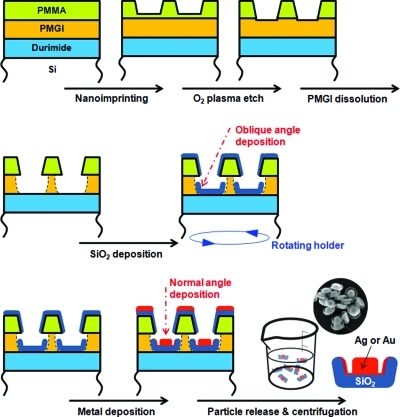
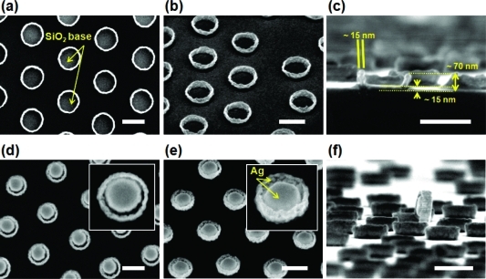
The process for synthesizing these Raman-active nanoparticles is shown in 1 and includes steps for NIL, O2 plasma etching of the residual imprinting resist layer (PMMA), wet chemical development of an undercut resist layer (PMGI), sequential vacuum deposition of SiO2 and Ag, and final release of nanoparticles. In the first step, NIL is used to define the diameter of the nanoparticles by indenting a thermoplastic PMMA layer, with NIL offering distinct benefits of nanoscale resolution, uniform and reliable pattern generation, and high throughput.18−20 Also, by simply adjusting the NIL mold pillar diameters, it is possible to match the nanoparticle diameter to dimensional resonances for excitation wavelengths varying from UV to near-IR.21−24 After stamp release and resist processing, SiO2 was ion-beam-deposited with a measured thickness of 15 nm over the whole SiO2 base. The sample was mounted at an oblique angle with respect to the SiO2 target and was rotated during the deposition. Due to the oblique incidence of the SiO2 flux and surface diffusion of deposited material toward the undercut cavity walls, both the bottom surface and the lower side walls of PMGI wells are found to be covered conformally by the SiO2 layer. 2 shows scanning electron microscopy (SEM) images of SiO2 bases with uniform shapes and sizes that were rigid enough to be successfully generated and observed following removal of PMMA and PMGI resists. Next, a 1 nm thick Ta layer was ion-beam-deposited at normal incidence on the SiO2 base to promote adhesion of a subsequently deposited 50 nm thick Ag film. SEM images in 2 show the fabricated Raman-active nanoparticles after the patterning resists are stripped. Because most of arriving Ag flux, which is all ejected from a Ag target by a 1 keV Xe+ beam, passes through the patterned PMMA layer at near normal incidence, a disk-like Ag core of almost the same diameter as the NIL mold was formed at center of the SiO2 base. The dimensions of each Ag core, 110 nm diameter and 50 nm height, were chosen for efficient extinction of a 532 nm excitation laser.21,22,24,25 In addition to depositing at normal incidence on the exposed substrate area, some Ag atoms scatter off Xe atoms (2 × 10⁻⁴ Torr ambient) in transit and are non-normally incident. In addition, these energetic arriving atoms diffuse laterally on the growing film before equilibrating, so both vapor phase scattering and surface diffusion mechanisms contribute to deposition on the interior side walls of the SiO2 bases, simultaneously with the formation of Ag cores. Deposition methods that avoid metallization of side walls will be described later. The tilted-view SEM image in 2 shows the granular Ag films that cover the inside of these SiO2 side walls. The off-center appearance of the Ag core in the SiO2 base occurs due to a built-in misorientation between our sample holder and Ag target, leading to an average non-normal incidence in our deposition chamber. Although the off-center appearance was not initially intended, it provides a continuous variation of the size of the gap between the Ag core and thin Ag side wall film from ∼0 to 10 nm, as is evident in 2 and its inset, and shows that the minimum gap size can be controlled in the sub-10 nm range by adjusting the Ag deposition angle and including sample rotation during deposition, or in the range well above 10 nm by increasing the PMGI undercut (Supporting Information Figure S1). On the basis of their unique shape, these fabricated nanoparticles are herein referred to as Raman sombreros.
Figure 1.
Schematic illustration of the overall process in this study: nanoimprint lithography, plasma etching of residual PMMA layer, wet chemical dissolution of PMGI layer, oblique angle deposition of SiO2, metal deposition, nanoparticle release, and centrifugation. Inset SEM image shows the fabricated nanoparticles after centrifugation.
Figure 2.
SEM images of (a–c) SiO2 bases and (d–f) Ag/SiO2 SERS nanoparticle arrays from view angles of (a,d) 90°, (b,e) 45°, and (c,f) 3° to the sample surface. SiO2 bases were inspected after deposition of SiO2, removal of PMMA and PMGI, and coated with a 2 nm thick AuPd film to prevent charging during SEM. The Ag/SiO2 SERS nanoparticles were observed after deposition of Ag and removal of PMMA and PMGI. The scale bars are 200 nm.
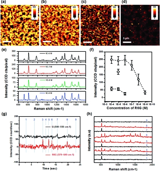
SERS measurements were carried out using Raman sombrero arrays treated with concentrations of R6G ranging from 10–4 to 10–9 M. This treatment involves spreading a 2 μL drop of Raman dye solution over a 9 mm2 area, after which evaporation leaves nonvolatile molecules on the surface (see Methods). We used a scanning confocal microscope coupled to a spectrometer to record Raman spectra at each pixel in the scanned images. Because the nanoparticle pitch is about 400 nm, which is larger than the size of each pixel (250 nm square) and the calculated confocal spot diameter of 240 nm (≈0.4λ/NA, with NA = numerical aperture = 0.9), we can assume that the SERS signal for each pixel was typically generated by a single nanoparticle. SERS maps in 3 show the spatial distribution of the Raman intensity, integrated over frequency shifts between 590 and 640 cm–1, which originates from an in-plane bending of the xanthene ring in the R6G molecule.26,27 The overall appearance of the SERS maps is very similar to the low-magnification SEM images of patchy substrates (Supporting Information Figure S2). The continuously connected nature of the yellow/orange colored regions in these Raman maps corresponds to areas of closely packed nanoparticles in SEM images, while isolated dark spots in Raman maps correspond to non-imprinted regions that appear as isolated bare Si patches in SEM images. These bare patches are commonly observed when NIL molds are made using self-assembled colloidal nanospheres.28,293 shows representative spectra from four different concentrations of R6G coating solutions. Peak positions in these spectra were precisely assigned to the reported vibrational bands of R6G molecules.26,27 Intensities of every peak increased with the concentration of R6G and eventually saturated above 10–6 M, except for the leftmost (520 cm–1) peak from the Si substrate. The intensity change with R6G concentration is summarized in 3. To plot these data, we selected 1000 pixels from each SERS map to exclude bare Si regions and averaged the peak Raman intensity at a shift of 615 cm–1 (Supporting Information Figure S3). The increase and saturation of the Raman signal with dye coverage is consistent with other reports.30,31
Figure 3.
(a–d) Two-dimensional intensity map of SERS signal between 590 and 640 cm–1 from the Ag Raman sombrero nanoparticle array treated with different concentrations of Rhodamine 6G; (a) 10–5 M, (b) 10–7 M, (c) 10–8 M, and (d) 10–9 M. The scale bar in (a–d) is 5 μm. (e) SERS spectra of different concentrations of Rhodamine 6G from bright single pixels, which correspond to single Ag nanoparticles. Baseline signals are corrected. (f) Averaged SERS intensities of the peak of 615 cm–1 from the Raman sombrero nanoparticle (circle), nanodisk (square), and the combined Raman sombrero–SAF magnetic nanoparticle (diamond). (g) Temporal change of Raman intensity from Si (black colored line) and R6G (red colored line) for 25 s. (h) SERS spectra at selected times indicated as dashed lines in (g).
At the concentration of 10–9 M, which corresponds to an average of three molecules per single Raman sombrero nanoparticle for random adsorption of R6G on both Si surface and Ag sombrero nanoparticles (see Supporting Information), the bright contrast from closely packed regions (3) and the characteristic Raman peaks of R6G (3) are still clearly observed. This means that we are able to detect a few R6G molecules for a single Raman sombrero nanoparticle. Consistent with this “few molecule” detection capability, the sample of 3 produced time-dependent on/off blinking behavior where the fluctuating signals were either present or absent, rather than exhibiting a number of variable levels, as is common for “few molecule” systems.7,32−343 shows temporal changes of Raman intensity from R6G over 25 s intervals. As compared to the constant Si signal, the temporal profiles of the R6G intensity show several spikes that originate from Raman scattering by a few molecules. To illustrate this, SERS spectra at selected time points, indicated as dashed lines in 3, are presented in 3. Red colored spectra clearly show a R6G Raman signal. The average time duration of strong scattering is about 220 ms. On the basis of this blinking behavior, we can say that the sombrero nanoparticles provide signals from a single or a few molecules, even though this does not imply that the sombrero nanoparticles can detect every single molecule. For example, if we change our assumption of the random molecular adsorption to the preferred adsorption of R6G on metal surfaces, the number of R6G on a single sombrero could increase up to 20 at the concentration of 10–9 M. Even in that case, the time-dependent on/off signal in 3 means that one or a few molecules among the 20 are sitting on or near a hot spot, and signal enhancement from a hot spot of the sombrero is sufficiently large to detect that blinking signal. Furthermore, we checked SERS maps of the sample treated with more dilute R6G solutions and could detect Raman signals even at 1 pM, which corresponds 1 molecules/10 μm2 (Supporting Information Figure S4). Thus, the blinking behavior in 3 and Raman signals from 1 pM treatment convince us that these signals arise from a few molecules on a single nanoparticle, even though the method used for R6G surface treatment cannot guarantee uniform molecular coverage. The enhancement factor of the Raman sombrero nanoparticle is estimated at about 1.0 × 10⁷ from the relative intensity of fluorescence and SERS (see Supporting Information Figure S5 and related text), in agreement with the stated minimum required enhancement of 106 to 108 for detecting single molecules under molecular resonance conditions.35−37
To isolate the effect of the unique shape of the Raman sombrero nanoparticle, Ag nanodisks were fabricated with the same NIL mold used for the sombrero nanoparticles, but without the sharp sombrero brims. To do so, we used evaporated Ag films without SiO2 bases and found that the resulting nanoparticles have smooth edge profiles, as shown in Supporting Information Figure S6. SERS maps for these Ag nanodisk arrays, also treated with the different concentrations of R6G, were obtained by identical procedures. As indicated by the square data points in 3, the minimum detection level of R6G increased by 3 orders of magnitude, changing from a few molecules per Raman sombrero nanoparticle to a few thousand molecules per nanodisk. Concomitantly, the intensity of Raman signals at dye saturation levels was only about 20% of those for Raman sombreros. The reduced enhancement at saturating dye coverage is not surprising as many adsorbed dye molecules will not have access to hot spots. These results support the notion that the circular perimeter of Raman sombrero nanoparticles functions as a Raman hot spot that increases the overall SERS intensity and enables detection of a few molecules.
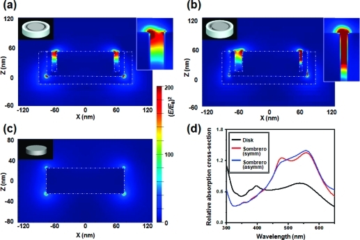
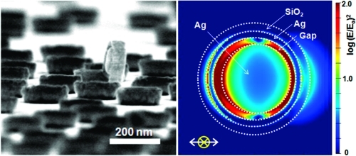
In order to understand the electromagnetic contributions to SERS enhancement, local electric field amplitudes of Ag nanodisks and Raman sombrero nanoparticles in air were modeled using three-dimensional finite-difference time-domain simulations. Nanoparticle shapes and dimensions are based on the SEM images in 2, and details are provided in Supporting Information Figure S7. The direction of incident light is from top to bottom with the electric field polarized in the x-direction. The resulting maps of |E/Eo|2, where Eo and E represent the amplitude of the incident and enhanced electric field, respectively, are shown in 4 for incident light of 530 nm wavelength. The red color between the core and the side wall of the Raman sombrero nanoparticle clearly shows the local electrical field enhancement in the gap. As presented in 4, the off-center appearance of the Ag core offers a further local increase of peak local field enhancement. It is caused by a narrower gap(38) and potentially introduces Fano-type resonances due to the broken symmetry.(39) The simulation results also show that the maximum (E/Eo)4 value of ∼4 × 10⁶ for sombrero nanoparticles is close to the experimentally estimated peak enhancement factor of ∼1 × 10⁷ (Supporting Information Figure S7). The comparison of the maximum value of the (E/Eo)4 value from “a few points” and the measured SERS enhancement from “a few molecules” could be reasonable because the measured SERS signal from a few molecules means one or some of those molecules are placed near a hot spot where the molecule can give a detectable signal. If we consider the SERS signal from “many molecules”, it should be compared with the averaged (E/Eo)4 values, weighted by the area which experiences a given enhancement and not from a few points. In that sense, the averaged (E/Eo)4 value from model calculations, ∼1.1 × 10⁴, from the top surface of the sombrero is well matched with the experimental averaged SERS enhancement factors of 103 to 105 measured for sombreros treated with 10–4 to 10–6 M R6G solution (Supporting Information Figure S7c and related text). We note that this simulation model used bulk dielectric properties of Ag and SiO2 from Palik’s handbook(40) and did not explicitly include a granular morphology for Ag films in order to limit complexity and excessive adjustable parameters. However, the enhancements from granular Ag films(41) or the rough surface of gapped nanostructure(42) are not expected to reach the values observed for the Raman sombreros described here, implying that the sombrero structure provides significant enhancement.
Figure 4.
(a–c) Squared magnitude of the local electrical field amplitude of Ag Raman sombrero nanoparticle (a) with symmetric core, (b) with asymmetric core, and (c) Ag nanodisk. The direction of incident light is from top to bottom and is polarized in the x-direction. (d) Relative absorption cross section of Ag nanodisk (black colored line) and Ag Raman sombrero nanoparticle (red line for symmetric core and blue line for asymmetric core).
4 shows the calculated absorption cross section of Ag nanodisks (black colored line) and Raman sombrero nanoparticles as a function of excitation wavelength (red colored line for symmetric core and blue colored line for asymmetric core). The Raman sombrero nanoparticles are here predicted to absorb more of the incident light at a wavelength of 530 nm than do the nanodisks. It is regrettable that we do not have access to tunable sources to verify the predicted frequency dependence of absorption or Raman scattering directly, which would also help isolate the role of plasmonic effects and Raman dyes, but the important point, from 4, is that a high field is created in the gap between the core and ring and this high field is associated with the efficient excitation of surface plasmons that also gives rise to the increased absorption.
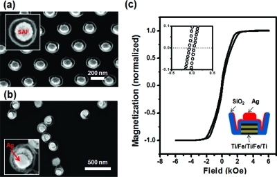
Finally, we demonstrated the addition of a magnetic multifunctionality to this synthetic nanoparticle since chemically synthesized magnetic nanoparticles are widely studied in biology and medicine.43−45 If desirable magnetic properties are combined with the capabilities of our highly sensitive Raman-active nanoparticle, it becomes possible to both manipulate and sense nanoparticles2,4 and possibly even treat cancer cells with external magnetic fields.(46) For incorporating magnetic elements into the Raman sombrero nanoparticle, synthetic antiferromagnetic (SAF) films with the structure of Ti (5 nm)/Fe (10 nm)/Ti (3 nm)/Fe (10 nm)/Ti (5 nm) were evaporated at normal incidence before depositing the SiO2 layer. The antiferromagnetic interaction and orientation of the two ferromagnetic Fe layers within each nanoparticle eliminate remanence, and consequent magnetic aggregation at zero magnetic field, while retaining high saturation magnetic moments.(2)5 shows SAF nanoparticles after coating with a SiO2 overlayer. As familiar from previous results in 2, SiO2 films are conformally deposited on the side wall of PMGI and on the surface of the SAF nanoparticle. The hysteresis loop in 5 is measured by alternating gradient magnetometry at room temperature for substrate-bound nanoparticles and shows the low coercivity, remanence, and the saturation field expected of the composite nanoparticles. Composite SAF/Raman sombrero nanoparticles, which were released from the sample surface, collected, and dried on wafer surfaces, are shown in 5. Because the diameter of the PMMA hole continually decreased during the deposition of SAF and SiO2 layers, the Ag core indicated by the arrow in the inset of 5 is noticeably smaller than the SAF component at the bottom. Although the thickness and size of the Raman component was not optimized, the Raman signals from composite nanoparticles, marked as diamond-shaped data points in 3, are not much different from those of Raman sombrero nanoparticles.
Figure 5.
SEM images of (a) SAF nanoparticles with a SiO2 overlayer, from a 45° tilted view, and (b) combined SAF + Raman sombrero nanoparticles which were released from the sample and solution-deposited onto a Si surface, a top view. Insets in (a) and (b) show the magnified images of each nanoparticle from a top view. (c) Hysteresis loop of substrate-bound nanoparticles measured by alternating gradient magnetometry at room temperature. The inset graph and illustration show a magnified hysteresis loop at near zero field and a schematic cross section of SAF + Raman sombrero nanoparticles, respectively.
Conclusion
In summary, we have presented a highly reliable and cost-effective synthetic approach for fabricating sublithographic feature-enhanced Raman-active nanoparticles. Precisely controlled dimensions and unique internal structure of Ag-based Raman sombrero nanoparticles enable detection of a few R6G molecules. The highly improved sensitivity of our nanoparticle is based on the formation of Raman hot spots at the circular nanogap, which is confirmed by experimental comparison with Ag nanodisk arrays and their simulated electric field amplitudes. Furthermore, because the proposed method uses nanoimprint and vacuum deposition methods which are suitable for mass production, exquisite and affordable control of such nanoparticle structures is expected to become routine. Although the current Raman sombrero nanoparticles were designed for resonance at our 532 nm laser wavelength, the methods proposed in this article can be broadly applied to designs for other wavelengths and dielectric media, and preliminary results for Raman sombreros using Au and a near-IR dye do appear promising. Considering the present results, we expect that Raman sombrero nanoparticles can be used as an ultrasensitive molecular detection platform and that released nanoparticles that contain magnetic elements, distinguishable through the use of different Raman dyes, can be useful as multifunctional in vitro or in vivo imaging reagents.
Methods
Fabrication of Physically Synthesized Raman-Active Nanoparticles
To make a trilayer resist stack, a 50 nm thick preimidized polyimide polymer (Durimide 200, Fujifilm Inc.) was first spin-coated on a Si(100) substrate and baked on a hot plate at 300 °C for 10 min. Next, a 90 nm thick layer of polymethylglutarimide (PMGI, MicroChem) was spin-coated onto the Durimide and baked at 200 °C for 5 min. Finally, a 160 nm thick polymethyl methacrylate (PMMA, Microresist Technology GmbH) resist was spin-coated onto the PMGI and baked at 140 °C for 5 min. For many samples that were not released as synthesized nanoparticles, only the PMMA/PMGI bilayer resist stack on a Si substrate was used. After preparing the resist stack, the coated wafers were subjected to thermal nanoimprinting at 180 °C under a pressure of 40 bar for 60 s, using a commercial nanoimprint tool (NIL2.5, Obducat). A laboratory-made 2 × 2 in.2 Si mold consisting of an array of nanopillars, with 130 nm diameters and 150 nm heights, was used. The details of fabrication methods for Si nanoimprint molds using nanosphere lithography are described in a previous report.(28) After separation of the mold from the wafer surface, the residual PMMA layer was etched by O2 plasma, and the sample was then immersed in a commercial wet chemical developer (LDD-26W, Shipley) for 5 s to form an undercut profile in the PMGI resist and to form flat-bottomed template pores. Next, SiO2 was deposited using 1 keV Xe ion beam deposition at a pressure of 2.5 × 10⁻⁴ Torr. The sample was continuously rotated at an oblique angle, with respect to the SiO2 target, during deposition. Then a 1 nm Ta adhesion layer followed by a 50 nm Ag layer was deposited using 1 keV Xe ion beam deposition. After lift-off in acetone with sonication and removal of PMGI in LDD-26W, the synthesized Raman-active nanoparticle arrays on Si substrates were examined by scanning electron microscopy (SEM, FEI XL30 Sirion). For suspended nanoparticles, the Durimide release layer was dissolved by a commercial solution (S-1165, MicroChem Microposit). The nanoparticles were then collected by multiple cycles of centrifugation (at about 10 000g), solvent exchange, and resuspension in water.
Analysis of SERS Characteristics
A 2 μL droplet of R6G methanol solution was spread uniformly on each 3 × 3 mm2 sample and dried on a hot plate at 90 °C. Due to the low surface tension (∼23 dyn cm–1) and rapid evaporation of methanol, the R6G solution dried quite uniformly over the whole sample surface. Afterward, SERS measurements were carried out using a confocal Raman microscope (alpha500, WITec). R6G-treated sample surfaces were mapped over 25 μm wide square frames, with a unit pixel mesh of 250 nm × 250 nm and an accumulation time of 0.036 s/pixel. To avoid photochemical damage, the power of 532 nm excitation laser was adjusted to 1.4 mW for mapping SERS signals and to 0.6 mW for measuring temporal changes of SERS signals. The power of the excitation laser was measured without objective aperture and lens because of the limited space between objective lens and specimen stage.
Electromagnetic Simulation
Electromagnetic simulations were performed using three-dimensional finite-difference time-domain software (Lumerical FDTD Solution 6.5). The grid was set to a 1.0 nm cubic grid except for critical locations, such as corners and gaps where a 0.5 nm cubic grid was applied. The particles were drawn as shown in Supporting Information Figure S7, which matches the general shape of the experimentally realized particles. The particles in a uniform dielectric medium (n = 1) were illuminated from the top with a linearly polarized plane wave. Scattering and absorption cross sections were calculated and normalized to the particle’s geometric cross section to yield relative cross sections.
Acknowledgments
The authors thank Drs. Christina Zavaleta and Sam Gambhir for their assistance and discussions. This work was supported in part by National Cancer Institute (NCI) Grants 1U54CA119367 and 1U54CA151459 through the Center for Cancer Nanotechnology Excellence at Stanford University, and NCI R33CA138330 grant; by the National Research Foundation of Korea Grant funded by the Korean Government (NRF-2009-352- D00112); and by the World Premier International Center for Materials Nanoarchitectonics (MANA) of the National Institute for Materials Science (NIMS), Tsukuba, Japan. M.Z. thanks financial support from a Stanford Graduate Fellowship.
Supporting Information Available
Additional figures of SEM images, SERS maps, and FDTD calculations. This material is available free of charge via the Internet at http://pubs.acs.org.
Funding Statement
National Institutes of Health, United States
Supplementary Material
References
- Rolland J. P.; Maynor B. W.; Euliss L. E.; Exner A. E.; Denison G. M.; DeSimone J. M. Direct Fabrication and Harvesting of Monodisperse, Shape-Specific Nanobiomaterials. J. Am. Chem. Soc. 2005, 127, 10096–10100. [DOI] [PubMed] [Google Scholar]
- Hu W.; Wilson R. J.; Koh A.; Fu A.; Faranesh A. Z.; Earhart C. M.; Osterfeld S. J.; Han S.-J.; Xu L.; Guccione S.; et al. High-Moment Antiferromagnetic Nanoparticles with Tunable Magnetic Properties. Adv. Mater. 2008, 20, 1479–1483. [Google Scholar]
- Kelly J. Y.; DeSimone J. M. Shape-Specific, Monodisperse Nano-Molding of Protein Particles. J. Am. Chem. Soc. 2008, 130, 5438–5439. [DOI] [PubMed] [Google Scholar]
- Fu. A.; Hu W.; Xu L.; Wilson R. J.; Yu H.; Osterfeld S. J.; Gambhir S. S.; Wang S. X. Protein-Functionalized Synthetic Antiferromagnetic Nanoparticles for Biomolecule Detection and Magnetic Manipulation. Angew. Chem., Int. Ed. 2009, 48, 1620–1624. [DOI] [PMC free article] [PubMed] [Google Scholar]
- Elnathan R.; Kantaev R.; Patolsky F. Synthesis of Hybrid Multicomponent Disklike Nanoparticles. Nano Lett. 2009, 8, 3964–3972. [DOI] [PubMed] [Google Scholar]
- Nie S.; Emory S. R. Probing Single Molecules and Single Nanoparticles by Surface-Enhanced Raman Scattering. Science 1997, 275, 1102–1106. [DOI] [PubMed] [Google Scholar]
- Katrin K.; Wang Y.; Kneipp H.; Perelman L. T.; Itzkan I.; Dasari R. R.; Feld M. S. Single Molecule Detection Using Surface-Enhanced Raman Scattering (SERS). Phys. Rev. Lett. 1997, 78, 1667–1670. [Google Scholar]
- Anker J. N.; Hall W. P.; Lyandres O.; Shah N. C.; Zhao J.; Van Duyne R. P. Biosensing with Plasmonic Nanosensors. Nat. Mater. 2008, 7, 442–453. [DOI] [PubMed] [Google Scholar]
- Qian X.; Peng X.-H.; Ansari D. O.; Yin-Goen Q.; Chen G. Z.; Shin D. M.; Yang L.; Young A. N.; Wang M. D.; Nie S. In Vivo Tumor Targeting and Spectroscopic Detection with Surface-Enhanced Raman Nanoparticle Tags. Nat. Biotechnol. 2008, 26, 83–90. [DOI] [PubMed] [Google Scholar]
- Li J. F.; Huang Y. F.; Ding Y.; Yang Z. L.; Li S. B.; Zhou X. S.; Fan F. R.; Zhang W.; Zhou Z. Y.; Wu D. Y.; et al. Shell-Isolated Nanoparticle-Enhanced Raman Spectroscopy. Nature 2010, 464, 392–395. [DOI] [PubMed] [Google Scholar]
- Fang Y.; Seong N.-H.; Dlott D. D. Measurement of the Distribution of Site Enhancements in Surface-Enhanced Raman Scattering. Science 2008, 321, 388–392. [DOI] [PubMed] [Google Scholar]
- Qin L.; Zou S.; Xue C.; Atkinson A.; Schatz G. C.; Mirkin C. A. Designing, Fabricating, and Imaging Raman Hot Spots. Proc. Natl. Acad. Sci. U.S.A. 2006, 103, 13300–13303. [DOI] [PMC free article] [PubMed] [Google Scholar]
- Wells S. M.; Retterer S. D.; Oran J. M.; Sepaniak M. J. Controllable Nanofabrication of Aggregate-like Nanoparticle Substrates and Evaluation for Surface-Enhanced Raman Spectroscopy. ACS Nano 2009, 3, 3845–3853. [DOI] [PubMed] [Google Scholar]
- Hatab N. A.; Hsueh C.-H.; Gaddis A. L.; Retterer S. T.; Li J.-H.; Eres G.; Zhang Z.; Gu B. Free-Standing Optical Gold Bowtie Nanoantenna with Variable Gap Size for Enhanced Raman Spectroscopy. Nano Lett. 2010, 10, 4952–4955. [DOI] [PubMed] [Google Scholar]
- Su X.; Zhang J.; Sun L.; Koo T. W.; Chan S.; Sundararajan N.; Yamakawa. M.; Berlin A. A. Composite Organic–Inorganic Nanoparticles (COINs) with Chemically Encoded Optical Signatures. Nano Lett. 2005, 5, 49–54. [DOI] [PubMed] [Google Scholar]
- Doering W. E.; Piotti M. E.; Natan M. J.; Freeman R. G. SERS as a Foundation for Nanoscale, Optically Detected Biological Labels. Adv. Mater. 2007, 19, 3100–3108. [Google Scholar]
- Shachaf C. M.; Elchuri S. V.; Koh A. L.; Zhu J.; Nguyen L. N.; Mitchell D. J.; Zhang J.; Swartz K. B.; Sun L.; Chan S.; et al. A Novel Method for Detection of Phosphorylation in Single Cells by Surface Enhanced Raman Scattering (SERS) Using Composite Organic–Inorganic Nanoparticles (COINs). PLoS One 2009, 4, e5206. [DOI] [PMC free article] [PubMed] [Google Scholar]
- Chou S. Y.; Krauss P. R.; Renstrom P. J. Nanoimprint Lithography. J. Vac. Sci. Technol., B 1996, 14, 4129–4133. [Google Scholar]
- Guo L. J. Nanoimprint Lithography: Methods and Material Requirements. Adv. Mater. 2007, 19, 495–513. [Google Scholar]
- Schift H. Nanoimprint Lithography: An Old Story in Modern Times? A Review. J. Vac. Sci. Technol., B 2008, 26, 458–480. [Google Scholar]
- Haynes C. L.; Van Duyne R. P. Nanosphere Lithography: A Versatile Nanofabrication Tool for Studies of Size-Dependent Nanoparticle Optics. J. Phys. Chem. B 2001, 105, 5599–5611. [Google Scholar]
- Lucas B. D.; Kim J.-S.; Chin C.; Guo L. J. Nanoimprint Lithography Based Approach for the Fabrication of Large-Area, Uniformly Oriented Plasmonic Arrays. Adv. Mater. 2008, 20, 1129–1134. [Google Scholar]
- Zheng Y. B.; Juluri B. K.; Mao X.; Walker T. R.; Huang T. J. Systematic Investigation of Localized Surface Plasmon Resonance of Long-Range Ordered Au Nanodisk Arrays. J. Appl. Phys. 2008, 103, 014308. [Google Scholar]
- Schlucker S. SERS Microscopy: Nanoparticle Probes and Biomedical Applications. ChemPhysChem 2009, 10, 1344–1353. [DOI] [PubMed] [Google Scholar]
- Emory S. R.; Haskins W. E.; Nie S. Direct Observation of Size-Dependent Optical Enhancement in Single Metal Nanoparticles. J. Am. Chem. Soc. 1998, 120, 8009–8010. [Google Scholar]
- Hildebrandt P.; Stockburger M. Surface-Enhanced Resonance Raman Spectroscopy of Rhodamine 6G Adsorbed on Colloidal Silver. J. Phys. Chem. 1984, 88, 5935–5944. [Google Scholar]
- Weiss A.; Haran G. Time-Dependent Single-Molecule Raman Scattering as a Probe of Surface Dynamics. J. Phys. Chem. B 2001, 105, 12348–12354. [Google Scholar]
- Earhart C.; Hu W.; Wilson R. J.; Wang S. X.. Self-Assembled Template for High Throughput Nanoimprint Lithography. Digests of the 5th International Conference on Nanoimprint and Nanoprint Technology, San Francisco, 2006; pp 115–116.
- Wang B.; Zhao W.; Chen A.; Chua. S.-J. Formation of Nanoimprinting Mould through Use of Nanosphere Lithography. J. Cryst. Growth 2006, 288, 200–204. [Google Scholar]
- Kneipp K.; Wang Y.; Dasari R.; Feld M. S. Approach to Single Molecule Detection Using Surface-Enhanced Resonance Raman Scattering (SERRS): A Study Using Rhodamine 6G on Colloidal Silver. Appl. Spectrosc. 1995, 49, 780–784. [Google Scholar]
- Lu Y.; Liu G. L.; Kim J.; Mejia Y. X.; Lee L. P. Nanophotonic Crescent Moon Structures with Sharp Edge for Ultrasensitive Biomolecular Detection by Local Electromagnetic Field Enhancement Effect. Nano Lett. 2005, 5, 119–124. [DOI] [PubMed] [Google Scholar]
- Maruyama Y.; Ishikawa M.; Futamata M. Thermal Activation of Blinking in SERS Signal. J. Phys. Chem. B 2004, 108, 673–678. [Google Scholar]
- Emory S. R.; Jensen R. A.; Wenda T.; Han M.; Nie S. Re-examining the Origins of Spectral Blinking in Single-Molecule and Single-Nanoparticle SERS. Faraday Discuss. 2006, 132, 249–259. [DOI] [PubMed] [Google Scholar]
- Lim D.-K.; Jeon K.-S.; Kim H. M.; Nam J.-M.; Suh Y. D. Nanogap-Engineerable Raman-Active Nanodumbbells for Single-Molecule Detection. Nat. Mater. 2009, 9, 60–67. [DOI] [PubMed] [Google Scholar]
- Etchegoin P. G.; Le Ru E. C. A Perspective on Single Molecule SERS: Current Status and Future Challenges. Phys. Chem. Chem. Phys. 2008, 10, 6079–6089. [DOI] [PubMed] [Google Scholar]
- Pieczonka N. P. W.; Aroca R. F. Single Molecule Analysis by Surfaced-Enhanced Raman Scattering. Chem. Soc. Rev. 2008, 37, 946–954. [DOI] [PubMed] [Google Scholar]
- Camden J. P.; Dieringer J. A.; Wang Y; Masiello D. J.; Marks L. D.; Schatz G. C.; Van Duyne R. P. Probing the Structure of Single-Molecule Surface-Enhanced Raman Scattering Hot Spots. J. Am. Chem. Soc. 2008, 130, 12616–12617. [DOI] [PubMed] [Google Scholar]
- Hao F.; Nordlander P.; Burnett M. T.; Maier S. A. Enhanced Tunability and Linewidth Sharpening of Plasmon Resonances in Hybridized Metallic Ring/Disk Nanocavities. Phys. Rev. B 2007, 76, 245417. [Google Scholar]
- Hao F.; Nordlander P.; Sonnefraud Y.; Van Dorpe P.; Maier S. A. Tunability of Subradiant Dipolar and Fano-Type Plasmon Resonances in Metallic Ring/Disk Cavities: Implications for Nanoscale Optical Sensing. ACS Nano 2009, 3, 643–652. [DOI] [PubMed] [Google Scholar]
- Palik E. D.Handbook of Optical Constants of Solids; Academic Press: New York, 1985. [Google Scholar]
- Van Duyne R. P.; Hulteen J. C.; Treichel D. A. Atomic Force Microscopy and Surface-Enhanced Raman Spectroscopy. I. Ag Island Films and Ag Film over Polymer Nanosphere Surfaces Supported on Glass. J. Chem. Phys. 1993, 99, 2101–2115. [Google Scholar]
- Li S.; Pedano M. L.; Chang S.-H.; Mirkin C. A.; Schatz G. C. Gap Structure Effects on Surface-Enhanced Raman Scattering Intensities for Gold Gapped Rods. Nano Lett. 2010, 10, 1722–1727. [DOI] [PubMed] [Google Scholar]
- Lewin M.; Carlesso N.; Tung C. H.; Tang X. W.; Cory D.; Scadden D. T.; Weissleder R. Tat Peptide-Derivatized Magnetic Nanoparticles Allow In Vivo Tracking and Recovery of Progenitor Cells. Nat. Biotechnol. 2000, 18, 410–414. [DOI] [PubMed] [Google Scholar]
- Lee J.-H.; Huh Y. M.; Jun Y. W.; Seo J. W.; Jang J. T.; Song H. T.; Kim S.; Cho E. J.; Yoon H. G.; Suh J. S.; et al. Artificially Engineered Magnetic Nanoparticles for Ultra-sensitive Molecular Imaging. Nat. Med. 2007, 13, 95–99. [DOI] [PubMed] [Google Scholar]
- Gaster R. S.; Hall D. A.; Nielsen C. H.; Osterfeld S. J.; Yu H.; Mach K. E.; Wilson R. J.; Murmann B.; Liao J. C.; Gambhir S. S.; et al. Matrix-Insensitive Protein Assays Push the Limits of Biosensors in Medicine. Nat. Med. 2009, 15, 1327–1332. [DOI] [PMC free article] [PubMed] [Google Scholar]
- Kim D.-H.; Rozhkova E. A.; Ulasov I. V.; Bader S. D.; Rajh T.; Lesniak M. S.; Novosad V. Biofunctionalized Magnetic-Vortex Microdiscs for Targeted Cancer-Cell Destruction. Nat. Mater. 2010, 9, 165–171. [DOI] [PMC free article] [PubMed] [Google Scholar]
Associated Data
This section collects any data citations, data availability statements, or supplementary materials included in this article.


