Abstract
Inductive power transmission is widely used to energize implantable microelectronic devices (IMDs), recharge batteries, and energy harvesters. Power transfer efficiency (PTE) and power delivered to the load (PDL) are two key parameters in wireless links, which affect the energy source specifications, heat dissipation, power transmission range, and interference with other devices. To improve the PTE, a 4-coil inductive link has been recently proposed. Through a comprehensive circuit based analysis that can guide a design and optimization scheme, we have shown that despite achieving high PTE at larger coil separations, the 4-coil inductive links fail to achieve a high PDL. Instead, we have proposed a 3-coil inductive power transfer link with comparable PTE over its 4-coil counterpart at large coupling distances, which can also achieve high PDL. We have also devised an iterative design methodology that provides the optimal coil geometries in a 3-coil inductive power transfer link. Design examples of 2-, 3-, and 4-coil inductive links have been presented, and optimized for 13.56 MHz carrier frequency and 12 cm coupling distance, showing PTEs of 15%, 37%, and 35%, respectively. At this distance, the PDL of the proposed 3-coil inductive link is 1.5 and 59 times higher than its equivalent 2- and 4-coil links, respectively. For short coupling distances, however, 2-coil links remain the optimal choice when a high PDL is required, while 4-coil links are preferred when the driver has large output resistance or small power is needed. These results have been verified through simulations and measurements.
Keywords: Wireless power transmission, implantable microelectronic devices, power transfer efficiency, inductive links
I. Introduction
Inductive power transmission can be used to either continuously power up a device or temporarily recharge its batteries without any direct electrical contact between the energy source and that device. A high efficiency power amplifier (PA), connected to the main energy source on the transmitter side (Tx), often drives the primary coil, which is mutually coupled to a secondary coil on the receiver side (Rx), which is connected to the load (RL). The load can cover a wide range of applications from high performance and sophisticated implantable microelectronic devices (IMD) with relatively high power consumption (>100 mW), such as cochlear and retinal implants, to simple and low power radio frequency identification (RFID) tags that cannot use primary batteries due to their cost, size, or lifetime constraints [1]-[6].
The mutual inductance between a pair of coupled coils, M, is proportional to d−3, where d is the center-to-center spacing between the coils when they are in parallel planes and perfectly aligned [5]. A key requirement in all of the above applications is to deliver sufficient power to the load with high power transfer efficiency (PTE) when d is relatively large or the coils are misaligned, i.e. when M is very small (PTE is already large enough for small d). Large PTE is meant to reduce heat dissipation within the coils, tissue exposure to AC magnetic field, which can cause additional heat dissipation in IMDs, size of the main energy source, and interference with nearby electronics to satisfy regulatory requirements [7]-[9].
Design, theoretical analysis, and geometrical optimization of the conventional 2-coil inductive links have been covered extensively in the literature over the last three decades [10]-[21]. More recently, a 4-coil power transmission link was proposed in [22] to further increase the PTE, particularly at large d. In the 4-coil arrangement, which schematic diagram is shown in Fig. 1a, a pair of coils is used on the Tx side, which are referred to as the driver, L1, and primary, L2, coils. A second pair of coils is used on the Rx side, which are referred to as the secondary, L3, and load, L4, coils. All of these coils are tuned at the same resonance frequency, f0, using capacitors C1 ~ C4. The coils’ parasitic resistances are also shown by R1 ~ R4. The 4-coil method has so far been adopted for transferring power to multiple small receivers, transcutaneous power transmission for d = 10~20 mm, and recharging mobile devices in [23], [24], and [25], respectively. However, an in-depth comparative circuit analysis of this arrangement that can guide a design and optimization scheme for such applications is still lacking.
Fig. 1.
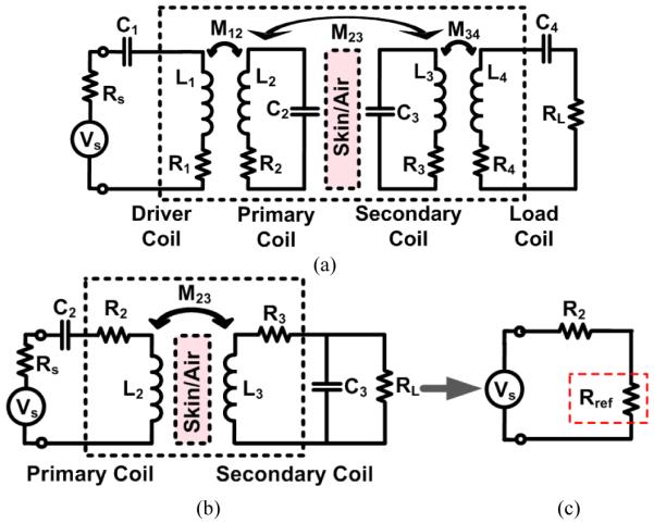
Lumped circuit models of (a) 4-coil and (b) conventional 2-coil inductive links for wireless power transfer. (c) Equivalent circuit of the reflected load on to the primary loop at resonance (for the sake of simplicity, Rs, which is a property of the driving circuitry, has been merged with R2).
In this paper, we have analyzed the 4-coil inductive link utilizing the reflected load theory [5], which is more familiar to circuit designers than the coupled-mode theory used by the physicists in [26], and compared it with its conventional 2-coil counterpart. Our analysis shows that utilizing the 4-coil method increases the PTE at large d at the cost of a significant reduction in the power delivered to the load (PDL). Therefore, unless the application requires a small amount of power (10s of mW or less), a high driving voltage (Vs) will be required, which can reduce the driver efficiency and lead to safety issues in medical applications. Instead, we have demonstrated that a 3-coil inductive power transfer link, initially proposed in [26], not only provides as high PTE as the 4-coil method but also offers a PDL that is significantly higher than both 2- and 4-coil links at large d. In the following section we have constructed a circuit-based theoretical framework to analyze and compare 2-, 3-, and 4-coil inductive links. Section III describes the design and optimization procedure for the 3- and 4-coil inductive links. Measurement results are included in section IV, followed by discussions and concluding remarks in sections V and VI, respectively.
II. Theory of Multiple Inductively Coupled Coils
Fig. 1b shows the simplified schematic diagram of a 2-coil inductive link. It is known that the highest PTE across this link can be achieved when both LC tanks are tuned at the same resonance frequency, [18]. The effect of the Rx side on the Tx side can be modeled at resonance by calculating the reflected impedance,
| (1) |
where , Q2 = ω0L2/R2 , and Q3L = Q3QL/(Q3+QL), in which Q3 = ω0L3/R3 and QL = RL/ω0L3 [5]. QL is often referred to as the load quality factor, and the value for M23 can be calculated from (31) in the Appendix. Hence, the primary loop can be simplified at resonance as the circuit shown in Fig. 1c. It should be noted that R2 in Fig. 1c also includes Rs, the output impedance of the driver circuitry, Vs.
To derive an equation for the PTE at resonance, we should consider that the power provided by Vs divides between R2 and Rref, and the power delivered to Rref, i.e. the power that is received by the secondary loop, divides between R3 and RL, which are the only power consuming components on the Rx side. This will lead to [18]
| (2) |
Note that the first and second terms in (2) correspond to the power division between R2 and Rref, and R3 and RL, respectively.
The amount of power delivered to the load (PDL), on the other hand, can be calculated by multiplying the power provided by Vs, i.e. , by the PTE from (2)
| (3) |
The resonant energy exchange between two conductive objects has been analyzed based on the coupled-mode theory (CMT) in [28]. Utilizing this theory, the PTE between a pair of capacitively loaded conducting loops, such as L2 and L3 spaced by a certain distance, d, can be found from [26], [28]
| (4) |
where Γ = ω0/2Q is the resonance width due to the loop’s intrinsic loss and is the coupling rate between the two loops. It can be shown that (4) will result in (2) if we substitute Γ2 = ω0/2Q2, Γ3 = ω0/2Q3, ΓL = ω0/2QL and K = ω0k23/2 [29].
If the simple 2-coil inductive link in Fig. 1b is extended to an m-coil link, in which 1st and mth coils are connected to the energy source and load, respectively, the reflected load from the (j+1)th coil to the jth coil can be found from
| (5) |
where kj,j+1 is the coupling coefficient between the jth and (j+1)th coils and all coils are tuned at the same resonance frequency, f0. Q(j+1)L is the loaded quality factor of the (j+1)th coil which can be found from
| (6) |
where Qj = ω0Lj/Rj and Rj are the unloaded quality factor and parasitic series resistance of the jth coil, Lj, respectively. It should be noted that for the last coil, which is connected to the load in series, QmL = ω0Lm/(Rm+RL) and for the first coil, which is connected to the source, R1 also includes the source output impedance, Rs. Therefore, assuming that the coupling between non-neighboring coils is negligible, the PTE from the jth coil to (j+1)th coil can be written as
| (7) |
Using (5), (6), and (7), the overall PTE in such a multi-coil inductive link can be found from
| (8) |
and the PDL from
| (9) |
For (8) and (9) to be valid, all coils should be tuned at the same resonance frequency to also achieve the highest PTE and PDL between each neighboring pair of coils [18], and maximize the PTE and PDL of the multi-coil link.
A. Optimal 2-Coil Power Transfer Link
The PTE profile of the 2-coil inductive link according to (2) is a monotonically decreasing function of the coils’ coupling distance, d23. However, for a given set of Q2, Q3 and k23 values, there is an optimal load, RL,PTE = ω0L3QL,PTE, which can maximize the PTE at that particular d23. QL,PTE can be found by calculating the derivative of (2) vs. QL from
| (10) |
The maximum PDL at a certain d23 can be achieved when the reflected impedance from (1) matches the primary coil impedance, i.e. Rref = R2 [30]. It should also be noted that in this condition, the PTE is always less than 50%, because half of the power is dissipated in R2. Thus, the coupling coefficient which maximizes PDL for a certain RL can be found from,
| (11) |
Alternatively, by calculating the derivative of (3) vs. QL, one can find the optimal load, RL,PDL = ω0L3QL,PDL, which can maximize the PDL at a particular d23, where
| (12) |
It is important to note that according to (10) and (12), the maximum PTE and PDL cannot be achieved simultaneously with the same RL or d23. In the 2-coil links, each of these conditions requires a specific set of k23, Q2, and Q3, which may not be feasible within the designated constraints. On the other hand, a multi-coil solution provides the designer with more degrees of freedom to optimize the inductive link based on either one of the above requirements. This is the basic idea behind the 3- and 4-coil inductive links, despite their potential negative impact on the size-constrained applications.
B. 4-Coil Power Transfer Inductive Link
The PTE in the 4-coil inductive link, shown in Fig. 1a, can be found by reflecting the resistive components to the left from the load coil back to the driver coil loop, one stage at a time using (5), and calculating the portion of the power that is delivered to the following stage, using (7), until it reaches RL
| (13) |
To simplify this equation, k13, k14 and k24 have been neglected in comparison to coupling coefficients between neighboring coils, which are k12, k23 and k34 [24]. Using the same method, the PDL in the 4-coil inductive link can be found from
| 14) |
The PTE between loosely coupled primary and secondary coils, L2 and L3, is the dominant factor in determining the overall PTE of the 4-coil link at a large coupling distance, d23. When RL reflects onto L3 from L4 according to (5), it reduces the quality factor of L3 from Q3 = ω0L3/R3 to
| (15) |
based on (6). In order to maximize the PTE between L2 and L3, Q3L in (15) should satisfy (10). k34 in (15) is, therefore, a key parameter in 4-coil links which allows designers to maximize the PTE for any arbitrary RL. As mentioned in section II.A, this flexibility is not available in a 2-coil link. Similarly, the total impedance in the secondary coil reflects onto the primary coil, based on (5), and reduces the primary coil’s quality factor from Q2 = ω0L2/R2 to
| (16) |
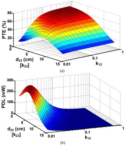
From (16) and (7) it can be inferred that a strong coupling between the primary and secondary coils (i.e. a high k23) reduces Q2L and consequently η12, which is the PTE between L1 and L2. It should also be noted that according to (16), Q2L is roughly proportional to , where k23 is further proportional to [5]. Therefore, Q2L is proportional to , implying that η12 will significantly reduce at small d23 if k12 is not chosen large enough. This effect has been demonstrated in Fig. 2a, which shows the PTE of a 4-coil inductive link as a function of k12 and d23 for the coils used in our measurements and specified in Table I. It can be seen that for small k12, near the origin, the PTE has dropped at short coupling distances due to the small η12. Therefore, small Q1 and k12 will result in a significant drop in η12 at small coupling distances according to (7).
Fig. 2.
Simulated (a) power transfer efficiency (PTE) and (b) power delivered to the load (PDL) for a 4-coil inductive link as a function of k12 and d23 when k34 = 0.22 for the coils specified in Table I. Vs = 1 V and RL = 100 Ω.
Table I.
Optimized Geometries for Design Examples
| Parameters | Symbols | 2-Coil | 3-Coil / 4-Coil | |||
|---|---|---|---|---|---|---|
| Meas | Optim | Meas | Optim | |||
| L1 | Inductance (μH) | Lj | - | - | - / 0.9 | - / 0.18 |
| Outer diameter (cm) | D01 | - | - | - / 16.8 | - / 10.5 | |
| Fill factor | φ 1 | - | - | - / 0.13 | - / 0.14 | |
| Num. of turns | n1 | - | - | - / 2 | - / 1 | |
| Line width (mm) | W1 | - | - | - / 8.66 | - / 12 | |
| Line spacing (mm) | S1 | - | - | - / 2.6 | - / 35 | |
| Quality factor | Q1 | - | - | - / 255 | - / 131 | |
| L2 | Inductance (μH) | L2 | 0.9 | 1.2 | 0.9 | 1.2 |
| Outer diameter (cm) | D02 | 16.8 | 27 | 16.8 | 27 | |
| Fill factor | φ 2 | 0.13 | 0.28 | 0.13 | 0.28 | |
| Num. of turns | n2 | 2 | 2 | 2 | 2 | |
| Line width (mm) | W2 | 8.66 | 12 | 8.66 | 12 | |
| Line spacing (mm) | S2 | 2.6 | 35 | 2.6 | 35 | |
| Quality factor | Q2 | 255 | 196 | 255 | 196 | |
| L3 | Inductance (μH) | L3 | 0.12 | 0.058 | 0.4 | 0.47 |
| Coil diameter (cm) | D03 | 4 | ||||
| Wire diameter (mm) | w3 | 0.64 | 5.68 | 0.64 | 2.2 | |
| Num. of turns | n3 | 1 | 1 | 2 | 3 | |
| Line spacing (μm) | S3 | 100 | 100 | 100 | 100 | |
| Quality factor | Q3 | 105.2 | 151.5 | 111 | 417 | |
| L4 | Inductance (μH) | L4 | - | - | 0.4 | 0.22 |
| Coil diameter (cm) | D04 | - | - | 4 | 2.8 | |
| Wire diameter (mm) | W4 | - | - | 0.64 | 1 | |
| Num. of turns | n4 | - | - | 2 | 2 | |
| Line spacing (μm) | s4 | - | - | 100 | 100 | |
| Quality factor | Q4 | - | - | 177 | 142 | |
| L1 - L2 coupling distance (mm) | d12 | - | - / 1.5 | |||
| L2 - L3 coupling distance (mm) | d23 | 120 | ||||
| L3 - L4 coupling distance (mm) | d34 | - | 9 | |||
| Power transfer efficiency (%) | η | 15 | 27.4 | 37/35 | 55/54 | |
| Power delivered to load (mW) | PDL | 170 | 160 | 260/4.4 | 146/6.8 | |
| Nominal load (Ω) | RL | 100 | ||||
| Driver output resistance (Ω) | RS | 0.1 | ||||
| Power carrier frequency (MHz) | fo | 13.56 | ||||
L1 and L2 are hexagonal overlapping PSCs, while L3 and L4 are WWCs.
Grayed cells indicate the design constraints.
In order to avoid the above problem, k12 should be kept large, which according to (5) results in a large reflected load onto L1. This can reduce the available power from the source, according to (9), unless Vs is increased. However, large Vs can cause safety issues in medical applications, and this is a major disadvantage of the 4-coil arrangement for inductive power transfer to IMDs, particularly when a high PDL is required.
Fig. 2b shows the PDL from (14) as a function of k12 and d23 for the coils in Table I. It can be seen that increasing k12 results in reducing the PDL when Vs is kept constant. A comparison between Figs. 2a and 2b is instructive by observing that the high PTE and high PDL areas of these surfaces do not overlap, which means that in a 4-coil inductive link there is always a compromise between the highest PTE that can be achieved while delivering sufficient power to the load without surpassing safe Vs limits. This can be seen in [25] where k12 has been purposely reduced to achieve a high PDL. The result of k12 reduction, however, is a drop in PTE from 70% to 10% in short coupling distances. Thus, considering the above issues and the size overhead, the utility of the 4-coil links in high power IMD applications is questionable.
The optimal PTE with respect to d23 in a 4-coil link can be found by differentiating (13) in terms of k23, which gives
| (17) |
This equation helps designers to shift the peak of the PTE profile in Fig. 2a towards the nominal coupling distance for certain k12 and k34 values. Similarly, the optimal PDL, can be found by differentiating (14) in terms of k23, which results in
| (18) |
C. 3-Coil Power Transfer Inductive Link
The 3-coil inductive link circuit model, which comprises of the primary coil, L2, on the Tx side and the secondary and load coils (L3 and L4) on the Rx side, has been shown in Fig. 3. The PTE of this link with no simplification can be found from
| (19) |
where A, B, and θ are
| (20) |
Also the PDL of the 3-coil inductive link can be found from
| (21) |
If we ignore k24 due to large separation between L2 and L4, then (19) can be simplified to
| (22) |
where
| (23) |
Similarly, (21) can be simplified to
| (24) |
Fig. 3.
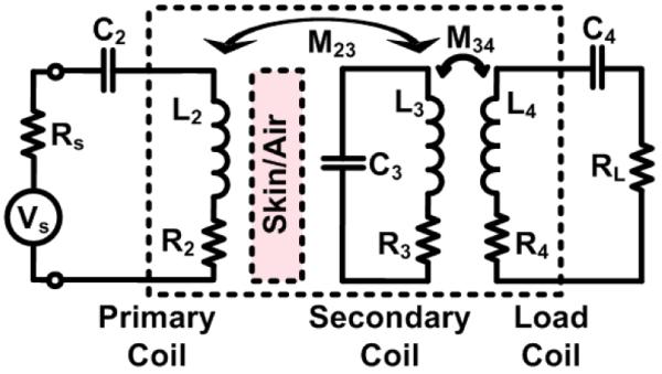
Lumped circuit model of the 3-coil inductive link.
The problem with the optimal 2-coil power transfer link in section II.A was that for a given set of Q2, Q3, and k23, the optimal PTE could only be achieved for a certain load, RL,PTE, which could be far from the nominal RL. In the 3-coil power transfer inductive link, however, L3, L4 and M34 in Fig. 3 can play the role of an impedance matching circuit (compare with Fig. 1b), which can convert any arbitrary RL to RL,PTE. This is equivalent to having a load quality factor of QL = QL,PTE in the secondary loop of a 2-coil link, which was defined in (10).
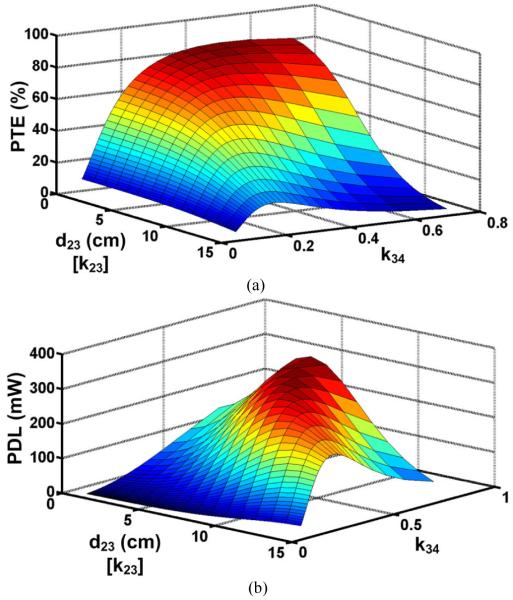
This leverage in the design of the 3-coil links has been provided by term in (22)-(24). Lowering tends to increase η23 and at the same time reduces η34 in (23), both of which affect the overall PTE in (22). To better understand the PTE variations in a 3-coil inductive link, the effects of k34 and d23 on the PTE are shown in Fig. 4a for the coils specified in Table-I. The optimal value for that maximizes the PTE for a certain d23 (or k23) can be found by differentiating (22) with respect to k34,
| (25) |
For a certain RL, if the choice of k34 in the design of a 3-coil inductive link satisfies (25), then the reflected load onto the secondary loop will satisfy (10) and maximizes the PTE.
Fig. 4.
Simulated (a) PTE and (b) PDL for a 3-coil inductive link as a function of k34 and d23 for the coils in Table I. Vs = 1 V and RL = 100 Ω.
Fig. 4b shows the effects of k34 and d23 on the PDL of the 3-coil inductive link in Table-I, based on (24). It can be seen that there are optimal values for both k34 and k23, which can maximize PDL, and in order to find them, (24) should be differentiated with respect to k34 and k23,
| (26) |
| (27) |
These values result in the reflected load on to the primary coil to be equal to R2, in order to satisfy (12) for any arbitrary RL.
A comparison between Figs. 4 and 2 reveals a key advantage of the 3-coil links over their 4-coil counterparts, which suffer from poor PDL in areas of the curve that PTE is high (see section II.B). Comparing Figs. 4a and 4b, however, shows that by proper choice of k23 and k34, which depend on the coil values and their geometries, designers can establish 3-coil inductive power transfer links that offer both high PTE as well as high PDL. Another advantage of the 3-coil links is that they are not affected by the inefficiency between the driver and primary coils (η12 < 1).
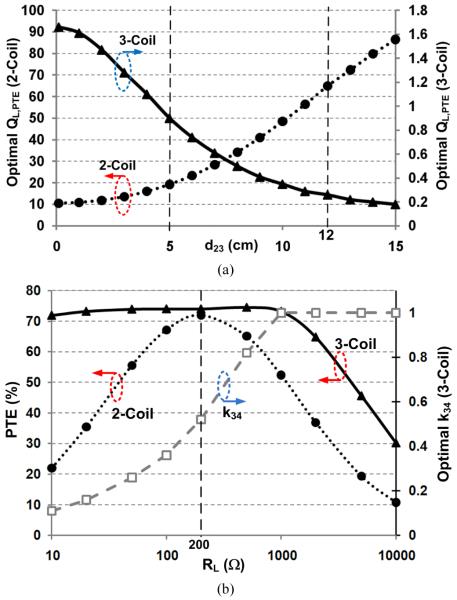
Fig. 5a compares the 2-coil and 3-coil links’ optimal load quality factors, QL,PTE, vs. d23 to maximize the PTE for the coils in Table I. Three important points to learn from these curves are: 1) The 2-coil link needs an exceedingly higher QL,PTE as d23 increases, which may not be feasible, particularly in small coils. On the other hand, the 3-coil link satisfies the PTE optimization requirement at various distances with much smaller QL,PTE, which is quite feasible by connecting RL in series with L4 as shown in Fig. 3. 2) The optimal QL,PTE in the 3-coil link is adjustable with k34 based on (25), as shown in Fig. 5b, where the optimal PTE has been maintained for the 3-coil link in a wide range of RL (10 Ω − 1 kΩ) at d23 = 5 cm. On the other hand, with a 2-coil link the optimal PTE has been achieved in these conditions only for a specific RL,PTE = 200 Ω that satisfies (10). 3) At small d23, the 2-coil link requires smaller QL,PTE, which is relatively easy to achieve. Therefore, for short distance inductive power transmission, which is the case in most transcutaneous IMD applications, a conventional 2-coil inductive link that is properly designed can be very close to the optimal choice [20], [21].
Fig. 5.
(a) Optimal load quality factor, QL,PTE, needed to achieve the highest PTE vs. coils’ spacing in 2- and 3-coil inductive links (k34 = 0.22, RL = 100 Ω, and other parameters from Table I). (b) k34 adjustments based on (25) to maintain the optimal PTE in a 3-coil link vs. RL at d23 = 5 cm. The 2-coil link only reaches the optimal PTE for a specific RL = 200 Ω that satisfies (10).
The additional degree of freedom provided by 3- and 4-coil inductive links via k34 allows designers to increase the loaded quality factor of L3 (Q3L). This leads to better immunity to misalignment but at the same time higher sensitivity to carrier frequency variations or detuning in multi-coil links. Note that misalignment only happens between L2 and L3, because L1 and L2 in 4-coil links and L3 and L4 in 3- and 4-coil links are often housed together in the Tx and Rx sides, respectively. There is also little concern about detuning of L4 and L1 because these coils have very small loaded quality factors and therefore are much less sensitive to frequency shifts.
III. Optimal Design of Multi-Coil Inductive Links
In this section, we extend the design and optimization procedure, which we introduced in [20] for maximizing the PTE in 2-coil wireless power transmission links to multiple coils. Either (19) or (22) can be used for the optimization of PTE in 3-coil links. However, the former can complicate the procedure, which may not be necessary if k24 is very small. As mentioned in [20], most of the design constraints are set by the inductive link application, and the rest of them by the coil fabrication process. For instance, in IMD applications the size of L3 depends on the IMD location in the body. Because to maximize the PTE, the outer diameter of L3, Do3, should be increased to the largest size allowed by the application.
We have provided further details about coils designed for the IMD applications in section V. However, in this section we have chosen an inductively powered wireless neural recording system for freely behaving small animal subjects as our design and optimization example [31]. A key limitation of the current wireless neural recording systems that are developed for neuroscience applications is the need for the animal subject to carry a large payload of batteries for continuous recording over several hours or even days [32] - [34]. This may not be a major issue for larger animal subjects such as non-human primates [35], [36]. However, such a payload can affect the behavior of smaller animals such as rats and mice, which are more common in behavioral neuroscience labs due to their lower cost [37]. The goal here is to substitute the batteries by L3 and L4 in the animal headstage, and L2 at the bottom of the cage. For such an application, we chose Do3, d23, and d34 equal to 4 cm, 12 cm, and 0.9 cm, respectively, as the starting point of this design example (see Table I).
A. Design Procedure
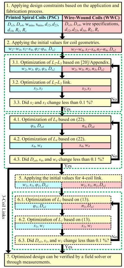
We showed in section II.C that the optimal 3-coil link can be considered as the loosely coupled L2-L3 link when the arbitrary RL is transformed to RL,PTE, utilizing L4 and k34 to satisfy (10). Therefore, the optimization procedure, shown in Fig. 6 flowchart, has two parts: First, η23 is maximized in (23) by maximizing , which requires optimizing L2 and L3 geometries like what we did for a 2-coil inductive link in [20]. Second, the geometry of L4 is optimized for k34 to satisfy (25), and consequently maximize η34 in (23) by maximizing .
Fig. 6.
Iterative multi-coil inductive link design optimization flowchart.
One of the decisions that should be made early on is whether the coils are lithographically defined or wire-wound. Geometrical parameters of the printed spiral coils (PSC) that affect circuit parameters such as Q and k, and consequently the PTE, are the line width (w), line spacing (s), outer diameter (Do), and fill factor (φ: the ratio between the difference and the sum of a PSC’s inner and outer diameters), which are described in [20]. In wire-wound coils (WWC) made of single filament solid wires, w is the wire diameter, the number of turns (n: integer) is used instead of φ, and s can be twice the thickness of the wire insulation. The relationship between circuit parameters and the coil geometries in this case can be found in the Appendix. In each step of this optimization scheme, the designer should derive k, Q, and other circuit parameters from the PSC and WWC geometries using the equations presented in [20] and the Appendix, respectively. Moreover, to consider the finite quality factor of the resonance capacitors (C1-4) and the resistance of their connections to the coils, an additional 0.1 Ω was added to R1-4 values.
In step-1, design constraints imposed by the application and coil fabrication technology are considered. The former defines the maximum values for Do3 and Do4, while the latter indicates the minimum line width and line spacing (wmin, smin) in the case of PSC, or the wire specifications in WWC. The nominal values for d12, d23, d34, RL and Rs are also required in this step, which are dependent on the application (d12 is needed only for 4-coil links). For instance, d34 will depend on the implant thickness in IMD applications if L3 and L4 are going to be housed together. As mentioned earlier, Rs, which is a property of the driving circuitry, should be added to R2 and R1 in our procedure for the design of 3- and 4-coil links, respectively.
In step-2, the initial values for L2~L4 geometries are chosen, which are (w2~w4, s2~s4, φ2~φ4, Do2) and (w2~w4, s2~s4, n2~n4, Do2) for PSCs and WWCs, respectively. A more detailed discussion about how to choose these initial values can be found in [20].
L2 and L3 geometries are optimized in step-3 for η23,max. In step-3.1, following the procedure in [20] provides the optimal values of (w2, w3, φ2, φ3, Do2) for PSCs. Running the same iterative procedure while replacing (φ2, φ3) with (n2, n3) in the Appendix provides the optimal values of (w2, w3, n2, n3, Do2) for WWCs. In step-3.2, values found in step-3.1 are used to sweep s2 and s3 in [20] or in the Appendix for PSCs or WWCs, respectively, such that the resulting k23, Q2, and Q3 maximize . The new s2 and s3values are then fed back into step 3.1 to improve η23 further. Steps 3.1 and 3.2 are repeated iteratively until s2 and s3 values change less than 0.1% and satisfy the condition in step-3.3.
In step-4, the geometry of L4 is optimized using L2 and L3 circuit parameters from step-3, such that the resulting k34, R4, and Q4 satisfy (25). In step-4.1 for PSCs, φ4 and Do4 are swept in [20] for the resulting k34 and Q4 to maximize η3-coil in (22). Similarly for WWCs, n4 and Do4 are swept for the resulting k34 and Q4 from the Appendix to maximize η3-coil. In step-4.2, the new φ4 and Do4 values found in step-4.1 for PSCs are used to sweep s4 and w4 in [20] for the resulting k34 and Q4 to further maximize η3-coil in (22). For WWCs, n4 and Do4 values from step-4.1 are used to sweep s4 and w4 in the Appendix for the resulting k34 and Q4 to further maximize η3-coil. Steps 4.1 and 4.2 are repeated iteratively until s4, w4 and Do4 values change less than 0.1% and satisfy the condition in step-4.3. This step concludes the design of the 3-coil wireless power transmission link for maximum PTE, which can be further validated using field solvers, such as HFSS (Ansoft, Pittsburgh, PA).
The rest of steps in Fig. 6 are specific to 4-coil links to optimize the geometry of L1 for the highest PTE based on (13). In step-5, the initial values for L1 geometry, which are (w1, s1, φ1, Do1) and (w1, s1, n1, Do1) for the PSCs and WWCs, respectively, are chosen. Step-6 is quite similar to step-4, which determined the optimal geometry of L4. The iterative process in steps 6.1 and 6.2, and the condition in step-6.3 will ensure η12,max and consequently maximize η4-coil in (13), which can be validated by field solvers.
B. Design Example
Table I summarizes the results of optimization procedure for two sets of 2-, 3- and 4-coil inductive links that operate at f0 = 13.56 MHz and deliver power to a load of RL = 100 Ω as efficiently as possible from a nominal coupling distance of d23 = 12 cm. To discriminate between the losses that are specific to the inductive link and those that are related to the driver circuit, thus out of the scope of this work, we considered a small Rs of only 0.1 Ω in our optimizations to account for the driver output resistance. The effect of Rs on the PTE and PDL of the 2-, 3- and 4-coil inductive links, however, has been discussed in more details in section V. Based on the requirements of our application, the coils on the Tx side were considered overlapping hexagonal shaped PSCs, fabricated on cost effective 1.5 mm thick FR4 printed circuit boards (PCB) with 1-oz copper weight (35.6 μm thick), and those on the Rx side were considered WWCs made of magnet wire (enameled copper).
In these designs, the PCB fabrication process requires wmin and smin to be 150 μm. Also in the case of the 4-coil design, the overlapping L1 and L2 determine d12 by the PCB thickness (see Fig. 9). As mentioned earlier, to limit the size of the headstage, Do3 and d34 were also limited 4 cm and 0.9 cm, respectively. The first set of coils, designated by “optimal” in Table I, are resulted from the iterative optimization process, as shown in Fig. 6, with no additional constraints. According to the equations in section II, the optimized 3- and 4-coil inductive links can achieve PTE of 55% and 54%, respectively, compared to the 2-coil inductive link, which PTE is limited to 27.4% at d23 = 12 cm. Despite their similarity in PTE, a key difference between the 3- and 4-coil links is that the former has a PDL of 146 mW for Vs = 1 V, while the latter can only deliver 6.8 mW to the load because of the large reflected impedance, Rref, onto the driver coil, L1. The PDL of the 2-coil link in these conditions is 160 mW.
Fig. 9.
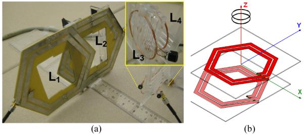
(a) Experimental setup for measuring the PTE and PDL in a 4-coil inductive link. (b) 4-coil inductive link model in the HFSS. Coil specifications are listed in Table I.
In the second set of coils, designated by “measurement”, the PSC diameter on the Tx side (Do1, Do2) was limited to 16.8 cm due to PCB fabrication constraints. The total weight of the Rx coils that are going to be mounted on the animal headstage was limited to W3,4 = 1.6 g, which relate to the WWC geometries according to (39) in the Appendix. Hence, WWC wire diameter on the Rx side (w3, w4) was limited to 0.64 mm (AWG-22) to observe the headstage weight limitation. This set of coils was fabricated and used in section IV measurements.
IV. Simulation and Measurement Results
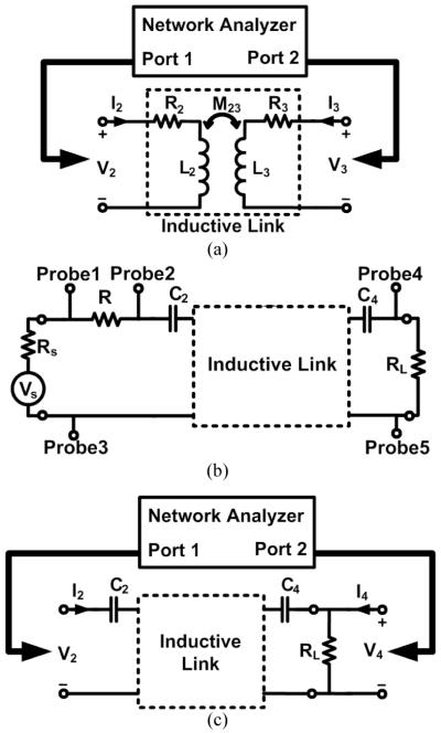
Two types of setups have been used in the past for PTE measurements. In the first method, shown in Fig. 7a, a network analyzer is directly connected to the primary and secondary coils to measure the S-parameters. Then the S-parameters are converted to Z-parameters [38] to obtain,
| (28) |
and find the PTE by substituting them in (2). This method is straightforward, but it does not involve any actual power transfer between the coils. It is bound to the assumptions and accuracy of the models within the theoretical PTE and PDL equations. It also becomes more complicated and less accurate in multi-coil links, which should be tuned at a certain resonance frequency in order to operate properly (see Fig. 1a).
Fig. 7.
PTE measurement setups for inductive links: (a) Conventional method using a network analyzer, (b) direct method using a signal source and current and voltage probe via oscilloscope, (c) the new method using network analyzer with all the coils tuned at the carrier frequency and RL connected.
In the second method, shown in Fig. 7b, a signal generator or PA drives the primary coil, tuned at f0, and the transmitted power is calculated by directly measuring the current and voltage waveforms. The received power can also be found in the same way by probing the voltage across RL. Even though this method is more realistic than the first one, it rapidly loses its accuracy at higher carrier frequencies, such as 13.56 MHz, due to the parasitic components introduced by measurement probes. Moreover, the oscilloscope ground connections can introduce additional complications due to ground loops and interference. Our experiments showed that using different values of R in Fig. 7b for sensing the inductive link input current could result in different values for the PTE and PDL.
We have devised a new method for PTE and PDL measurements, which seems to be more accurate particularly in multi-coil inductive links. In this method, resonance capacitors and RL are connected to the primary and load coils, which are then considered a complete 2-port system along with the multi-coil inductive link, as shown in Fig. 7c. The network analyzer is then used to measure the S-parameters, and consequently the Z-parameters are derived, as in the first method [38]. PTE and PDL are found from 2-port equations,
| (29) |
where Z22 = V2/I2 and Z42 = V4/I2 are derived when I4 = 0. The I4 = 0 requirement in calculating Z-parameters ensures that the network analyzer loading (often 50 Ω) on the inductive link does not affect the results. In this method, as the network analyzer sweeps a certain frequency range that includes f0, actual power transfer does take place in the form of a small signal injected from Port-1 of the network analyzer to RL. One can also measure the entire link power transfer efficiency all the way from the battery to the load by adding the equivalent of the source output resistance, Rs, in series with L1 in the 4-coil link and L2 in the 2- and 3-coil links.
Figs. 8a and 9a show the experimental setup for measuring the PTE and PDL of the 3- and 4-coil inductive links, respectively. These coils were fabricated based on the values listed in the “Measurement” columns of Table I, and held in parallel and perfectly aligned using non-conducting Plexiglas sheets and plastic screws to prevent power loss due to eddy currents. Figs. 8b and 9b show 3-D models of the same coils constructed in the HFSS electromagnetic field simulator for 3- and 4-coil links, respectively. In the 4-coil setup, k12 was adjusted for a fixed d12 = 1.5 mm, by changing the amount of overlapping between similar L1 and L2 (see Fig. 9). L3 and L4 were also similar and provided k34 = 0.22 at d34 = 9 mm.
Fig. 8.
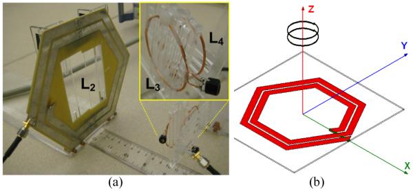
(a) Experimental setup for measuring the PTE and PDL in a 3-coil inductive link. (b) 3-coil inductive link model in the HFSS. Coil specifications are listed in Table I.
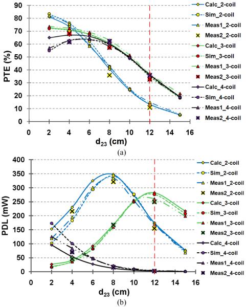
Figs. 10a and 10b compare the measured, simulated (via HFSS), and calculated (see section II) values of the PTE and PDL, respectively, vs. coupling distance, d23, in 2-, 3- and 4-coil inductive links. The curves labeled as “Meas1” show the measurement results according to the method proposed in Fig. 7c, using a ZVB4 network analyzer (R&S, Germany). It can be seen that these results are in very good agreement with HFSS simulation and calculation results, labeled “Sim” and “Calc”, respectively.
Fig. 10.
Comparison between measured, simulated (HFSS), and calculated (see section II) values of the (a) PTE and (b) PDL vs. d23 for 2-, 3-, and 4-coil inductive links specified in the “Measurement” columns of Table I (Vs = 1 V).
As an alternative, we also measured the PTE and PDL of the inductive links according to the method shown in Fig. 7b, using a class-D PA with known power efficiency (ηPA = 30%) and R = 15 Ω for 2- and 3-coil links, and R = 500 Ω for 4-coil link (due to low current levels) in three different distances of 4, 8, and 12 cm, which are labeled as “Meas2” in Fig 10. In this case the measurement results are probably less accurate because of the parasitic components added by the probes and the fact that the PA’s power efficiency has some dependency on the reflected impedance onto the Tx side, which changes with d23. Nonetheless they are close to the other values.
It can be seen in Fig. 10a that the 3- and 4-coil inductive link PTEs (37% and 35%, respectively) are significantly higher than the PTE of the 2-coil link (15%) at d23 = 12 cm. At the same coupling distance, however, the 3-coil inductive link has achieved a PDL of 260 mW from Vs = 1 V, which is 1.5 and 59 times higher than the PDL of 2- and 4-coil links, respectively. Despite its high PTE, the 4-coil link has only been able to deliver 4.4 mW to the load under these conditions, which may not be sufficient for most applications. It thus requires a much higher Vs (~7.7 times in this case) to become comparable to its 3-coil counterpart. It can also be seen from the 2-coil PTE profile in Fig. 10a that short and large distances have smaller PTE variation. However, there is a certain coupling distance in between where the PTE drops very rapidly. The second derivative of (2) can correlate to this distance. Q2 and Q3L should preferably be maximized to move this point to larger distances.
In the 2-coil link used in our measurements, RL = 100 ohm, is connected in parallel with L3 to achieve a higher QL = 9.8. Q3L is only 8.9 and Rref, according to (1), is 0.053 Ω at k23 = 8.8×10⁻³. Thus, (2) estimates η2-coil to be 13.5%. According to Fig. 5a, the optimal QL in this case is 65, which is much larger than the realistic 9.8 value, which can be achieved following our optimization process and applying design constraints.
On the other hand, if we consider the 3-coil inductive link and RL in series with L4, QL = 0.34 which is close to the optimal value for PTE (QL = 0.26) according to Fig. 5a. Rref,34 is 0.56 ohm at k34 = 0.22, which results in η34 = 74.6% based on (5) and (7), respectively. Therefore, Q3 = 177 is loaded to become Q3L = 45.4, based on (6), and remains much higher than Q3L = 8.9 of the 2-coil link. Finally, Rref,23 is 0.28 Ω at k23 = 9×10⁻³, which results in η23 = 48.3% based on (5) and (7). Finally, η3-coil = 0.746×0.483×0.998 = 36%, where 99.8% represents the division of power between R4 and RL. In these conditions, Q2 = 255 reduces to Q2L = 132 based on (6).
In the case of the 4-coil link, Rref,12 and η12 are 41.5 Ω and 99.3% at k12 = 0.064 based on (5) and (7), respectively, which lead to more or less the same PTE as the 3-coil link. Nonetheless, comparing the reflected loads seen by the PA in 2-, 3- and 4-coil links (0.053, 0.28, and 41.5 Ω, respectively) clearly explains the reason for low PDL in the 4-coil link.
If one is interested in calculating the overall efficiency all the way from Vs to RL, including the driver, then Rs = 0.1 Ω should be added to R2, R2, and R1 in (2), (19), and (13) for 2-, 3- and 4-coil links, respectively, which yield PTEs of 11%, 31%, and 35%. These correspond to the PDLs of 98 mW, 187 mW, and 4.4 mW for Vs= 1 V, respectively.
V. Discussion
In Fig. 10a, the 4-coil simulated and measured PTE at small d23 are up to 10% lower than the calculated results. This could be because of approximating the overlapping hexagonal-shaped coils in Fig. 9a with a pair of circular coils (due to their complex geometry) for calculating k12. We found that for these coils, calculations give a higher k12 = 0.09 compared to HFSS simulations, k12 = 0.064. This resulted in larger error at small d23, where the reflected load onto L2 is larger, and a higher k12 can overestimate η12. It is worth noting that the higher estimation of k12 also results in lower available power from the source, leading to the calculated PDL at short coupling distances to be smaller than the simulation and measurement results, as it can be seen in Fig. 10b. Another reason for the discrepancy could be a larger percentage of error in the actual coil distances and alignments at lower d23.
We added the source output resistance, Rs, representing the driver loss, to R1 and R2 in 4- and 2/3-coil links, respectively, to consider its effects on the optimization procedure. The Rs value, which depends on the PA design, plays an important role in optimization of the overall power efficiency, ηov, from the energy source to the load [20]. Other key parameters that affect the PA design are the power required by the load (PL), source voltage (Vs), supply voltage (VDD), transistors breakdown voltage, and safety limits for the IMD applications [16]. The available power from source, Pav, can be expressed as , which implies that large Vs or small Rs are desired when PL is large. In a class-E PA, zero-voltage-switching allows for high power efficiency with peak voltages across the coil and PA transistor that are 1.07 and 3.56 times VDD, respectively [40]. Therefore, when the application involves large PL in the order of 100s of mW, Rs should be reduced to levels well below 1 Ω for the PA to provide sufficient Pav at reasonable Vs and VDD [16], [25].
To compare the effects of Rs on 2-, 3- and 4-coil inductive links optimization, including the PA losses, we have optimized our design example in Table I for different values of Rs from 0.1 to 5 Ω. It can be seen in Fig. 11 that the 4-coil link maintains its high PTE even at large Rs values due to its large reflected impedance, Rref >> Rs, at the cost of very small PDL. On the other hand, for Rs values below 1 Ω, the 3-coil link offers almost the same PTE, while providing much higher PDL. Therefore, we can conclude that for the applications that require small amounts of PDL in the order of 10s of mW, a 4-coil inductive link with a weak driver provides the highest ηov while keeping Vs within reasonable range. Because utilizing large transistors in this case to reduce Rs results in increased dynamic switching losses [18].
Fig. 11.
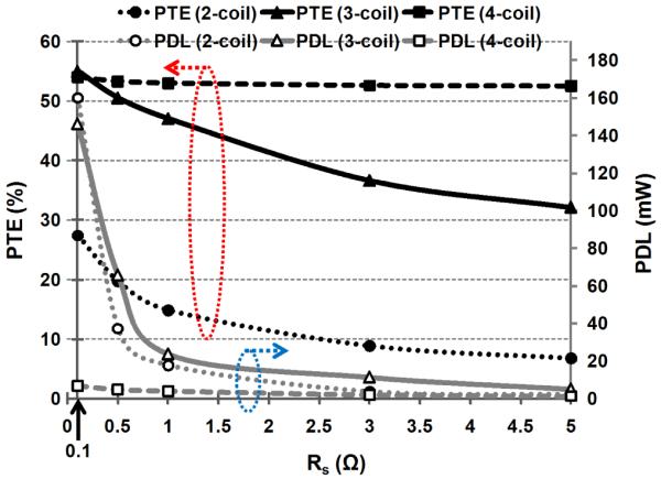
Calculated PTE and PDL vs. source resistance, Rs, for 2-, 3-, and 4-coil inductive links in the design example of Table I (Vs = 1 V, d23 = 12 cm).
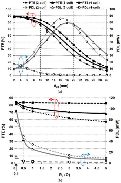
In order to compare the PTE and PDL of 2-, 3- and 4-coil links in IMD applications, where coil dimensions and coupling distances are smaller than the inductively powered neural recording system in our design example, we followed the procedure in section III on a set of inductive links to optimize them for a retinal implant [16], [39]. For this application, we chose Do3, d12, d23, d34, RL, Rs, PL equal to 10 mm, 0.1 mm, 10 mm, 0.1 mm, 100 Ω, 0.5 Ω, and 250 mW, respectively. We also assumed that all coils are PSC type with a micro-fabrication process that sets wmin and smin at 50 μm. Table II summarizes the resulting optimal geometries for Rs = 0.5 Ω, and Fig. 12a shows the calculated PTE and PDL for these inductive links vs. coupling distance, d23. At the nominal coupling distance of d23 = 10 mm, it can be seen from Table II that the PTE of the 4-coil link is only 4.9% higher than the 3-coil link. The PDL of the 3-coil link, however, is 11 times higher than the 4-coil link at the same distance. The 2-coil inductive link is also close to optimal in this condition, which is in agreement with the conclusion at the end of section II.C. At d23 = 20 mm, the difference between 4- and 3- coil PTEs increases to 7.7%, while the ratio between their PDLs reaches 192!
Table II.
Optimized PSC Geometries for IMD Applications
| Parameters | Symbols | 2-Coil | 3-Coil | 4-Coil | |
|---|---|---|---|---|---|
| L1 | Inductance (μH) | L1 | - | - | 0.12 |
| Outer diameter (mm) | D01 | - | - | 25.2 | |
| Fill factor | φ 1 | - | - | 0.24 | |
| Num. of turns | n1 | - | - | 2 | |
| Line width (mm) | W1 | - | - | 2.4 | |
| Line spacing (μm) | S1 | - | - | 150 | |
| Quality factor | Q1 | - | - | 87.4 | |
| L2 | Inductance (μH) | L2 | 1.57 | 1.22 | 0.6 |
| Outer diameter (mm) | D02 | 37 | 43 | 36.5 | |
| fill factor | φ 2 | 0.52 | 0.57 | 0.52 | |
| Num. of turns | n2 | 8 | 8 | 5 | |
| Line width (mm) | w2 | 1.45 | 1.8 | 2.4 | |
| Line spacing (μm) | S2 | 150 | 150 | 150 | |
| Quality factor | Q2 | 165 | 182 | 195 | |
| L3 | Inductance (μH) | L3 | 0.1 | 0.276 | 0.54 |
| Outer diameter (mm) | D03 | 10 | |||
| Fill factor | φ 3 | 0.26 | 0.11 | 0.15 | |
| Num. of turns | n3 | 3 | 4 | 6 | |
| Line width (mm) | w3 | 0.65 | 0.27 | 0.18 | |
| Line spacing (μm) | S3 | 50 | 50 | 50 | |
| Quality factor | Q3 | 127 | 159 | 152 | |
| L4 | Inductance (μH) | L4 | - | 0.11 | 0.16 |
| Outer diameter (mm) | D04 | - | 9.1 | 8.8 | |
| Fill factor | φ 4 | - | 0.19 | 0.25 | |
| Num. of turns | n4 | - | 3 | 4 | |
| Line width (mm) | w4 | - | 0.46 | 0.4 | |
| Line spacing (μm) | s4 | - | 50 | 50 | |
| Quality factor | Q4 | - | 129 | 154 | |
| L1 and L2 coupling distance (nun) | d12 | - | - | 0.1 | |
| L2 and L3 coupling distance (mm) | d23 | 10 | |||
| L3 and L4 coupling distance (mm) | d34 | - | 0.1 | ||
| Power transfer efficiency (%) | η | 75.7 | 78.6 | 83.5 | |
| Power delivered to load (mW) | PDL | 49.5 | 43.4 | 3.9 | |
| Nominal load (Ω) | RL | 100 | |||
| Driver output resistance (Ω) | Rs | 0.5 | |||
| Power carrier frequency (MHz) | f0 | 13.56 | |||
All coils are considered PSC type.
Grayed rows indicate the design constraints.
Fig. 12.
(a) Comparison between calculated values of the PTE and PDL vs. d23 for 2-, 3-, and 4-coil inductive links specified in Table II (Vs = 1 V, Rs = 0.5 Ω). (b) Comparison between calculated values of the PTE and PDL vs. Rs for 2-, 3-, and 4-coil inductive links for the IMD example of Table II (Vs = 1 V, d23 = 1 cm).
In Fig. 12b we have compared the calculated PTE and PDL of optimized 2-, 3- and 4-coil links vs. Rs. These curves are quite instructive by showing the designer which inductive link can provide the optimal ηov. For instance, a low power driver with Rs = 5 Ω for a low PL application favors a 4-coil inductive link to maintain high PTE despite its low PDL [17], [18]. The same 4-coil link at d23 = 20 mm will require Vs = 30 V with 100 V across a class-E PA transistor to deliver 250 mW to the load. On the other hand, a 3-coil inductive link, driven by a stronger class-E PA with Rs = 0.5 Ω, will require Vs = 1.8 V and imposes only 6 V across the PA transistor in the same conditions. It should be noted that with class-C or class-D PAs, a low-loss matching circuit can transform Rref + (R1 or R2) to the optimal load required by the PA to achieve its highest efficiency. Therefore, 3-coil inductive links can be the optimal choice for a wide range of Rs values [41].
VI. Conclusion
We have presented a design procedure to maximize the PTE in 2-, 3-, and 4-coil inductive links via a comprehensive analysis based on the reflected load theory. We have extended conventional 2-coil inductive link equations to a multi-coil arrangement to provide a platform for the analysis and design of the state-of-the-art power transmission inductive links. We have shown that the 3-coil inductive links can significantly improve the PTE and PDL, particularly at large coupling distances by transforming any arbitrary load impedance to the optimal impedance needed at the input of the inductive link. The coupling between L3 and L4 on the Rx side (k34), provides designers with a new degree of freedom for impedance transformation, which was not feasible in 2-coil links. We showed that the recently proposed 4-coil inductive links transform the load impedance to a very high reflected resistance across the driver coil, which limit the available power from source and drastically reduce PDL, particularly at large coupling distances. Furthermore, a set of 2-, 3-, and 4-coil links was optimized in a design example, modeled in HFSS, and fabricated using magnet wires and PCB. Measured results at 12 cm coupling distance showed PTE of 15%, 37%, and 35% for 2-, 3-, and 4-coil links, respectively. The 3-coil link, however, achieved a PDL of 1.5 and 59 times larger than its 2- and 4-coil counterparts, respectively.
Acknowledgments
This work was supported in part by the National Institutes of Health, NIBIB, grant 1R21EB009437-01A1, and the National Science Foundation under award ECCS-824199.
Biography

Mehdi Kiani (S’09) received his B.S. degree at Shiraz University, Shiraz, Iran and his M.S. degree at Sharif University of Technology, Tehran, Iran in 2005 and 2008 respectively. He joined GT-Bionics Lab at the Georgia Institute of Technology in 2009 where he is working towards the Ph.D. degree.

Uei-Ming Jow received the B.E. degree in electrical engineering from Tatung University, Taiwan, and the M.S. degree in electronics engineering from National Taiwan University of Science and Technology, Taiwan, in 1991 and 2001 respectively. From 2001 to 2006, he joined Industrial Technology Research Institute (ITRI) at Hsinchu, Taiwan, and worked in Electronics Research and Service Organization as an RF engineer. He was involved at the analysis and design of electromagnetic compatibility for high speed digital circuit as well as embedded RF circuits packaging technology. He is now working towards his PhD degree at the Georgia Institute of Technology. His main research interests are neural and bionic implants, integrated analog circuit design, and wireless implantable biomedical systems.

Maysam Ghovanloo (S’00–M’04–SM’10) was born in 1973 in Tehran, Iran. He received the B.S. degree in electrical engineering from the University of Tehran, Tehran, Iran, in 1994, the M.S. degree in biomedical engineering from the Amirkabir University of Technology, Tehran, Iran, in 1997, and the M.S. and Ph.D. degrees in electrical engineering from the University of Michigan, Ann Arbor, in 2003 and 2004, respectively.
From 2004 to 2007, he was an Assistant Professor in the Department of Electrical and Computer Engineering, North Carolina (NC) State University, Raleigh. In June 2007, he joined the faculty of Georgia Institute of Technology, Atlanta, where he is currently an Assistant Professor and the Founding Director of the GT-Bionics Laboratory in the School of Electrical and Computer Engineering. He has authored or coauthored more than 70 peer-reviewed conference and journal publications.
Dr. Ghovanloo is an Associate Editor of the IEEE TRANSACTIONS ON CIRCUITS AND SYSTEMS, PART-II, IEEE TRANSACTIONS ON BIOMEDICAL CIRCUITS AND SYSTEMS, and a member of the Imagers, MEMS, Medical, and Displays (IMMD) subcommittee at the International Solid-State Circuits Conference (ISSCC). He is the 2010 recipient of a CAREER award from the National Science Foundation. He has also received awards in the 40th and 41st Design Automation Conference (DAC)/ISSCC Student Design Contest in 2003 and 2004, respectively. He has organized several special sessions and was a member of Technical Review Committees for major conferences in the areas of circuits, systems, sensors, and biomedical engineering. He is a member of the Tau Beta Pi, AAAS, Sigma Xi, and the IEEE Solid-State Circuits Society, IEEE Circuits and Systems Society, and IEEE Engineering in Medicine and Biology Society.
Appendix
WWCs are often modeled as distributed RLC networks including a self-inductance in series with a resistance, both of which are in parallel with the coil parasitic capacitance [19]. The relationship between these parameters (Lself, Rwwc and CP) and the WWC geometries have been collected from various references and included in this Appendix.
Analytical expression for the self-inductance of a one turn circular conductive loop can be found from [42]
| (30) |
where μ0 and μr are the permeability of space and conductor, respectively. Do is the diameter of the loop and w is the diameter of wire. For mutual inductance, M, a wire-wound coil can be considered a set of concentric single-turn loops with various diameters, all connected in series. Using Maxwell equations, Mij between a pair of parallel single-turn circular coils at radii ri = wi/2 and rj = wj/2 can be found from [20]
| (31) |
where
| (32) |
In this equation, dij is the coupling distance between the two coils and i ≠ j. K(α) and E(α) are the complete elliptic integrals of the first and second kind, respectively [20]. Hence, the self-inductance of a WWC can be found from
| (33) |
To model the series parasitic resistance of the WWC, its DC resistance should be calculated from
| (34) |
where ρc is the resistivity of the conductive material and n is total number of turns. As the operating frequency increases, the skin effect increases the series resistance, which can be modeled as [43]
| (35) |
where
| (36) |
The parasitic capacitance between two turns of a WWC can be found from [19]
| (37) |
where ς is the thickness of the insulation layer and θe is the effective angle between turn i and turn j which is 90 degrees and s is the spacing between turns. Hence, the sum of the turn-to-turn parasitic capacitance can be approximately given by CP = 2nCturn.
Finally, considering Rwwc in series with Lself and CP in parallel with both, the quality factor of a WWC at operating frequency, ω0, can be found from [20]
| (38) |
which is valid for low frequency and small CP.
In certain applications the maximum weight of the WWC, Wmax, should also be considered in the design process. wmax, the maximum wire diameter of an n-turn WWC is related to its weight according to
| (39) |
where ρ is the density of the conducting material, which is 8.96 g/cm3 for copper. In (39) we have ignored the weight of the insulating material.
References
- [1].Clark GM. Cochlear Implants: Fundamentals and Applications. Springer-Verlag; New York: 2003. [Google Scholar]
- [2].Chen K, Yang Z, Hoang L, Weiland J, Humayun M, Liu W. An integrated 256-channel epiretinal prosthesis. IEEE J. Solid-State Circuits. 2010 Sep.45(9):1946–1956. [Google Scholar]
- [3].Harrison RR, Watkins PT, Kier RJ, Lovejoy RO, Black DJ, Greger B, Solzbacher F. A low-power integrated circuit for a wireless 100-electrode neural recording system. IEEE J. Solid-State Circuits. 2007 Jan.42(1):123–133. [Google Scholar]
- [4].Hirai J, Kim TW, Kawamura A. Study on intelligent battery charging using inductive transmission of power and information. IEEE Trans. on Power Electronics. 2000 Mar.15(2):335–345. [Google Scholar]
- [5].Finkenzeller K. RFID-Handbook. 2nd ed. Wiley; Hoboken, NJ: 2003. [Google Scholar]
- [6].Chen SCQ, Thomas V. Optimization of inductive RFID technology. Proc. IEEE Int. Symp. Electron. Environ. 2001 May;:82–87. [Google Scholar]
- [7].Lazzi G. Thermal effects bioimplants. IEEE Eng. Med. Biol. Mag. 2005 Sep.24:75–81. doi: 10.1109/memb.2005.1511503. [DOI] [PubMed] [Google Scholar]
- [8].IEEE Standard for Safety Levels With Respect to Human Exposure to Radio Frequency Electromagnetic Fields, 3 kHz to 300 GHz. IEEE Standard C95.1. 1999 [Google Scholar]
- [9].Federal Communication Commission Wireless Medical Telemetry. Online. Available: http://www.wireless.fcc.gov/services/index.htm?job=service_home&id=wireless_medical_telemetry.
- [10].Ko WH, Liang SP, Fung CDF. Design of radio-frequency powered coils for implant instruments. Med. Biol. Eng. Comput. 1977;15:634–640. doi: 10.1007/BF02457921. [DOI] [PubMed] [Google Scholar]
- [11].Donaldson NN, Perkins TA. Analysis of resonant coupled coils in the design of radio frequency transcutaneous links. Med. Biol. Eng. Comput. 1983 Sep.21(5):612–627. doi: 10.1007/BF02442388. [DOI] [PubMed] [Google Scholar]
- [12].Heetderks WJ. RF powering of millimeter and submillimeter-sized neural prosthetic implants. IEEE Trans. Biomed. Eng. 1988 May;35(5):323–327. doi: 10.1109/10.1388. [DOI] [PubMed] [Google Scholar]
- [13].Zierhofer CM, Hochmair ES. High-efficiency coupling-in sensitive transcutaneous power and data transmission via an inductive link. IEEE Trans. Biomed. Eng. 1990 July;37(7):716–722. doi: 10.1109/10.55682. [DOI] [PubMed] [Google Scholar]
- [14].Zierhofer CM, Hochmair ES. Geometric approach for coupling enhancement of magnetically coupled coils. IEEE Trans. Biomed. Eng. 1996 July;43(7):708–714. doi: 10.1109/10.503178. [DOI] [PubMed] [Google Scholar]
- [15].Neagu CR, Jansen HV, Smith A, Gardeniers JGE, Elwanspoek MC. Characterization of a planar microcoil for implantable microsystems. Sens. Actuat. A. 1997 July;62:599–611. [Google Scholar]
- [16].Kendir GA, Liu W, Wang G, Sivaprakasam M, Bashirullah R, Humayun MS, Weiland JD. An optimal design methodology for inductive power link with class-E amplifier. IEEE Trans. on Circuits and Systems I. 2005 May;52:857–866. [Google Scholar]
- [17].Harrison RR. Designing efficient inductive power links for implantable devices. IEEE International Symposium on Circuits and Systems. 2007 May;:2080–2083. [Google Scholar]
- [18].Baker MW, Sarpeshkar R. Feedback analysis and design of RF power links for low-power bionic systems. IEEE Trans. Biomed. Cir. Syst. 2007 Mar.1(1):28–38. doi: 10.1109/TBCAS.2007.893180. [DOI] [PubMed] [Google Scholar]
- [19].Yang Z, Liu W, Basham E. Inductor modeling in wireless links for implantable electronics. IEEE Trans. on Magnetics. 2007 Oct.43:3851–3860. [Google Scholar]
- [20].Jow UM, Ghovanloo M. Design and optimization of printed spiral coils for efficient transcutaneous inductive power transmission. IEEE Trans. Biomed. Cir. Syst. 2007 Sep.1:193–202. doi: 10.1109/TBCAS.2007.913130. [DOI] [PubMed] [Google Scholar]
- [21].Jow U, Ghovanloo M. Modeling and optimization of printed spiral coils in air, saline, and muscle tissue environments. IEEE Trans. Biomed. Cir. Syst. 2009 Oct.3(5):339–347. doi: 10.1109/TBCAS.2009.2025366. [DOI] [PMC free article] [PubMed] [Google Scholar]
- [22].Kurs A, Karalis A, Moffatt R, Joannopoulos JD, Fisher P, Soljacic M. Wireless power transfer via strongly coupled magnetic resonances. Science Express. 2007 July;317:83–86. doi: 10.1126/science.1143254. [DOI] [PubMed] [Google Scholar]
- [23].Cannon BL, Hoburg JF, Stancil DD, Goldstein SC. Magnetic resonant coupling as a potential means for wireless power transfer to multiple small receivers. IEEE Trans. on Power Electronics. 2009 July;24(7):1819–1825. [Google Scholar]
- [24].RamRakhyani AK, Mirabbasi S, Chiao M. Design and optimization of resonance-based efficient wireless power delivery systems for biomedical implants. IEEE Trans. Biomed. Cir. Syst. 2011 Feb.5:48–63. doi: 10.1109/TBCAS.2010.2072782. [DOI] [PubMed] [Google Scholar]
- [25].Sample AP, Meyer DA, Smith JR. Analysis, experimental results, and range adaptation of magnetically coupled resonators for wireless power transfer. IEEE Trans. Indus. Elect. 2011 Feb.58 [Google Scholar]
- [26].Karalis A, Joannopoulos J, Soljacic M. Efficient wireless non-radiative mid-range energy transfer. Annals of Physics. 2007 Apr.323:34–48. [Google Scholar]
- [27].Hamam RE, Karalis A, Joannopoulos JD, Soljacic M. Efficient weakly-radiative wireless energy transfer: An EIT-like approach. Annals of Physics. 2009 Aug;324:1783–1795. [Google Scholar]
- [28].Haus H, Huang W. Coupled-mode theory. Proc. of the IEEE. 1991 Oct.79:1505–1518. [Google Scholar]
- [29].Kiani M, Ghovanloo M. Analysis of inductive power transfer utilizing coupled-mode vs. reflected load theories. Unpublished. [Google Scholar]
- [30].Alexander CK, Sadiku M. Fundamental of Electric Circuits. 2nd ed. McGraw-Hill; New York, NY: 2004. [Google Scholar]
- [31].Lee SB, Lee HM, Kiani M, Jow U, Ghovanloo M. An inductively-powered scalable 32-channel wireless neural recording system-on-a-chip for neuroscience applications. IEEE Trans. Biomed. Cir. Syst. 2010 Dec.4(6):360–371. doi: 10.1109/TBCAS.2010.2078814. [DOI] [PMC free article] [PubMed] [Google Scholar]
- [32].Yin M, Ghovanloo M. A flexible 32-channel simultaneous wireless neural recording system with adjustable resolution. Digest of technical papers IEEE Intl. Solid State Cir. Conf. 2009 Feb.:432–433. [Google Scholar]
- [33].Yin M, Ghovanloo M. A low-noise clockless simultaneous 32-channel wireless neural recording system with adjustable resolution. Analog Integrated Circuits Signal Proc. 2010 Nov.66(3) [Google Scholar]
- [34].Chae MS, Yang Z, Yuce MR, Hoang L, Liu W. A 128-channel 6 mW wireless neural recording IC with spike feature extraction and UWB transmitter. IEEE Trans. on Neural Sys. Rehab. Eng. 2009 Aug.17(4):312–321. doi: 10.1109/TNSRE.2009.2021607. [DOI] [PubMed] [Google Scholar]
- [35].Miranda H, Gilja V, Chestek CA, Shenoy KV, Meng TH. HermesD: a high-rate long-range wireless transmission system for simultaneous multichannel neural recording applications. IEEE Trans. Biomed. Cir. Syst. 2010 June;4(3):181–191. doi: 10.1109/TBCAS.2010.2044573. [DOI] [PubMed] [Google Scholar]
- [36].Rizk M, Bossetti CA, Jochum TA, Callender SH, Nicolelis MAL, Turner DA, Wolf PD. A fully implantable 96-channel neural data acquisition system. J. Neural Eng. 2009 Apr.6(2) doi: 10.1088/1741-2560/6/2/026002. art. 026002. [DOI] [PMC free article] [PubMed] [Google Scholar]
- [37].Manns JR, Howard MW, Eichenbaum H. Gradual changes in hippocampal activity support remembering the order of events. Neuron. 2007 Nov.56(3):530–540. doi: 10.1016/j.neuron.2007.08.017. [DOI] [PMC free article] [PubMed] [Google Scholar]
- [38].Pozar DM. Microwave Engineering. 2nd ed. Wiley; New York: 1998. ch. 4. [Google Scholar]
- [39].Shire DB, Kelly SK, Chen J, Doyle P, Gingerich MD, Cogan SF, Drohan WA, Mendoza O, Theogarajan L, Wyatt JL, Rizzo JF. Development and implantation of a minimally invasive wireless subretinal neurostimulator. IEEE Trans. Biomed. Eng. 2009 Oct.56(10):2502–2511. doi: 10.1109/TBME.2009.2021401. [DOI] [PMC free article] [PubMed] [Google Scholar]
- [40].Kazimierczuk MK, Czarkowski D. Resonant Power Converters. Wiley-Interscience; NY: 1995. [Google Scholar]
- [41].Kiani M, Ghovanloo M. An RFID-based closed loop wireless power transmission system for biomedical applications. IEEE Trans. Cir. Syst. II. 2010 Apr.57(4):260–264. doi: 10.1109/TCSII.2010.2043470. [DOI] [PMC free article] [PubMed] [Google Scholar]
- [42].Sadiku N. Elements of Electromagnetics. Sounders College Press; Orlando, FL: 1994. [Google Scholar]
- [43].Wheeler HAA. Formulas for the skin effect. Proc. of the IRE. 1942 Sep.30(9):412–424. [Google Scholar]


