Abstract
Conductive-probe atomic force microscopy (CP-AFM) measurements reveal the existence of a conductive channel at the interface between p-type hydrogenated amorphous silicon (a-Si:H) and n-type crystalline silicon (c-Si) as well as at the interface between n-type a-Si:H and p-type c-Si. This is in good agreement with planar conductance measurements that show a large interface conductance. It is demonstrated that these features are related to the existence of a strong inversion layer of holes at the c-Si surface of (p) a-Si:H/(n) c-Si structures, and to a strong inversion layer of electrons at the c-Si surface of (n) a-Si:H/(p) c-Si heterojunctions. These are intimately related to the band offsets, which allows us to determine these parameters with good precision.
Introduction
In the field of silicon solar cells, recent progress has been achieved in two directions: silicon heterojunctions and silicon nanowires. These two topics are briefly addressed here and we show some new characterization results that use conductive-probe atomic force microscopy (CP-AFM) measurements.
Silicon heterojunctions are formed between crystalline silicon (c-Si) and hydrogenated amorphous silicon (a-Si:H). Solar cell efficiencies of up to 23% have been demonstrated on high quality n-type c-Si wafers with layers of p-type a-Si:H deposited at the front (as the emitter) and n-type a-Si:H deposited at the back (as the back surface field), respectively [1]. Since transport properties are quite poor in a-Si:H due to the large amount of defects and band gap states and low carrier mobilities, the doped a-Si:H layers are used to form the junctions, but their thickness has to be kept very low. The front a-Si:H layer has to be very thin in order to minimize absorption of incoming photons and to privilege absorption in c-Si. One key feature of the Si heterojunctions is the very good passivation property of the c-Si surface by a-Si:H. This is even improved by inserting a thin undoped a-Si:H layer (so-called "intrinsic" layer, which leads to the "HIT"-heterojunction with intrinsic thin layer denomination [2]). This limits interface recombination and leads to very high open circuit voltages [3]. Band offsets between a-Si:H and c-Si also play a crucial role because they determine the band bending, which influences the carrier collection. We here demonstrate the existence of a conduction channel along both the (n) a-Si:H/(p) c-Si and the (p) a-Si:H/(n) c-Si interfaces from direct CP-AFM measurements performed on cleaved sections of solar cells. We show from additional planar conductance measurements and simulations that these are related to strong inversion regions at the interfaces. From the temperature dependence, we determine the values of band offsets.
Experimental details
Solar cell structure
A typical solar cell structure based on a-Si:H/c-Si heterojunctions formed with n-type c-Si is presented in Figure 1. A similar structure stands for p-type c-Si, replacing the n-type a-Si:H by p-type a-Si:H and vice versa. For n-type c-Si, we used Float Zone, n-type c-Si wafers, 〈100〉 oriented, with resistivity: ρ = 1-5 Ω cm, and thickness: W = 300 μm. For the p-type c-Si, we used Czochralski (CZ) c-Si wafers, 〈100〉 oriented, with resistivity: ρ = 14-22 Ω cm, and thickness: W = 300 μm. We used indium tin oxide (ITO) as the front transparent conductive oxide (TCO), and aluminum as the back metal contact. The a-Si:H layers were deposited at Ecole Polytechnique in a radio frequency (13.56 MHz) plasma-enhanced chemical vapor deposition (PECVD) reactor at a substrate temperature of 200°C. Spectroscopic ellipsometry measurements and modeling were used to check that the deposited silicon thin layers were truly amorphous, and that no epitaxial growth occurred on the c-Si substrate.
Figure 1.
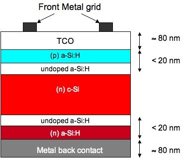
Cross-section of a silicon heterojunction solar cell on n-type c-Si.
CP-AFM
CP-AFM measurements were carried out using two different setups (i) in Ioffe Physical-technical Institute (NT-MDT Ntegra Aura) and (ii) in Laboratoire de Génie Électrique de Paris (Digital Instruments Nanoscope IIIa Multimode AFM with the RESISCOPE extension [4]). These setups allow one to apply a stable DC bias voltage to the device and to measure the resulting current flowing through the tip as the sample surface is scanned in contact mode. Schematic AFM setup is shown in Figure 2. In both measurements diamond-coated conductive probes made of silicon were used, the contact interaction force being in the range 100-500 nN. With the help of this technique one can simultaneously examine on the sample cleavages the surface topography and conductive properties of the layers constituting the solar cells. Note that, due to different softwares, the first setup provides images with current values (current flowing through the tip), while the second one provides resistance values, the resistance being defined as the ratio of the applied voltage to the measured current.
Figure 2.

Sketch of the CP-AFM measurements; left: setup at LGEP with the resiscope extension; right: detail of the sample configuration and biasing.
For these CP-AFM measurements, the normal solar cell structure was replaced by a simpler symmetric configuration, see Figure 3a, where the same a-Si:H layer was deposited on both sides of the c-Si wafer. Then ITO electrodes were deposited on top of both sides of the wafer, before the sample was cleaved. Some tests were also performed with aluminum instead of ITO as electrodes. The obtained CP-AFM results were globally the same. However, aluminum electrodes formed high ridges at the cleaved edge and their cross-section were poorly conductive due to strong oxidation of aluminum, what induced some problems in AFM imaging. Therefore, here we focus on samples with ITO on both sides. Thus, cleaved sections of ITO/(n) a-Si:H/(p) c-Si/ITO and ITO/(p) a-Si:H/(n) c-Si/ITO samples with different thicknesses of the a-Si:H layer (20, 100, 300 nm) were investigated.
Figure 3.
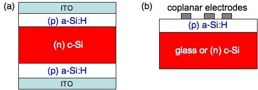
Sketch of the samples prepared for (a) CP-AFM measurements and (b) planar conductance measurements.
Planar conductance
The sample structure for these measurements is shown in Figure 3b for p-doped a-Si:H. The a-Si:H layer was deposited in the same run on both n-type c-Si and glass (Corning 1737). Top coplanar aluminum electrodes were then deposited on the top of a-Si:H. We measured the DC current, I, resulting from application of a DC bias, V, between two adjacent electrodes. We had several electrode designs with various gap distances between them. We checked that the current scaled with the inter-electrode gap distance. We also checked that the current was linearly dependent on the DC voltage, so that we defined the conductance G = I/V. This was then measured as a function of temperature between 150 and 300 K in a cryostat chamber pumped down to 10-5 mbar.
The same kind of measurements were also performed on series of samples with n-doped a-Si:H deposited onto p-type c-Si and glass.
Results and discussion
In Figure 4a,b,c, an example of topography and current images for two different biases, is presented for a (p) a-Si:H/(n) c-Si junction. At positive bias applied to the sample, conductive regions appear light in the current images, while for negative bias they appear dark. The current images clearly reveal a conductive interface layer between the c-Si substrate and the a-Si:H film. This layer is more conductive than both the c-Si and a-Si:H regions. This conductive interface layer was well observed on all samples for both (p) a-Si:H/(n) c-Si and (n) a-Si:H/(p) c-Si heterointerfaces whatever the a-Si:H layer thickness is. It is worth to note that the conductive layer is not an artifact that could come from the surface roughness. It can be clearly seen when current images are compared with the topography one. There exists one distinct boundary between the a-Si:H layer and c-Si wafer, and the detected conductive channel lies within c-Si substrate.
Figure 4.
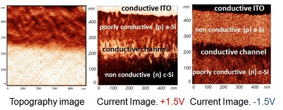
AFM pictures taken on a cleaved section of an ITO/(p) a-Si:H/(n) c-Si/ITO sample. Left: topography; middle: current image taken at an applied bias of +1.5 V. Right: current image taken at an applied bias of -1.5 V. Typical roughness was less than 5 nm. On the topographical image, the change in height from the dark top region to the light bottom region was of the order of 2 nm. In the current images, the current values ranged from 60 pA to 17 nA.
However, the quantitative results of the interface layer conductivity deduced from CP-AFM measurements have to be considered carefully. Indeed, the reliability of the latter is affected by the quality and nature of the contact between the conductive tip and the sample surface. The sample surface roughness, the AFM tip radius, shape and pressure are well-known factors driving local electrical measurements. Moreover, surface states can induce additional band bending at the tip-surface junction modifying significantly the conductance values [5]. The CP-AFM scanning measurements can also be influenced by the oxidation process after cleaving the sample and the presence of a water meniscus between the tip and the surface that can also lead to tip-induced oxidation or trapping of carriers in localized states [6,7]. The contact between the tip and the cleaved surface can behave as a metal-oxide interface that then determines the current flowing through the tip.
In order to minimize the effects of surface oxide and surface states, CP-AFM measurements were performed at LGEP under nitrogen atmosphere immediately after having dipped the sample in an HF solution. This treatment is known to passivate the silicon surface by reducing the density of silicon dangling bonds, thus minimizing the potential effect of surface states on the surface band bending. Figure 5 illustrates an example of topographical and electrical image of the cleaved section obtained under these conditions with, from top to bottom, the n-type a-Si:H layer (= 300 nm) and the p-type c-Si substrate. Contrary to Figure 4, the ITO contact is not observed since it has been partially removed after the HF dip. Compared to results of Figure 4, with the improved measurement procedure, a conductive channel at the (n) a-Si:H/(p) c-Si interface is even more clearly observed. The topographic and electrical profiles along the heterointerface presented on Figure 6 show a flat cleaved surface and a higher electrical contrast between the conductive channel and both the a-Si:H layer and the c-Si substrate. In addition, the electrical image in the c-Si also shows a region with increasing conductivity of about 1 μm width when sweeping away from the a-Si:H/c-Si interface. This can be linked to the depleted space charge region in the low-doped (p) c-Si (Na < 1015 cm-3), which has a width close to 1 μm.
Figure 5.
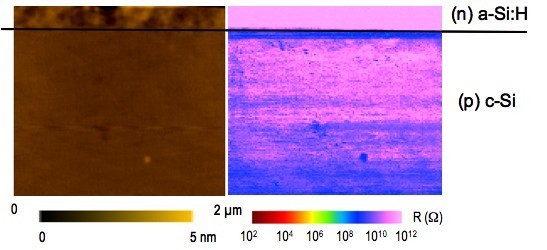
Topography and electrical image obtained after HF dip at the cleaved section of an (n) a-Si:H/(p) c-Si heterojunction. Left: topography; right: resistance image.
Figure 6.
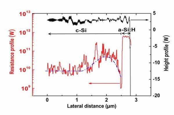
Profile of local resistance across the (n) a-Si:H/(p) c-Si interface corresponding to Figure 5.
The existence of an interface conductive channel has also been evidenced by the planar conductance measurements. Indeed, it was shown that the planar conductance was orders of magnitude larger for the samples deposited on c-Si substrates (both n- and p-type) than that measured on the a-Si:H layer deposited in the same run on glass substrates. Activation energy of the conductance for the samples deposited on glass was found equal to about 0.35 and 0.2 eV for the (p) a-Si:H and (n) a-Si:H layers, respectively [8,9]. These are typical values for doped a-Si:H. The conductance for samples deposited on c-Si had much lower activation energy, as can be seen in Figure 7. This high planar conductance measured on the samples deposited on c-Si is in very good agreement with the presence of the conducting channel revealed by our CP-AFM measurements.
Figure 7.
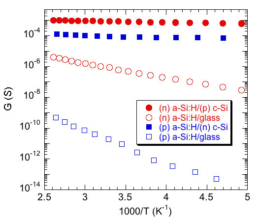
Arrhenius plots of the planar conductance measured on various samples. Red circles for (n) a-Si:H, blue squares for (p) a-Si:H, full symbols for layers deposited on c-Si wafer (on opposite doping type with respect to the deposited a-Si:H layer), open symbols for layers deposited on glass.
We attribute this thin conductive interface channel along with the low conductance activation energy to a strong inversion layer at the c-Si surface that is related to the band offset at the heterojunction.
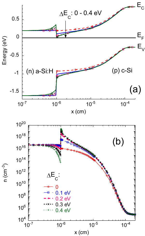
In order to further demonstrate the existence of the strong interface inversion layer and the related contribution to the conductance, we used the AFORS-HET software [10] to evaluate the free carrier profiles. We introduced the density of states (DOS) typical for n-type a-Si:H (band gap Eg = 1.75 eV) consisting of two exponential band tails with characteristic energies kBTC and kBTV of 0.055 and 0.12 eV for the conduction and valence band, respectively, and with a pre-exponential factor of 2 × 1021 cm-3 eV-1, and two Gaussian deep defect distributions of donor and acceptor nature being located at 0.58 and 0.78 eV above the top of the valence band, respectively, with a maximum value of 8.7 × 1019 cm-3 eV-1 and a standard deviation of 0.23 eV. A doping density of Nd = 5.34 × 1019 cm-3 was also introduced, setting the Fermi level EF at 0.2 eV below the conduction band at 300 K, as suggested from the activation energy of the conductance data measured on (n) a-Si:H samples deposited on glass. The doping density in the crystalline silicon was set at Na = 7 × 1014 cm-3, as found from capacitance versus bias measurements [11], and in agreement with the resistivity of our CZ c-Si p-type wafers.
Figure 8a,b shows the calculated band diagram and the electron concentration profile for various values of the conduction band offset ΔEC = ECa-Si:H - ECc-Si, respectively. An inversion layer is indeed clearly seen in the interface region of c-Si when sticking increase of electron concentration with ΔEC is observed. On the contrary, increasing ΔEC leads to a stronger electron depletion in (n) a-Si:H close to the interface due to a stronger band bending.
Figure 8.
Modeling of the (n) a-Si:H/(p) c-Si heterojunction at equilibrium for various values of the conduction band offset. (a) band diagram, and (b) free electron concentration profile.
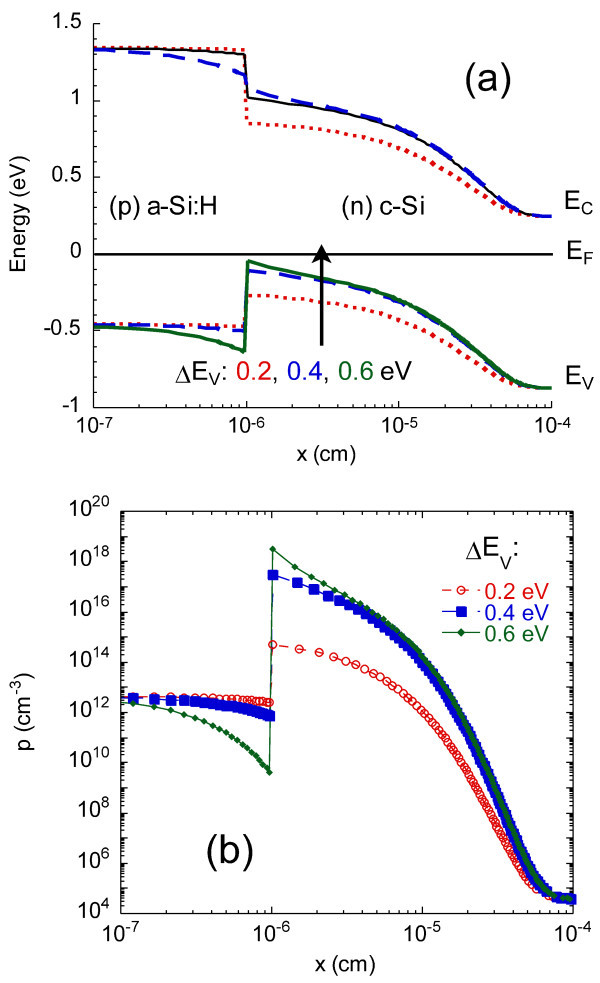
Similar simulations were performed for the (p) a-Si:H/(n) c-Si heterojunction. The band gap of a-Si:H also was taken at Eg = 1.75 eV, and the position of the Fermi level was fixed at 0.45 eV, which is a reasonable value for p-type a-Si:H, in agreement with our conductivity measurements. After having introduced the a-Si:H parameters, we combined the a-Si:H layer with an n-type c-Si substrate with Nd = 2 × 1015 cm-3 (corresponding to the resistivity value) to simulate the (p) a-Si:H/(n) c-Si heterojunction. Calculated band diagram and evaluated hole concentration profiles for different values of valence band offset ΔEV = EVc-Si - EVa-Si:H are shown in Figure 9a,b, respectively. Drastic increase of hole concentration is observed in (n) c-Si layer near the interface for increasing values of band offset, with the appearance of a strong inversion layer for ΔEV > 0.2 eV. Thus, simulations of both (n) a-Si:H/(p) c-Si and (p) a-Si:H/(n) c-Si heterojunctions show the appearance of a strong inversion interface region above a given value of band offset. The planar conductance can be related to the carrier density profile. Indeed, the conductance of the strong inversion channel can be written
Figure 9.
Modeling of the (p) a-Si:H/(n) c-Si heterojunction at equilibrium for various values of the valence band offset. (a) band diagram, and (b) free hole concentration profile.
| (1) |
where q is the elementary charge, h the length of the coplanar electrodes, L the gap between them, μ the mobility of the carriers in the strong inversion region, and N the sheet carrier density, i.e., the integral over the c-Si thickness of the carrier concentration. Carriers to be considered are the electrons for the (n) a-Si:H/(p) c-Si interface and the holes for the (p) a-Si:H/(n) c-Si interface. We calculated the values of N as a function of the band offset and of the temperature. We thus were able to compute the planar conductance and compare it to the experimental data. This proved to be a very precise way to determine the band offsets in the (n) a-Si:H/(p) c-Si system [12], where a value of ΔEC = 0.15 eV was found. In the (p) a-Si:H/(n) c-Si system, the measured resistance profile was compared to the calculated resistivity profile across the heterojunction. Both profiles have very similar shapes, and the thickness of the strong inversion layer is of the same order of magnitude (50-100 nm). Further analysis of the CP-AFM measurements shows that a strong inversion layer only exists if the valence band offset is large enough, ΔEV > 0.25 eV [13]. A more detailed theoretical and modeling study including the effect of temperature dependence of the band gaps and of the DOS parameters in a-Si:H is under way. It confirms our previous determination of conduction band offset and indicates that the value of valence band offset that best reproduces our experimental data is around ΔEV = 0.4 eV.
Conclusion
Silicon heterojunctions were characterized by the CP-AFM technique. A conductive channel between a-Si:H layer and c-Si substrate was detected in both (n) a-Si:H/(p) c-Si and (p) a-Si:H/(n) c-Si heterostructures. This conductive channel was attributed to the existence of a strong inversion layer that was also suggested by planar conductance measurements. The existence of this layer can be explained by relatively large band offsets at the heterojunction, as we demonstrated by numerical calculations of the carrier concentration profiles. Comparison with our experimental data allowed us to deduce values of the conduction and valence band offsets.
Abbreviations
CP-AFM: conductive-probe atomic force microscopy; CZ: Czochralski; DOS: density of states; ITO: indium tin oxide; PECVD: plasma-enhanced chemical vapor deposition; TCO: transparent conductive oxide.
Competing interests
The authors declare that they have no competing interests.
Authors' contributions
PRIC and ML deposited the samples. JA, AVA, and EVG carried out CP-AFM measurements. WF carried out planar conductance measurements. ASG and OAM performed modeling. MEGF and EIT participated in the analysis and guidance of the study. JPK supervised the study, participated in the analysis of the results, and drafted the manuscript. All authors read and approved the manuscript.
Contributor Information
Jean-Paul Kleider, Email: jean-paul.kleider@lgep.supelec.fr.
Jose Alvarez, Email: jose.alvarez@lgep.supelec.fr.
Alexander Vitalievitch Ankudinov, Email: alexander.ankudinov@mail.ioffe.ru.
Alexander Sergeevitch Gudovskikh, Email: gudovskikh@edu.ioffe.ru.
Ekaterina Vladimirovna Gushchina, Email: katgushch@yandex.ru.
Martin Labrune, Email: martin.labrune@polytechnique.edu.
Olga Alexandrovna Maslova, Email: olga.maslova@lgep.supelec.fr.
Wilfried Favre, Email: wilfried.favre@lgep.supelec.fr.
Marie-Estelle Gueunier-Farret, Email: farret@lgep.supelec.fr.
Pere Roca i Cabarrocas, Email: pere.roca@polytechnique.edu.
Eugene Ivanovitch Terukov, Email: eug.terukov@mail.ioffe.ru.
Acknowledgements
This study was partly supported by European Community's Seventh Framework Programme (FP7/2007-2013) under Grant agreement no. 211821 (HETSI project), by OSEO's Solar Nanocrystal project as well as by CNRS and the Russian Foundation for Basic Research in the framework of a joint Russian-French project (07-08-92163), and by the Programme of Fundamental Research of Russian Academy of Sciences (Programme No. 27). Two of the authors, W. Favre and O.A. Maslova, would like to thank ADEME and SUPELEC, and the French embassy in Russia, respectively, for their grants.
References
- Mishima T, Taguchi M, Sakata H, Maruyama E. Development status of high-efficiency HIT solar cells. Sol Energy Mater Sol Cells. 2011;95:18. doi: 10.1016/j.solmat.2010.04.030. [DOI] [Google Scholar]
- Tanaka M, Taguchi M, Matsuyama T, Sawada T, Tsuda S, Nakano S, Hanafusa H, Kuwano Y. Development of New a-Si/c-Si Heterojunction Solar Cells: ACJ-HIT (Artificially Constructed Junction-Heterojunction with Intrinsic Thin-Layer) Jpn J Appl Phys. 1992;31:3518. doi: 10.1143/JJAP.31.3518. [DOI] [Google Scholar]
- Taguchi M, Tsunomura Y, Inoue H, Taira S, Nakashima T, Baba T, Sakata H, Maruyama E. High efficiency HIT solar cell on thin (< 100 μm ) silicon wafer. Proceedings of the 24th EPVSEC; Hamburg, Germany. 2009. pp. 1690–1693.
- Houze F, Schneegans O, Boyer L. Imaging the local electrical properties of metal surfaces by atomic force microscopy with conducting probes. Appl Phys Lett. 1996;69:1975. doi: 10.1063/1.117179. [DOI] [Google Scholar]
- Eyben P, Vandervorst W, Alvarez D, Xu M, Fouchier M. In: Scanning Probe Microscopy. Kalinin S, Gruverman A, editor. New York: Springer; 2007. Probing Semiconductor Technology and Devices with Scanning Spreading Resistance Microscopy; pp. 31–88. full_text. [Google Scholar]
- Kleider JP, Longeaud C, Bruggemann R, Houze F. Electronic and topographic properties of amorphous and microcrystalline silicon thin films. Thin Solid Films. 2001;383:57. doi: 10.1016/S0040-6090(00)01614-X. [DOI] [Google Scholar]
- Rezek B, Mates T, Sipek E, Stuchlik J, Fejfar A, Kocka J. Influence of combined AFM/current measurement on local electronic properties of silicon thin films. J Non-Cryst Solids. 2002;299-302:360. doi: 10.1016/S0022-3093(01)01012-2. [DOI] [Google Scholar]
- Kleider JP, Soro YM, Chouffot R, Gudovskikh AS, Rocai Cabarrocas P, Damon-Lacoste J, Eon D, Ribeyron P-J. High interfacial conductivity at amorphous silicon/crystalline silicon heterojunctions. J Non-Cryst Solids. 2008;354:2641. doi: 10.1016/j.jnoncrysol.2007.09.087. [DOI] [Google Scholar]
- Favre W, Labrune M, Dadouche F, Gudovskikh AS, Rocai Cabarrocas P, Kleider JP. Study of the interfacial properties of amorphous silicon/n-type crystalline silicon heterojunction through static planar conductance measurements. Phys Status Solidi C. 2010;7:1037. [Google Scholar]
- Stangl R, Kriegel M, Schmidt M. AFORS-HET, Version 2.2, a numerical computer program for simulation of heterojunction solar cells and measurements. Proceedings of the 4th World Conference on Photovoltaic Energy Conversion; Hawaii, USA. 2006. pp. 1350–1353.
- Gudovskikh AS, Ibrahim S, Kleider JP, Damon-Lacoste J, Rocai Cabarrocas P, Veschetti Y, Ribeyron PJ. Determination of band offsets in a-Si:H/c-Si heterojunctions from capacitance-voltage measurements: Capabilities and limits. Thin Solid Films. 2007;515:7481. doi: 10.1016/j.tsf.2006.11.198. [DOI] [Google Scholar]
- Kleider JP, Gudovskikh AS, Rocai Cabarrocas P. Determination of the conduction band offset between hydrogenated amorphous silicon and crystalline silicon from surface inversion layer conductance measurements. Appl Phys Lett. 2008;92:162101. doi: 10.1063/1.2907695. [DOI] [Google Scholar]
- Maslova OA, Alvarez J, Gushina EV, Favre W, Gueunier-Farret ME, Gudovskikh AS, Ankudinov AV, Terukov EI, Kleider JP. Observation by conductive-probe atomic force microscopy of strongly inverted surface layers at the hydrogenated amorphous silicon/crystalline silicon heterojunctions. Appl Phys Lett. 2008;97:252110. doi: 10.1063/1.3525166. [DOI] [Google Scholar]


