Abstract
Silicon, germanium, and related alloys, which provide the leading materials platform of electronics, are extremely inefficient light emitters because of the indirect nature of their fundamental energy bandgap. This basic materials property has so far hindered the development of group-IV photonic active devices, including diode lasers, thereby significantly limiting our ability to integrate electronic and photonic functionalities at the chip level. Here we show that Ge nanomembranes (i.e., single-crystal sheets no more than a few tens of nanometers thick) can be used to overcome this materials limitation. Theoretical studies have predicted that tensile strain in Ge lowers the direct energy bandgap relative to the indirect one. We demonstrate that mechanically stressed nanomembranes allow for the introduction of sufficient biaxial tensile strain to transform Ge into a direct-bandgap material with strongly enhanced light-emission efficiency, capable of supporting population inversion as required for providing optical gain.
Keywords: luminescence, strain engineering, band structure
The controlled introduction of strain in semiconductors offers an important degree of freedom for basic materials studies as well as advanced device engineering. Strain in a crystalline solid modifies the lattice constants and reduces the crystal symmetry, leading to significant shifts in the energy band edges, often accompanied by a splitting of degenerate states, and to changes in the relevant effective masses. These effects can be used, for example, to produce a desired band offset between different materials, to increase mobility in electronic devices (1), and to reduce the transparency carrier density and increase the differential gain in diode lasers (2, 3). Traditionally, the use of strain for these and similar applications has relied on the epitaxial growth of overlayers with sufficiently small thicknesses (to avoid dislocation formation; ref. 4) on lattice mismatched substrates. More recently, semiconductor nanomembranes (NMs) have emerged as a materials platform offering unique opportunities for strain engineering (5–8), both through spontaneous elastic strain sharing upon NM release and through the external application of mechanical stress. In the present work, this basic platform is applied to a major outstanding goal of semiconductor optoelectronics, namely, the demonstration of practical silicon-compatible light sources. In particular, we show that biaxial tensile strain in mechanically stressed Ge NMs can be used to transform Ge into a direct-bandgap material with strongly enhanced radiative efficiency and capable of supporting population inversion, as required for laser action. Importantly, these strained Ge NMs are highly luminescent already at room temperature, are suitable for light emission via electrical injection, and can be fully integrated with complementary-metal-oxide-semiconductor (CMOS) electronic devices using microelectromechanical-systems (MEMS) technology. Therefore, unlike existing approaches, strained Ge NMs meet all the key requirements of group-IV photonic active materials.
It is established doctrine that Si, Ge, and related alloys are not suitable to the development of light-emitting diodes and lasers based on traditional approaches, because their indirect energy bandgap results in exceedingly low radiative recombination efficiency. This issue represents the key factor currently limiting the integration of electronics and photonics on a CMOS-compatible platform, and as a result, a wide range of ideas and technologies is being explored to address it. Here we consider the use of Ge under biaxial tensile strain ε—i.e., with the in-plane lattice constant a dilated by the amount Δa = εa. Tensile strain has been theoretically predicted to lower the conduction band edge at the direct (Γ) point relative to the L valleys (i.e., the conduction-band minima in the <111> directions of the crystal, which determine the fundamental, but indirect, gap at zero strain, Eg = 0.66 eV at 300 K), while the overall bandgap energy correspondingly decreases (9–14). In the presence of electrical or optical pumping, a substantial population of electrons at the Γ minimum can therefore be established in sufficiently tensilely strained Ge, thereby increasing the light-emission efficiency and enabling optical gain. The fundamental bandgap even becomes direct for biaxial strains in excess of a certain value, which is generally computed to be less than 2% (9–14). Furthermore, according to the calculations of ref. 12, population inversion and laser action in undoped Ge can already be achieved at a lower biaxial tensile strain of about 1.5%.
The introduction of such levels of biaxial tensile strain in high-quality Ge has so far remained inaccessible. The traditional approach of heteroepitaxy is in this case problematic, as compatible and commonly used substrates such as Si or SiGe have smaller in-plane lattice constants, and therefore under pseudomorphic-growth conditions produce compressively strained Ge epilayers. Tensilely strained Ge can be grown on InGaAs templates, as shown in a recent report of strain-enhanced photoluminescence at cryogenic temperatures (15); however, this approach is not compatible with Si-based CMOS technology. Similarly, SiGeSn has been proposed as a suitable growth template for the same purpose (10, 16), but its epitaxy is quite challenging and still under development. Tensile strain can also be introduced in plastically relaxed Ge films grown on Si by using an annealing process to take advantage of the difference in thermal-expansion coefficients between Si and Ge (11). Optically pumped lasing has, in fact, been recently demonstrated with such Ge-on-Si films (17). Because the maximum Ge strain that can be introduced in this manner is quite small (0.25%), population inversion could only be achieved using highly degenerate n-type doping to raise the electronic quasi-Fermi level, a feature that will be quite problematic for the development of electrically driven diode lasers (the ultimate goal of group-IV photonics).
An alternative way to introduce strain in crystalline materials in a controllable fashion is the external application of mechanical stress. This approach is quite flexible, and in fact historically has provided one of the earliest means used to investigate the effect of strain on the electronic and optical properties of semiconductors (18). Furthermore, the external application of stress allows tailoring the materials properties after sample preparation, which is attractive for both basic studies and device applications. At the same time, this approach has the important limitation that, as long as bulk samples are employed, only small amounts of tensile strain can be produced before the onset of significant extended-defect formation (19). This limitation is clearly illustrated in recent attempts to study direct-bandgap light emission from mechanically stressed bulk Ge (20, 21), where maximum tensile strains of only 0.6% or less could be introduced, limited by sample debonding or fracture.
Ge NMs, which are based on a fabrication technology that has been developed in recent years for a wide range of applications (5–8, 22–28), offer another perspective. With this technology, free-standing NMs are produced that can be readily transferred and bonded onto a flexible host substrate and then mechanically stretched. Furthermore, their characteristic thicknesses of only a few tens of nanometers lead to substantially larger strain thresholds for plastic deformation and for cracking than in bulk materials. Specifically, because the amount of strain energy stored in the NM is directly proportional to its thickness, when very thin compared to the substrate, the NM contains insufficient strain energy to drive defect formation (19). NMs therefore represent the ideal materials platform for strain engineering studies and applications in which strain is a controlling factor. Here, biaxial tensile strain is introduced in mechanically stressed Ge NMs to modify their band structure, leading to a substantial increase and a red shift in room-temperature luminescence. A quantitative analysis of the emission spectra shows that under high strain the NMs are already pumped above optical transparency. Furthermore, for the thinnest (24-nm) NMs tested, the maximum strain levels obtained are above the predicted onset of direct-bandgap behavior.
Results and Discussion
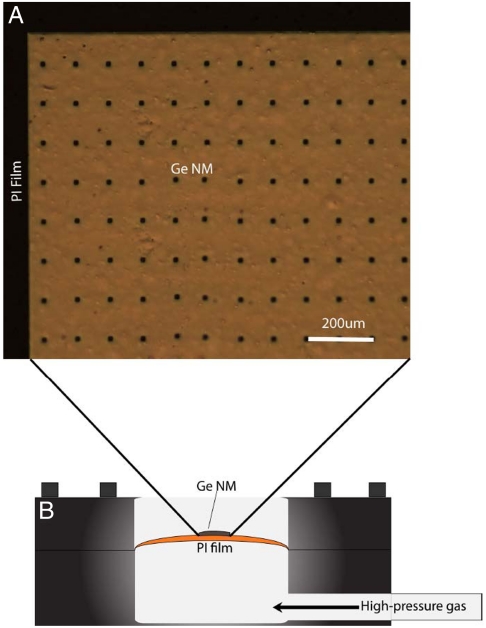
The free-standing NMs are fabricated by releasing the top Ge layer of (001) Ge-on-insulator (GOI) substrates, using a wet etch to dissolve the underlying buried oxide. The resulting NMs, which are nominally undoped, are subsequently transferred and bonded onto 125-μm-thick, flexible polyimide (PI) films. A top-view optical micrograph of a Ge NM bonded on a PI film is shown in Fig. 1A. In the strain-resolved optical measurements described in the following, the PI film is used to seal an otherwise rigid cavity that is then filled with high-pressure gas, so that the film and the attached NM can be mechanically stretched in a highly controllable fashion. A schematic diagram of the sample holder is shown in Fig. 1B. Because in this setup the NM effectively lies on the surface of an expanding sphere of plastically deforming PI, the resulting strains are biaxial and depend solely on the substrate curvature. The strain in the plane of the NMs is measured as a function of applied stress (i.e., gas pressure) via Raman spectroscopy. The NM light-emission properties are investigated via room-temperature photoluminescence (PL).
Fig. 1.
Ge NMs and schematic sample mount. (A) Optical micrograph of a Ge NM bonded on a PI film. The array of etchant access holes used in the release process (see Materials and Methods) is clearly visible. (B) Diagram showing the sample mount and the location of the NM with respect to the applied high-pressure gas.
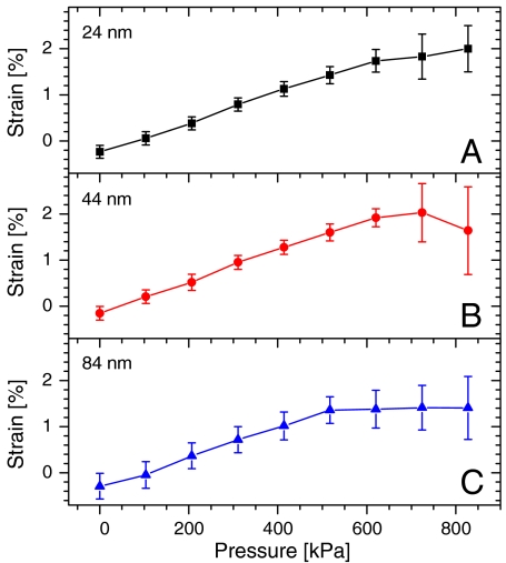
The stress/strain curves of three representative NMs, 24-, 44-, and 84-nm thick, are plotted in Fig. 2. The small amount of compressive strain observed at zero pressure is attributed to PI-substrate curing effects (see Materials and Methods). As the sample mount is pressurized, the measured biaxial tensile strain (averaged over several random sites on the NM) initially increases linearly with the applied stress, as expected in the elastic region of the stress/strain curve in the absence of delamination. Beyond a certain stress, the stress/strain relationship is no longer linear, owing to the formation of cracks in the NM, which are visible in the Raman microscope, and which produce strain relaxation via plastic deformation in their immediate vicinity. As the pressure is further increased, more and more of the NM area no longer contributes to the maximum strain, leading to a saturation of the average strain and an increase in its standard deviation (indicated by the error bars in the figure). The implication, of course, is that we also have an increasing range of bandgaps contributing to the light emission as we go beyond the linear region of the stress/strain curve.
Fig. 2.
Stress/strain curves of three Ge NMs of different thicknesses. NM strain versus gas pressure in the sample mount (Fig. 1B), as measured via Raman spectroscopy for (A) 24-, (B) 44-, and (C) 84-nm-thick Ge NMs.
As mentioned earlier, for the same reasons that very little strain can be induced in bulk samples, the degree of crack formation at a given stress (which ultimately limits the maximum average strain) increases with membrane thickness. Specifically, for the 84-nm-thick NM, the measured area-averaged strain saturates at approximately 1.4% above approximately 500 kPa, as shown in Fig. 2C. For the 24-nm-thick NM, the area-averaged tensile strain continues to increase linearly with pressure up to a value of 2.0% at 700–800 kPa. Results for the 44-nm-thick NM are consistent, with the area-averaged strain reaching a peak value of about 2.0% at a pressure of approximately 700 kPa and then leveling off. The comparison between the traces in Fig. 2 therefore highlights the importance of nanoscale thicknesses to obtain the desired large amounts of tensile strain.
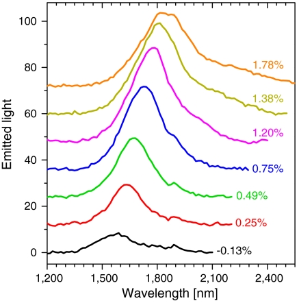
Exemplary room-temperature PL spectra obtained from a 40-nm-thick NM at different strains are shown in Fig. 3. In these measurements, the applied stress was kept below the point of plastic deformation (ca. 700 kPa according to the data of Fig. 2B), so that the stress/strain relationship could be subsequently determined via Raman spectroscopy on the same NM. As the strain is increased, the emission wavelength in Fig. 3 undergoes a pronounced red shift and the integrated PL intensity increases, indicating enhanced light-emission efficiency. This behavior is consistent with the expected lowering of the Γ-point conduction-band edge relative to the L-valley minima with increasing tensile strain, so that more and more of the photoexcited electrons thermalize near the Γ minimum, where they can efficiently recombine via interband light emission.
Fig. 3.
Strain-dependent luminescence spectra of a 40-nm-thick Ge NM. PL spectra of a 40-nm-thick Ge NM at different levels of biaxial tensile strain. The vertical axis is in arbitrary units. The different spectra are shifted vertically relative to one another for the sake of illustration clarity. The small narrow bumps near 1,900 nm are the result of second-order diffraction of spurious pump light by the monochromator grating.
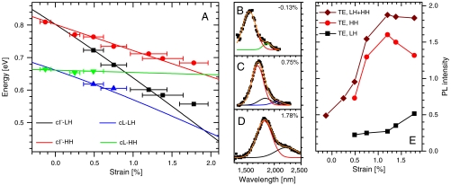
To quantify these observations, we have calculated the bandgap energies between the Γ or L conduction-band minima and the heavy-hole (HH) or light-hole (LH) valence-band maxima versus strain, using standard deformation-potential theory (2, 3, 29) with the relevant parameters chosen in accordance with available experimental data from the literature (SI Text). The results are shown by the solid lines in Fig. 4A, where the change from indirect- to direct-bandgap behavior is observed as the crossing of lines at a biaxial strain of 1.9% (in agreement with the 30-band k·p calculations of ref. 13). In general, all four transitions shown in this graph can participate in the emission process. To identify their respective contributions, the PL spectra of Fig. 3 were normalized to the spectral response of the measurement setup and then numerically fitted with multiple Gaussian peaks. As an illustration, the normalized PL spectra measured at three representative strain values are shown by the symbols in Fig. 4 B–D, together with the corresponding Gaussian fits (solid lines). The peak emission energies of all the fitting curves obtained with this procedure are shown by the symbols in Fig. 4A.
Fig. 4.
Emitted-photon energy and PL intensity versus strain. (A) Symbols, peak emission energies obtained from the PL spectra of Fig. 3, plotted as a function of strain. Lines, calculated bandgap energies between the Γ or L conduction-band minima and the HH or LH valence-band maxima. (B–D) Symbols, normalized PL spectra of the NM of Fig. 3 at a strain of -0.13% (B), 0.75 % (C), and 1.78 % (D). The corresponding Gaussian fits are indicated by the solid lines. (E) Measured TE component of the direct-bandgap PL intensity and its individual cΓ-HH and cΓ-LH contributions (where distinguishable), plotted in arbitrary units as a function of strain.
Near zero strain, the HH and LH band edges are nearly degenerate, and therefore in the numerical fits we can resolve only two peaks, the direct and indirect transitions. At high strain, indirect transitions are suppressed because of the decreasing number of electrons in the L valleys, in addition to their inherent weakness. Correspondingly, the high-strain (> 1%) spectra could also only be fitted with two peaks, due to direct conduction-to-heavy-hole (cΓ-HH) and conduction-to-light-hole (cΓ-LH) transitions. At intermediate strain values, convergence of the numerical fits could be obtained with more than two peaks, indicating the simultaneous presence of both direct and indirect transitions into both valence bands (HH and LH). With these assignments, the agreement between experimental peak emission energies and theoretical bandgap energies is quite good. Possible sources of discrepancy include small heating of the NM by the strong PL pump pulses, leading to a decrease in the bandgap energies, and band filling effects causing a blue shift in the energy of peak emission relative to the bandgap (2, 3). The numerical-fit results shown in Fig. 4A demonstrate a very large strain-induced red shift of the cΓ-LH transition, from 1,535 to 2,227 nm as the strain increases to 1.78%.
In Fig. 4E, we show the strain dependence of the measured direct-bandgap PL intensity, together with its individual cΓ-HH and cΓ-LH contributions where distinguishable, as obtained from the integrated areas under the corresponding fitting peaks. It should be noted that these PL signals are collected along the sample surface normal, and therefore only correspond to the transverse electric (TE) (i.e., in-plane polarized) emission. In contrast, most of the photons created via electron/LH recombination under biaxial strain have transverse magnetic (TM) polarization (2, 3) (i.e., linear along the axis perpendicular to the surface), and therefore propagate in the plane of the NM and cannot be detected in our geometry. This selection rule is particularly strong under high tensile strain because of the resulting increase in the fractional pz character of the LH states (z being the direction normal to the surface) (14). For example, calculations show that at the highest strain measured with this NM (1.78%), the momentum matrix element of the cΓ-LH transitions is predominantly TM polarized by a factor of over 15 in magnitude squared (see Materials and Methods). These considerations explain why the largest contribution to the measured emission is consistently provided by cΓ-HH transitions, despite the higher energy and therefore larger hole occupancy of the LH band under tensile strain. Furthermore, once the TM components of the luminescence are properly accounted for, the overall strain-induced enhancements in PL intensities are found to be much larger than suggested by Fig. 4E. Specifically, we estimate that at 1.78% strain the total cΓ-LH emission of the NM under study has increased relative to its zero-pressure value by a factor of about 20 (see Materials and Methods). In contrast, for the cΓ-HH transitions, a smaller increase by only about three is obtained, due to the lowering of the HH valence band below the LH one (and corresponding decrease in HH population) with increasing tensile strain. Eventually, this trend more than compensates for the concomitant increase in electron density at Γ, and the cΓ-HH PL intensity begins to decrease.
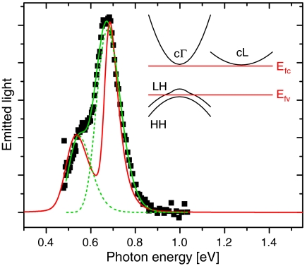
The ability to resolve clearly the cΓ-HH and cΓ-LH contributions to the PL spectra at the highest measured strain also offers a unique opportunity to estimate the quasi-equilibrium carrier density N produced by the pump pulses, and therefore ascertain whether the NM may already be pumped above transparency. To that purpose, we used standard formulas (2, 3) to calculate the TE-polarized spontaneous-emission spectrum due to both cΓ-HH and cΓ-LH transitions (see SI Text). If we assume perfectly parabolic energy bands, the required expressions only depend on a few materials parameters that can be calculated as a function of strain using data from the literature. The only fitting parameter, besides an overall multiplicative factor, is therefore N, which is selected based on the relative height of the experimental cΓ-HH and cΓ-LH emission peaks.
In Fig. 5, the symbols show the normalized PL spectrum measured at 1.78% strain, the green line is the double-Gaussian fit from Fig. 4D, and the red line is the calculated emission spectrum. The agreement with the data is quite good, except for the dip between the two peaks in the theoretical spectrum, which can be ascribed to the assumption of parabolic bands. In reality, as we move down in energy from the top of the LH band toward the top of the HH band, the LH band becomes increasingly nonparabolic (13), as illustrated in the schematic band diagram in the inset of Fig. 5; as a result, its effective mass increases, leading to increased joint density of states and therefore increased light emission. From the fit, we infer a reasonable value of N = 3.9 × 1018 cm-3, which can then be used to calculate the electron and hole quasi-Fermi levels Efc and Efv. The results are shown in the inset of Fig. 5, where the relative positions of the band edges and of the quasi-Fermi levels correspond to their calculated values. The important conclusion here is that the calculated energy separation Efc-Efv (589 meV) is larger than the cΓ-LH bandgap energy (500 meV), which is the fundamental condition for population inversion. Therefore, the same NM under the same strain and pumping conditions, placed in a suitable waveguide for in-plane radiation, would provide optical gain across the cΓ-LH bandgap. In the present experimental configuration, the propagation length of the detected light in the NM is too short (≤ 40 nm) to allow for any appreciable stimulated emission and optical amplification.
Fig. 5.
Numerical modeling of Ge NM luminescence at high strain. Symbols, normalized PL spectrum of the NM of Fig. 3 at a strain of 1.78%. Green lines, Gaussian fits showing the cΓ-HH and cΓ-LH contributions (dashed) and their sum (solid). Red line, calculated spontaneous-emission spectrum. The vertical axis is in arbitrary units. (Inset) Schematic band diagram of Ge at a strain of 1.78%, and estimated positions of the quasi-Fermi levels relative to the band edges in the presence of the PL pump pulses.
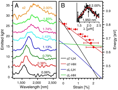
Finally, Fig. 6A shows several PL spectra measured with a thinner (24 nm) Ge NM at different strains. The emitted power levels in this case are substantially lower than in Fig. 3, attributable to smaller pump light absorption and increased nonradiative surface recombination in thinner samples. As a result, the weaker, longer-wavelength emission peaks due to cΓ-LH transitions cannot be unambiguously resolved in these luminescence spectra. At the same time, the smaller NM thickness allows reaching strain values up to 2.00% (above the threshold for turning Ge into a direct-bandgap material) with higher structural integrity across the NM area. The normalized PL spectrum measured at 2.00% strain is plotted in the inset of Fig. 6B together with a single-peak numerical fit. The emission wavelength inferred from this fit is 1,950 nm, longer than the calculated cΓ-HH bandgap wavelength at the indirect-to-direct transition point. Therefore, both strain and PL measurements here indicate the formation of direct-bandgap Ge. This conclusion is clearly illustrated in Fig. 6B, where the peak emission energies from Fig. 6A are plotted as a function of strain together with the theoretical bandgap energies. Once again, the agreement between theory and experiments is quite good.
Fig. 6.
Strain-dependent luminescence properties of a 24-nm-thick Ge NM. (A) PL spectra of a 24-nm-thick Ge NM at different levels of biaxial tensile strain (shifted vertically relative to one another for the sake of illustration clarity). The vertical axis is in arbitrary units. A small degree of smoothing (three-adjacent-points averaging) has been applied to these data. (B) Symbols, peak emission energies obtained from the PL spectra of A, plotted as a function of strain. Lines, calculated bandgap energies between the Γ or L conduction-band minima and the HH or LH valence-band maxima. (Inset) Normalized PL spectrum of the NM of A, measured at a tensile strain of 2.00% (symbols) and corresponding Gaussian fit (solid line).
Conclusion
In conclusion, we show that Ge NMs under biaxial tensile strain can enable efficient light emission and population inversion. Although in the present work the NMs are mechanically strained using high-pressure gas, we expect that similar results can be obtained on integrated silicon chips using suspended platforms loaded with suitable stressor layers or electrostatic actuators, as are commonly fabricated with MEMS technology. A possible implementation, based on a cross-shaped cantilever with all four sides attached on rigid supports (so as to allow for the introduction of biaxial strain), is proposed in the theoretical work of ref. 12.
Furthermore, electrical injection can be achieved using a lateral p-i-n junction geometry, as already demonstrated in a recent report of flexible Ge NM photodiodes (26). Therefore, tensilely strained Ge NMs represent a promising materials platform for the development of CMOS-compatible group-IV photonic devices, including electrically driven diode lasers. Additional improvements in the NM radiative properties can be expected with further optimization of the fabrication process, e.g., by reducing surface roughness, crack initiation sites, and dislocation density in the starting material to increase the strain threshold for cracking, and by using surface passivation schemes to minimize surface recombination. Suitable in-plane waveguiding elements compatible with the polarization selection rules of the cΓ-LH transitions include ridge structures and photonic crystals. Finally, it should be noted that the NM emission wavelength can be actively tuned via strain control over a wide range within the short-wave infrared spectrum. This feature is attractive for several important application areas of midinfrared optoelectronics, such as spectroscopy and biochemical sensing, that would benefit strongly from the large-scale integration of electronics and photonics (30).
Materials and Methods
Nanomembrane Fabrication.
Free-standing Ge NMs are fabricated by releasing the Ge layers of commercial (001) GOI substrates with a miscut of 6° toward [110]. The GOI wafers (Soitec SSA) are fabricated via bonding oxidized Ge to oxidized Si and etching back (SmartCut). Because the thermal-expansion coefficients of SiO2 and Ge differ, the Ge template may contain strain nonuniformities of the order of 0.1% and some dislocations. The GOI substrates are cleaned with acetone and isopropyl alcohol and patterned with UV lithography to define the membrane boundaries and small etchant access holes, which can be seen in the NM micrograph of Fig. 1A. Reactive ion etching is employed to etch the Ge template layer along these boundaries, followed by a wet etch in a mixture of 49% hydrofluoric acid and water solution (1/10) to dissolve the underlying SiO2 layer. The resulting Ge NMs settle onto and weakly bond to the original Si host wafer. The NMs are subsequently transferred and bonded onto 125-μm-thick, flexible PI films (Kapton, Du Pont) by using spin-on liquid PI as a glue layer and pressing the membrane onto the PI film. After transfer, the spin-on PI is cured at 350 °C and the Ge NM is thinned from its original thickness (84 ± 2 nm) to the desired thickness using a wet etch with dilute hydrogen peroxide (H2O2) in water at 80 °C (etch rate ca.0.9 nm/s).
Raman Measurements.
The strain in the plane of the NMs is determined as a function of applied stress (i.e., gas pressure) via Raman spectroscopy, using a LabRAM ARAMIS (HORIBA Scientific) Raman microscope equipped with a 633-nm-wavelength excitation laser. In these measurements, the laser beam is passed through a filter to attenuate its incident power from 6 mW to approximately 1 mW and then focused onto the NM with a 50× objective lens, producing a spot size of about 2 μm. Because of the low thermal conductivity of the PI film supporting the NM, the use of sufficiently low incident power is required to avoid heating the NM, which would affect the Raman shifts and therefore the inferred strain values. Ten random sites on each NM are measured for each value of the applied stress, and each site is probed three times with a 15-s exposure time. The peak position of the Raman signal is determined from a Gauss–Lorentz fit of the measured spectra after background subtraction, and the biaxial strain values are then calculated from the Raman shifts (16) using the previously measured phonon deformation potentials for Ge (31).
Photoluminescence Measurements.
The light-emission properties of the NMs are investigated via room-temperature PL studies. The pump light is provided by a tunable optical parametric oscillator and consists of a train of pulses having 5-ns width, 20-Hz repetition rate, 960-nm wavelength, and 3-mW average power (0.15-mJ pulse energy) focused onto the NM with a spot size of about 1 mm. The emitted light is dispersed through a monochromator and finally measured using a room-temperature extended-range InGaAs photodetector with 1.2- to 2.6-μm spectral response and 45-MHz bandwidth. To increase the measurement sensitivity, gated detection is performed using a boxcar integrator. The measured PL spectra are normalized to the spectral response of the setup, which is determined by the reflectivity of the monochromator grating and the responsivity of the photodiode.
Simulations.
The bandgap energies between the Γ or L conduction-band minima and the HH or LH valence-band maxima are computed as a function of strain using standard deformation-potential theory (2, 3, 29). The key parameters of this theory were chosen based on available experimental data from the literature, as discussed in the SI Text. The TE-polarized cΓ-HH and cΓ-LH spontaneous-emission spectra are calculated using textbook formulas (2, 3) involving the joint densities of states, Fermi distribution functions, and oscillator strengths, based on the assumptions of perfectly parabolic energy bands. To account for the experimentally observed strain variations across the NM area at fixed pressure, these theoretical spectra are convoluted with a Gaussian function of strain, with mean value and standard deviation based on the Raman measurement results. More details about these calculations are presented in the SI Text.
PL Intensity Data Analysis.
The overall strain-induced enhancements in light-emission efficiency are obtained from the experimental data by first estimating the TE and TM components of both cΓ-HH and cΓ-LH luminescence, at zero pressure and at the highest measured strain. Near zero strain, the cΓ-HH and cΓ-LH contributions to the measured TE emission are degenerate and therefore only their sum can be experimentally determined. Their individual intensities are then computed based on the ratio of their respective reduced effective masses (2, 3). Furthermore, near zero strain the emission is isotropic and therefore has equal TE and TM components because of the cubic symmetry of the Ge crystal structure. At the highest strain (1.78% in Figs. 3 and 4), the TE components of the cΓ-HH and cΓ-LH PL intensities are obtained independently from the measured spectra, as shown in Fig. 4E. The corresponding TM components are then estimated from the calculated ratios of the TE and TM components of the momentum matrix elements squared. The latter parameters are calculated from the Bloch functions of electrons, HHs, and LHs as described in refs. 2 and 3; the strain dependence of the Bloch functions is also included in this computation, following ref. 32. The emission enhancements are then obtained by comparing the total cΓ-HH or cΓ-LH PL intensities (each given by twice the TE component plus the TM component) at zero pressure and 1.78% strain.
Supplementary Material
Acknowledgments.
This work was primarily supported by the National Science Foundation under Grant DMR-0907296. Nanomembrane fabrication, straining, and Raman measurements were supported by Department of Energy Grant DE-FG02-03ER46028 (to J.R.S.-P., F.C., and R.J.). D.M.P. acknowledges support from the National Science Foundation and National Defense Science and Engineering Graduate Research Fellowship Programs.
Footnotes
The authors declare no conflict of interest.
This article is a PNAS Direct Submission.
This article contains supporting information online at www.pnas.org/lookup/suppl/doi:10.1073/pnas.1107968108/-/DCSupplemental.
References
- 1.Chu M, Sun YK, Aghoram U, Thompson SE. Strain: A solution for higher carrier mobility in nanoscale MOSFETs. Annu Rev Mater Res. 2009;39:203–229. [Google Scholar]
- 2.Chuang SL. Physics of Photonic Devices. Hoboken, NJ: Wiley; 2009. chaps. 4, 9, and 10. [Google Scholar]
- 3.Coldren LA, Corzine SW. Diode Lasers and Photonic Integrated Circuits. New York: Wiley; 1995. chap. 4, appendices 10 and 11. [Google Scholar]
- 4.Matthews JW, Blakeslee AE. Defects in epitaxial multilayers: 1. Misfit dislocations. J Cryst Growth. 1974;27:118–125. [Google Scholar]
- 5.Roberts MM, et al. Elastically relaxed free-standing strained-silicon nano-membranes. Nat Mater. 2006;5:388–393. doi: 10.1038/nmat1606. [DOI] [PubMed] [Google Scholar]
- 6.Scott SA, Lagally MG. Elastically strain-sharing nanomembranes: Flexible and transferable strained silicon and silicon-germanium alloys. J Phys D Appl Phys. 2007;40:R75–R92. [Google Scholar]
- 7.Euaruksakul C, et al. Influence of strain on the conduction band structure of strained silicon nanomembranes. Phys Rev Lett. 2008;101:147403. doi: 10.1103/PhysRevLett.101.147403. [DOI] [PubMed] [Google Scholar]
- 8.Huang MH, et al. Mechano-electronic superlattices in silicon nanoribbons. ACS Nano. 2009;3:721–727. doi: 10.1021/nn8008883. [DOI] [PubMed] [Google Scholar]
- 9.Fischetti MV, Laux SE. Band structure, deformation potentials, and carrier mobility in strained Si, Ge, and SiGe alloys. J Appl Phys. 1996;80:2234–2252. [Google Scholar]
- 10.Menéndez J, Kouvetakis J. Type-I Ge/Ge1-x-ySixSny strained-layer heterostructures with a direct Ge bandgap. Appl Phys Lett. 2004;85:1175–1177. [Google Scholar]
- 11.Liu J, et al. Tensile-strained, n-type Ge as a gain medium for monolithic laser integration on Si. Opt Express. 2007;15:11272–11277. doi: 10.1364/oe.15.011272. [DOI] [PubMed] [Google Scholar]
- 12.Lim PH, Park S, Ishikawa Y, Wada K. Enhanced direct bandgap emission in germanium by micromechanical strain engineering. Opt Express. 2009;17:16358–16365. doi: 10.1364/oe.17.016358. [DOI] [PubMed] [Google Scholar]
- 13.El Kurdi M, Fishman G, Sauvage S, Boucaud P. Band structure and optical gain of tensile-strained germanium based on a 30 band k·p formalism. J Appl Phys. 2010;107:013710. [Google Scholar]
- 14.Pizzi G, Virgilio M, Grosso G. Tight-binding calculation of optical gain in tensile strained [001]-Ge/SiGe quantum wells. Nanotechnology. 2010;21:055202. doi: 10.1088/0957-4484/21/5/055202. [DOI] [PubMed] [Google Scholar]
- 15.Huo Y, et al. Strong enhancement of direct transition photoluminescence with highly tensile-strained Ge grown by molecular beam epitaxy. Appl Phys Lett. 2011;98:011111. [Google Scholar]
- 16.Fang YY, et al. Perfectly tetragonal, tensile-strained Ge on Ge1-ySny buffered Si(100) Appl Phys Lett. 2007;90:061915. [Google Scholar]
- 17.Liu J, Sun X, Camacho-Aguilera R, Kimerling LC, Michel J. Ge-on-Si laser operating at room temperature. Opt Lett. 2010;35:679–681. doi: 10.1364/OL.35.000679. [DOI] [PubMed] [Google Scholar]
- 18.Jayaraman A. Diamond anvil cell and high-pressure physical investigations. Rev Mod Phys. 1983;55:65–108. [Google Scholar]
- 19.Freund LB, Suresh S. Thin Film Materials: Stress, Defect Formation and Surface Evolution. Cambridge, UK: Cambridge Univ Press; 2003. [Google Scholar]
- 20.El Kurdi M, et al. Control of direct band gap emission of bulk germanium by mechanical tensile strain. Appl Phys Lett. 2010;96:041909. [Google Scholar]
- 21.Cheng TH, et al. Strain-enhanced photoluminescence from Ge direct transition. Appl Phys Lett. 2010;96:211108. [Google Scholar]
- 22.Rogers JA, Lagally MG, Nuzzo RG. Synthesis, assembly, and applications of semiconductor nanomembranes. Nature. 2011;477:45–53. doi: 10.1038/nature10381. [DOI] [PubMed] [Google Scholar]
- 23.Yoon J, et al. Ultrathin silicon solar microcells for semitransparent, mechanically flexible and microconcentrator module designs. Nat Mater. 2008;7:907–915. doi: 10.1038/nmat2287. [DOI] [PubMed] [Google Scholar]
- 24.Ko HC, et al. A hemispherical electronic eye camera based on compressible silicon optoelectronics. Nature. 2008;454:748–753. doi: 10.1038/nature07113. [DOI] [PubMed] [Google Scholar]
- 25.Kim DH, et al. Stretchable and foldable silicon integrated circuits. Science. 2008;320:507–511. doi: 10.1126/science.1154367. [DOI] [PubMed] [Google Scholar]
- 26.Yuan HC, et al. Flexible photodetectors on plastic substrates by use of printing transferred single-crystal germanium membranes. Appl Phys Lett. 2009;94:013102. [Google Scholar]
- 27.Thurmer DJ, Bof Bufon CC, Deneke C, Schmidt OG. Nanomembrane-based mesoscopic superconducting hybrid junctions. Nano Lett. 2010;10:3704–3709. doi: 10.1021/nl1022145. [DOI] [PubMed] [Google Scholar]
- 28.Feng P, et al. Local-illuminated ultrathin silicon nanomembranes with photovoltaic effect and negative transconductance. Adv Mater. 2010;22:3667–3671. doi: 10.1002/adma.201000583. [DOI] [PubMed] [Google Scholar]
- 29.Van de Walle CG. Band lineups and deformation potentials in the model-solid theory. Phys Rev B Condens Matter Mater Phys. 1989;39:1871–1883. doi: 10.1103/physrevb.39.1871. [DOI] [PubMed] [Google Scholar]
- 30.Soref R. Mid-infrared photonics in silicon and germanium. Nat Photonics. 2010;4:495–497. [Google Scholar]
- 31.Cerdeira F, Buchenauer CJ, Cardona M, Pollak FH. Stress-induced shifts of first-order Raman frequencies of diamond- and zinc-blende-type semiconductors. Phys Rev B Condens Matter Mater Phys. 1972;5:580–593. [Google Scholar]
- 32.Jones G, O’Reilly EP. Improved performance of long-wavelength strained bulk-like semiconductor lasers. IEEE J Quantum Electron. 1993;29:1344–1354. [Google Scholar]
Associated Data
This section collects any data citations, data availability statements, or supplementary materials included in this article.


