

Abstract
We present an active full-wave rectifier with offset-controlled high speed comparators in standard CMOS that provides high power conversion efficiency (PCE) in high frequency (HF) range for inductively powered devices. This rectifier provides much lower dropout voltage and far better PCE compared to the passive on-chip or off-chip rectifiers. The built-in offset-control functions in the comparators compensate for both turn-on and turn-off delays in the main rectifying switches, thus maximizing the forward current delivered to the load and minimizing the back current to improve the PCE. We have fabricated this active rectifier in a 0.5-μm 3M2P standard CMOS process, occupying 0.18 mm2 of chip area. With 3.8 V peak ac input at 13.56 MHz, the rectifier provides 3.12 V dc output to a 500 Ω load, resulting in the PCE of 80.2%, which is the highest measured at this frequency. In addition, overvoltage protection (OVP) as safety measure and built-in back telemetry capabilities have been incorporated in our design using detuning and load shift keying (LSK) techniques, respectively, and tested.
Index Terms: Active rectifier, back telemetry, high speed comparators, implantable microelectronic devices, inductive power transmission, load shift keying, offset control, RFID
I. Introduction
Implantable microelectronic devices (IMD) powered by internal batteries suffer from their large volume, limited lifetime, replacement hardship, and cost. Therefore, they are only suitable for medical treatments with ultra low power requirements, such as pacing the heart, which have extended battery lifetimes in the range of several years [1]. On the other hand, there are treatments, such as neuroprostheses like cochlear and retinal implants, which require orders of magnitude higher currents for stimulation or recording regardless of the circuit efficiency [2]. There are also applications such as radio frequency identification (RFID), in which the size and cost of neither primary nor secondary (i.e., rechargeable) batteries are justified [3]. To address these limitations, wireless power transmission techniques using inductive links have been utilized to supply size-, cost-, and power-constrained devices and applications.
Inductively powered systems in general consist of three main components: reader, inductive link, and transponder, as shown in Fig. 1. On the reader side, which is also the power transmitter, a power amplifier drives the primary coil, L1, at the power carrier frequency, fc. This signal is induced on to the secondary coil, L2, through the inductive link, and generates an ac voltage across the transponder resonance circuit, L2 and C2. Following the L2C2 tank, there is always a rectifier to convert the ac signal to dc (VREC) for supplying the rest of the transponder. The efficiency and performance of this rectifier, which is the focus of this article, is key to the overall power efficiency of the system, because all the usable received power passes through it. Since the dc voltage varies significantly with the coils’ relative distance, d, and alignment, a low dropout regulator often follows the rectifier for providing a constant supply voltage, VDD, to the IMD or RFID load.
Fig. 1.

Block diagram of an inductively powered implantable microelectronic device (IMD) with emphasis on the power transmission/conditioning circuitry.
Considering the power flow from the external energy source (i.e., the battery) to the load, RLR, the total power conversion efficiency (PCE) can be calculated from
| (1) |
where ηPA, ηlink, ηrectifier, and ηregulator are the efficiencies of the power amplifier, inductive link, rectifier, and regulator, respectively. Achieving higher PCE (ηtotal) is very important in inductively powered applications because it allows IMDs to operate with smaller received power from a larger distance. Lower received power also reduces the risk of tissue damage from overheating [2]. In the IMD applications, ηlink is limited due to the size constraint of the secondary coil [4]. The regulator, on the other hand, already has a high ηregulator because of its low dropout topology. Therefore, improving the rectifier PCE (ηrectifier) is a key factor for safe IMD operation.
Passive rectifiers using diodes or diode-connected transistors have been used in the past for inductively powered applications [5]–[9]. However, PN junction diodes induce large forward voltage drops and power dissipation. Schottky diodes have low dropout voltages [10]. However, they have a high leakage current, they are not available in most standard CMOS processes, and may need extra fabrication steps. Their reverse breakdown voltages may not be high enough either. Several VTh cancellation techniques have been proposed to reduce the passive diode voltage drop [11]–[14]. However, these are sensitive to process variations and still unable to provide high PCE. Therefore, active synchronous rectifiers using comparator controlled rectifying switches are currently considered the most promising solutions for increasing the PCE in ASICs [15]–[24]. In these rectifiers, voltage drop across the main rectifying switches is much lower than the diode voltage drop, dissipating less power within the rectifier. We previously reported power efficient active rectifiers using phase lead in [16] and [24]. The maximum operating frequency of those rectifiers, however, was limited to 1–2 MHz. Active rectifiers need significantly faster comparators to drive their switches at the right times for higher carrier frequencies, such as 13.56 MHz in the Industrial, Scientific, and Medical (ISM) band, and maximize the forward current flow, while minimizing the reverse currents.
In this paper, we propose an integrated power efficient active rectifier with offset-controlled high speed comparators for inductively powered applications. Comparators are equipped with offset control functions to compensate for both turn-on and turn-off delays, optimizing the power transfer from the secondary coil to the load (regulator). Section II presents the operating principles and the PCE analysis of our new active rectifier architecture. Section III describes the concept, implementation, and effects of the proposed offset-control functions on the high speed comparators. The simulation and measurement results are depicted in Section IV, followed by conclusions in Section V.
II. Active Rectifier Architecture
A. Operating Principle and Implementation
The new full-wave active rectifier employs a pair of high-speed comparators (CMP1 and CMP2) to drive the main rectifying elements (P1 and P2) in Fig. 2. Ideally, the input voltage of the rectifier, VIN = VIN1 − VIN2, has a sinusoidal waveform. Hence, P1 and P2 turn on alternatively depending on the polarity and amplitude of VIN.
Fig. 2.

Schematic diagram of our active rectifier including offset-controlled high speed comparators, dynamic body biasing, and load shift keying (LSK) back telemetry functions.
When VIN > VThN (the NMOS threshold voltage) and |VIN| < VREC, the positive feedback operation of the cross-coupled NMOS pair (N1 and N2) connects VIN2 to VSS through N2 and turns off N1. In this case, CMP2 output goes high because VREC > VSS, and P2 is turned off. P1 also remains off as long as |VIN| < VREC. When |VIN| > VREC, CMP1 output goes low and turns P1 on. Therefore, current flows from VIN1 to VREC, and charges the rectifier’s resistive/capacitive load (RLCL). In the next half cycle, when VIN < –VThN, VIN1 is connected to VSS through N1, N2 turns off, and both P1 and P2 are also initially off for the period of |VIN| < VREC. Then, after |VIN| > VREC, CMP2 turns P2 on and current flows from V1N2 to VREC to charge the resistive/capacitive load again.
To avoid latch-up and substrate leakage problems among P1 and P2, potentials at their separated N-well body terminals (VB1 and VB2) need to be the highest potentials on-chip. We adopted the dynamic body bias control technique from [6] and [25] by utilizing auxiliary PMOS transistors, P3 to P6. With this method, VB1 and VB2 are automatically connected to the highest potential between the input voltages, VIn1 and VIN2, and the output voltage, VREC, of the rectifier.
B. Back Telemetry and Overvoltage Protection
To add back telemetry capability, which is desired to inform the reader about the status of the IMD, deliver measured biosignals, or close the power control loop [26], [27], we have employed the load shift keying (LSK) scheme by shorting the secondary coil, L2, with the short-coil (SC) data signal [9]. A pair of NMOS switches, N3 and N4, has been added in parallel to the cross-coupled N1 and N2, respectively. When the data signal is high, the input nodes of the rectifier are shorted together, leading to increased secondary quality factor, Q2, and increased voltage across the primary coil, L1. Back telemetry data from the transponder to the reader is detected by sensing these variations across the external LSK sensing block in Fig. 1.
VIN highly depends on the coils mutual coupling, M, which is in turn highly dependent on the coils separation, d, and alignment [4]. Loading variations also change Q2 and affect VIN even when M is constant. Unexpected variations in M and RLR may cause VREC to exceed the safe voltage limits of the application or fabrication process and result in transistor breakdown. To prevent this problem, we have added an overvoltage protection (OVP) circuit to the rectifier by comparing a quarter of VREC with a constant reference voltage. When VIN exceeds a certain level, the comparator output goes high and a detuning capacitor (Covp) is added in parallel across the secondary tank circuit, as shown in Fig. 1, to reduce VIN by detuning it. The advantage of this method over current leakage based techniques [10] is that no extra heat is dissipated within the ASIC and IMD as a result of this protective safety measure.
C. PCE Analysis and Considerations
PCE depends on the size of the rectifying PMOS and the cross-coupled NMOS pairs because these transistors are in the main current path. For example, when VIN1 – VIN2 > VREC, P1 and N2 turn on and open a current path to the load, as shown in Fig. 3. In this case, the total lost power, PLoss;total, will be dominated by the switching loss of P1(PLoss,Cgp), Ron loss of P1 (PLoss,Ronp), and Ron loss of N2 (PLoss.Ronn). Since the gate of N2 is always connected to the input node of the rectifier, there is negligible switching loss for charging and discharging the gate capacitance of N2. Therefore, PLoss,total can be approximated by
Fig. 3.

Simplified schematic diagram of the active rectifier depicting the current path and power dissipating components when VIN1 – VIN2 > VREC.
| (2) |
where is the gate capacitance per unit width of P1, fc is the carrier frequency (13.56 MHz), Deff is the effective duty cycle including comparator delay, and Wp is the width of P1.
In this design, we have assumed Wn = Wp for the sake of simplicity. However, we have also proven in [24] that the optimal size ratio of the PMOS and NMOS transistors can be found from
| (3) |
where Kp =μpCox and Kn = μnCox are the PMOS and NMOS transconductances, respectively. One should note that even though larger transistor size decreases the Ron loss, it increases the switching loss and comparator delays due to the larger gate capacitance. Therefore, the main rectifying transistors have an optimal size for minimum power dissipation depending on fc and RL, which should also comply with the total chip area that is allocated to the rectifier [24].
TPHL and TPLH, the turn-on and turn-off delays of CMP1,2, affect the rectifier PCE because these delays hinder P1,2 switches from turning on and off at proper times and cause back current. Our model considers the size of the rectifying transistors and comparator delays to estimate the maximum PCE. In the Appendix, we have defined Wp, Ronp + Ronn, and Deff as functions of the switching duty cycle (D), TPHL, and TPLH, and differentiated (2) with respect to D to minimize PLoss,total. With the power loss from (2), we can estimate the maximum PCE of the rectifier
| (4) |
where PLoad is the output power, and Pcomparator is the total power consumption of each comparator excluding the charging and discharging power consumption of P1,2 gates, which has already been considered in PLoss.total.
Fig. 4 shows the calculated rectifier PCE versus Wp for various comparator delays, using parameters from the ON Semi 0.5-μum standard CMOS process. In this calculation, we assume that PLoad = 20 mW, VREC = 3.2 V, RL = 500 Ω, and Pcomparator = 0.1 mW, which are based on the simulation results. It can be seen that with Wp = 2100 μm and TPHL = TPLH = 0 ns, the rectifier achieves the highest PCE of 92%. This is the theoretical upper limit for the PCE that can be obtained by choosing optimized transistor width and eliminating the effect of comparators’ delay by utilizing offset-controlled high speed comparators that are described in Section III.
Fig. 4.

Calculated rectifier power conversion efficiency (PCE) versus Wp depending on the comparator delays when VREC = 3.2 V and RL = 500 Ω. Curve-a: TPHL = 0 ns and TPLH = 0 ns; Curve-b: TPHL = 5 ns and TPLH = 0 ns; Curve-c: TPHL = 0 ns and TPLH = 3 ns; Curve-d: TPHL = 3 ns and TPLH = 3 ns; Curve-e: TPHL = 0 ns and TPLH = 4 ns; and Curve-f: TPHL = 4 ns and TPLH = 4 ns.
III. Offset-Controlled High Speed Comparators
A. Concept of the Offset-Control Function
In order to drive the large rectifying PMOS transistors at high operating frequency of 13.56 MHz, high speed comparators with low power consumption and high driving capability are required. Typically, the comparator operating speed is limited by its propagation delay, TP, which is how quickly the output responds to a change at the input. In this rectifier application, the comparator propagation delay adversely affects the PCE. Due to TPHL, the comparators turn P1,2 on too late and reduce the input power that could otherwise be transferred to the load during this delay. Moreover, due to TPLH, comparators lag in turning P1,2 off, and current can instantaneously flow from CL back to the secondary coil when VIN < VREC.
Since it is not possible to reduce TP to zero, in order to overcome such limitations, we have utilized offset control function in the high speed comparators used in this rectifier. Fig. 5 shows the block diagram of this comparator, which consists of a common-gate type comparator (CG Cmp), two offset-control blocks (OffsetF and OffsetR), and current-starved (CS) inverters. Offset-control blocks inject a programmable offset current, OSF and OSR, to the inputs of the CG comparator alternately depending on the state of the VOUT feedback signals, FBF and FBR. Therefore, VOUT expedites the falling or rising transition by sensing them ahead of time.
Fig. 5.

Block diagram of the high speed comparator employing offset control functions for both falling and rising VOUT transitions.
Segment-(a) in Fig. 6 exhibits a falling VOUT transition, occurring when |VIN| = |VIN1 – VIN2| > VREC. At this point, the CG comparator output, VOUT, falls to turn on P1 (or P2). FBF is low during this period, and only the OffsetF block operates to inject offset current to the negative input of the CG comparator. With the help of OffsetF, VOUT can be forced to fall even before |VIN| exceeds VREC at the end of segment-a, compensating for the comparators’ turn-on delay. It is important, however, to note that OffsetF has to be turned off after the VOUT falling transition so that it does not affect the following VOUT rising transition. Otherwise, OffsetF can delay the rising VOUT transition, which is counterproductive. This is why in Fig. 5 the OffsetF block receives a feedback signal from VOUT and properly turns off after every falling transition of VOUT.
Fig. 6.

Simulated waveforms and timing diagram showing the operation of the offset-control blocks in the high speed comparators.
On the other hand, during the VOUT rising transition in segment-(b), when |VIN| < VREC, FBR that has gone low after VOUT falling, turns on the OffsetR block. The OffsetR block injects offset current to the positive input of the CG comparator and can force VOUT to start rising even before |VIN| falls below VREC. This helps P1 (or P2) to turn off at a proper time and prevents the back current.
If the OffsetR block turns on just after VOUT starts to fall, this instantaneous negative feedback mechanism hinders VOUT from falling down fully and causes VOUT to fluctuate. To avoid this problem, we have added two current-starved inverters in the feedback loop to add a delay between VOUT, FBF, and FBR transitions, thus assuring stable comparator feedback operation. This delay does not need to be precise as long as it is less than one carrier cycle period. It results in a short period, segment-(c), during which both OffsetF and OffsetR blocks are on.
B. Circuit Implementation
Fig. 7 shows the schematic diagram of the high speed comparator with two offset-control functions, OffsetF and OffsetR. Without considering offset-control blocks and CS inverters, it basically works as a simple common-gate comparator with start-up capability [15]. Two input voltages, VREC and VIN1, are applied to the sources of input transistors, P7 and P8, respectively. When VIN1 > VREC, the current flowing through P8 becomes larger than that of P7. Therefore, the gate voltage of the output inverter, VA, rapidly increases, and VOUT falls to turn P1 on. The OffsetF and OffsetR blocks are implemented by using current sources, P13–P14 and P10–P11, within the comparator, MUXs, and the control switches, P15 and P12. These blocks inject offset currents to the comparator inputs alternatively, inducing the desired timing. For example, when VOUT is high, P15 turns on, and an offset current flows into the comparator positive input branch (VREC) through OSF, causing VA to increase. Therefore, VOUT starts to fall earlier before VIN1 exceeds VREC. The offset current is programmable by using 2-bit off-chip control signals per offset-control block, CTL0:1 and CTL2:3, in order to adjust the rectifier timing in response to process variations.
Fig. 7.

Schematic diagram of the high speed comparator with two offset-control functions, OffsetF for the VOUT falling edge and OffsetR for the VOUT rising edge.
C. Effects of Offset-Control Functions on PCE
Simulation results depicting the relationship between the PCE and offset-control functions are shown in Fig. 8. To understand the effects of the offset-control functions better, we have overlapped the rectifier input/output voltages, input current, and input power waveforms while adjusting VIN amplitude to achieve a constant VOUT = 3.2 V for RL = 500 Ω. Fig. 8(a) shows that with no comparator offset-control function in place, the back current resulting from the turn-off delay severely degrades the PCE. This back current can be prevented by using the OffsetR function, as shown in Fig. 8(b). Even though OffsetR improves the PCE significantly, the input power to the rectifier is still being reduced due to the comparators’ turn-on delay, TPHL. Therefore, there is room to further improve the rectifier PCE as well as voltage conversion efficiency (VCE) by using both OffsetF and OffsetR functions to compensate for TPHL and TPLH delays, respectively. Fig. 8(c) clearly shows that with both functions in place VOUT transitions happen at the right times, and the PCE is maximized.
Fig. 8.

Simulation results of the active rectifier showing waveforms of the input/output voltages, input current, and input power with VREC = 3.2 V and RL = 500 Ω, (a) without any offset-control function, (b) with only OffsetR function, and (c) with both OffsetF and OffsetR functions.
Since the offset-control blocks consume additional power to provide the offset currents, the power overhead for employing these functions needs to be considered. Fig. 9 shows the simulated comparator power consumption versus VREC and its break down between the two blocks. When VREC increases, the power consumption of the CG comparator, curve-(b) also increases, contributing a large portion of the comparator power consumption, curve-(a). This is because both the static current of the CG comparator and the shoot-through current of the output inverter increase with VREC. Moreover, since the comparator offsets have been tuned for VREC = 3.12 V, power consumption becomes more severe at higher VREC. On the other hand, curve-(c), the offset-control blocks’ power consumption shows a mild increase when VREC increases. It is because the offset-control blocks consume only dynamic power for a short period. For VREC = 3.12 V, the entire high speed comparator consumes 135 μW, 40 μW of which is the power consumption of the offset-control blocks. The entire comparator power consumption is little affected by the load conditions as long as VREC is fixed.
Fig. 9.

Simulated power consumption of the comparator versus VREC showing power overheads for employing the offset-control functions (fc = 13.56 MHz, RL = 500 Ω, and CL = 10 μF). Curve (a) shows the total power consumption of the high speed comparator, (b) is the power consumption of the CG comparator and CS inverters, and (c) indicates the consumption of the offset-control blocks.
D. Startup Capability
Since no supply voltage is available before the active rectifier starts its operation, it is necessary for the rectifier to have self startup capability. Our high speed comparator, shown in Fig. 7, has a common-gate input stage, in which the two comparator input voltages, VIN1 and VREC, are also the positive supply voltages. Hence the rectifier sinusoidal input voltage, VIN1,2, guarantees that the rectifier reliably starts up even before VREC is sufficiently charged up. For example, when VREC = 0 V, the input voltage of the output inverter, VA, follows VIN1 through P8, since N6 is turned off. Therefore, when VIN1 > VThN7, VOUT of the comparator will be connected to VSS through N7 leading the rectifying PMOS to turn on and charge VREC.
Since the comparator bias current is generated by P7–P9–N5 branch, it properly turns on when VREC > VThP7 + VThN5. On the other hand, when 0 < VREC < VThP7 + VTHN5, the comparator still turns on the rectifying PMOS for conducting current to VREC, as explained above, but it does not turn them off at the right time, resulting in back current. Now, if VIN,peak is high enough (> 2.9 V in our design), then it will be sufficient for charging VREC to surpass the VTHP7 + VTHN5 level even in the presence of the back current. While VREC is being charged, the gate voltage of N5,6 also increases, and VA decreases to turn off the rectifying PMOS during VIN1 < VREC. Moreover, the comparator operation and the rectifier PCE move towards their optimal points as VREC increases toward the target value of 3.12 V. Therefore, once VREC exceeds VThP7 + VThN5, it can easily charge up to 3.12 V. Fig. 10 shows simulated waveforms for the rectifier self startup process, which guarantees that VREC is charged up to 3.12 V when VIN,peak = 3.4 V (3.8 V in measurements). In this design, for an input voltage of VIN,peak = 2.9 V (3.2 V in meas.), the suboptimal operation of the rectifier results in VREC = 2.5 V.
Fig. 10.

Simulated waveforms for self startup operation of the active rectifier (fc = 13.56 MHz, VIN,Peak = 3.4 V, VREC = 3.12 V, RL = 500 Ω, and CL = 2.5 nF).
IV. Simulation and Measurement Results
The active rectifier was fabricated in the ON Semiconductor 0.5-μm 3M2P standard CMOS process (minimum transistor length of 0.6 μm) for its relatively high voltage handling capability. Fig. 11 shows the chip micrograph, which includes the active rectifier, overvoltage protection circuit, and the low dropout regulator, occupying 0.4 mm2 of the Si area with Wp/Lp = Wn/Ln = 2100 μm/0.6 μm. Since each comparator offset-control function can be enabled or disabled by external control lines, we were able to evaluate the rectifier performance with and without the comparator offset functions.
Fig. 11.

Fabricated chip micrograph and its floor plan, including the active rectifier, overvoltage protection circuit, and low dropout regulator.
A. Measured Waveforms and Parasitic Effects
Fig. 12 shows the lumped model of the circuit used in the rectifier measurements with emphasis on the inductive and capacitive parasitic components, which combined with the measurement instrument (oscilloscope) parasitic, cause distortion in the measured waveforms at this relatively high operating frequency (fc = 13.56 MHz). For instance, when the rectifier starts conducting, there is a sudden drop in VIN1 – VIN2, and when it stops conducting, the stored energy in the interconnect inductors cause a sudden voltage hike across the rectifier inputs. Therefore, it is important to note that the voltages measured across the coil or load, VXY, are not exactly the same as those measured on the rectifier packaged IC pins, (LQFP176). For example, Lbond, the parasitic inductance of the wirebond, and Lwire, the parasitic inductance of the external interconnects, cause the rectifier input voltage at the package, , to be distorted and have a peak voltage higher than the sinusoidal input voltages at the secondary coil, VIN1 – VIN2.
Fig. 12.

Lumped model of the circuit used in active rectifier simulations, showing capacitive and inductive parasitic components of the wire-bond and external interconnects. It is important to note that because of these parasitics, voltages measured on the coil or load, VXy, are not exactly the same as those measured on the asic package (lqfp176), VXy*.
Moreover, the instantaneous input current flows into the rectifier through the parasitic inductors only during the rectifier turn-on, which is much shorter than one operating cycle (see Fig. 8(c). Therefore, the frequency components, which affect the parasitic inductors and distort the voltage waveforms, are effectively much higher than the carrier frequency at 13.56 MHz. Unfortunately, this effect has not been considered in the recent literature on active rectifiers, and consequently, depending on how the measurements are done, the reported results on the rectifier efficiency might have been optimistic.
Fig. 13 shows the active rectifier measured input and output voltage waveforms. In these measurements we refrained from directly probing VOUT because it could load and affect the comparator performance. Instead, CL was reduced from 10 μF to 100 pF to better show the effects of offset-control functions. For all measurements and simulations in this section, we enabled the OffsetR to prevent the back currents. When the OffsetF function was enabled, VREC started to increase ~ 5 ns earlier than without OffsetF. This comparison, which is consistent with the simulation results in Fig. 8, shows that the comparators turn the rectifier on faster to deliver current for a longer time period. Therefore, the OffsetF function not only improves the PCE but also reduces the rectifier dropout voltage, Vdrop, which is defined as the difference between VIN1,Peak* and VREC. There is also a small phase shift between the ripple on VREC and VIN1,2* due to the parasitic components.
Fig. 13.

Measured waveforms of the input and output voltages of the rectifier with and without the OffsetF function (fc = 13.56 MHz, VIN,peak = 4.1 V, RL = 500 Ω, and CL = 100 pF).
B. PCE and Dropout Voltage Measurements
We measured the PCE and Vdrop by sweeping 1) VREC ;2) RL connected directly across the rectifier, substituting the regulator; and 3) fc. In order to measure the rectifier input current, we connected a small resistor, Rsense = 10 Ω, in series with the rectifier input as a current sensor and differentially measured the voltage across it. The rectifier input power was calculated offline by integrating the instantaneous product of the input current and voltage samples. The output power for the PCE was obtained by measuring the VREC,RMS. The peak input voltage, VIN,Peak, can be expressed as the sum of VREC and Vdrop.
Fig. 14 shows the measured and simulated PCE and Vdrop versus VREC with CL = 10 μF, RL = 500 Ω, and fc = 13.56 MHz. All simulated results in this section are postlayout and include the estimated parasitic components of the LQFP176 package (see Fig. 12). Fig. 14(a) shows that for VREC = 3.12 V, the maximum PCE with both offset-control functions was measured to be 80.2% (curve-b), which was slightly lower than the maximum postlayout simulated PCE of 84.5% (curve-a) and schematic simulated PCE of 87% due to the effects of parasitics and the current sensing resistor. The measured PCE without OffsetF (curve-c) is ~ 10% lower than the PCE with Offset F. When VREC was higher or lower than 3.12 V, the PCE gradually decreased because the comparator offsets were only adjusted for VREC = 3.1–3.2 V. For other VREC values, the comparator offsets can be easily readjusted using CTL0:3 in Fig. 2.
Fig. 14.

Measured and simulated (a) PCE and (b) Vdrop versus VREC when RL = 500 Ω, CL = 10 μF, and fc = 13.56 MHz.
In Fig. 14(b), the measured Vdrop with OffsetF (curve-b) shows 0.7 V dropout, which is 0.4 V higher than the simulated Vdrop with OffsetF (curve-a). This is due to the interconnect inductances increasing as explained earlier. For example, was measured ~ 250 mV higher than VIN1,Peak in Fig. 12 after shorting Rsense. By including these parasitic inductors in our simulations (Lbond + Lwire = 25 nH), we were able to verify the cause of Vdrop variations by producing results (curve-d) that were closer to the measured Vdrop (curve-b). Vdrop is also affected by the output current, IREC, and PCE. In Fig. 14(b), a higher VREC with fixed RL requires higher IREC through the rectifier, which generates a larger voltage drop across the rectifying transistors, increasing Vdrop. Furthermore, a rectifier with lower PCE requires more current from the coil to reach a certain VREC, which also increases Vdrop. Overall, measured and simulated results clearly showed that Vdrop is reduced by using both offset-control functions.
Fig. 15(a) shows the measured and simulated PCE versus RL with CL = 10 μF, VREC = 3.12 V, and fc = 13.56 MHz. As RL increases, the rectifier output power for the same VREC decreases. Therefore, the rectifier internal power dissipation for switch losses, PLoss,total, and comparators, Pcomparator, become more significant in (4) and reduce the PCE. The measured and simulated Vdrop versus RL in Fig. 15(b) shows that Vdrop decreases by increasing RL. It is because larger RL requires smaller IREC, leading to smaller voltage drop across the rectifying transistors.
Fig. 15.

Measured and simulated (a) PCE and (b) Vdrop versus RL with VREC = 3.12 V, CL = 10 μF, and fc = 13.56 MHz.
Fig. 16(a) shows the measured and simulated PCE versus fc with CL = 10 μF, VREC = 3.12 V, and RL = 500 Ω. The transistor dimensions and comparator offsets of our rectifier were optimized for operating at 13.56 MHz. Therefore, the PCE decreases at higher frequencies due to the comparator delays. At lower frequencies, the PCE also decreases a little bit since the fixed comparator offset turns off the rectifier earlier. Fig. 16(b) shows the measured and simulated Vdrop versus fc. Even though IREC is fixed in these experiments, the PCE variation by frequency also affects Vdrop. Therefore, lower PCE at higher frequencies leads to higher Vdrop.
Fig. 16.

Measured and simulated (a) PCE and (b) Vdrop versus fc with VREC = 3.12 V, CL = 10 μF, and RL = 500 Ω.
C. Back Telemetry Measurements
To demonstrate the built-in back telemetry capability of our active full-wave rectifier, we applied a random stream of serial data bits at 500 kbps and 0.2 μs pulse width (10% duty cycle) to the rectifier short-coil (SC) input terminal (see Fig. 2). A pair of planar spiral coils with d = 4 cm were used similar to the setup described in [26] (see Fig. 1 and Table II). The LSK back telemetry data was recovered using a commercial RFID reader ASIC (TRF7960) from Texas Instruments (Dallas, TX). In Fig. 17, measured waveforms from top show the data signal applied to SC, voltages across the load (RLCL = 500 Ω||10 μF), secondary coil (VIN1), primary coil (VL1), and recovered serial data bit stream at TRF7960 output, which has ~ 1.2 μs delay with respect to SC. Shorting L2 with SC = High in Fig. 1 results in a sudden drop in VIN1 and increased current in L1, which also increases the voltage across L1 [9]. Current and voltage variations in L1 are detected by the RFID reader and amplitude shift keying (ASK) demodulated to recover the LSK back telemetry data. It can be seen in Fig. 17 that VREC remains constant during the LSK operation because of the large CL(10 μF) and small SC duty cycle (10%).
TABLE II.
Additional Active Rectifier and LDO Specifications
| VThN/VThP | 0.78 V/0.92 V |
| Nominal rectifier output power | 20 mW |
| Minimum rectifier input voltage | 3.2 V (2.9 V*) |
| Ripple rejection capacitor (CL) | 10μF(ESR=80mΩ) |
| Output ripple | 80 mVpp |
| Comparator power consumption | 135 μW* |
| Comparator turn-on delay with OffsetF | 0.75 ~ 1.5 ns* |
| Comparator turn-off delay with OffsetR | −0.7 ~ 0.5 ns* |
| Primary coil diameter/inductance (L1) | 16.8 cm/0.88 μH |
| Secondary coil diameter/inductance (L2) | 3.0 cm/0.41 μH |
| LDO/BGR current consumption | 17μA*/7μA* |
| LDO output/dropout voltage | 3V/150mV |
| Size of rectifying switches (Wp/Lp = Wn/Ln) | 2100 μm/0.6 μm |
| Total area on chip | 0.4 mm2 |
From simulation
Fig. 17.

Measured waveforms showing the active rectifier’s built-in LSK back telemetry capability through its short-coil (SC) input terminal (data signal = 500 kbps with 10% duty cycle, RL = 500 Ω, and CL = 10 μF). Data was recovered across the primary coil using a commercial RFID reader ASIC (TRF7960, Texas Instruments, Dallas, TX).
D. Overvoltage Protection Measurements
The OVP circuit is activated when VREC increases above a certain threshold voltage, Vthreshold = 4.4 V, which is determined by comparing 0.25 VREC with a reference voltage, VREF = 1.1 V, generated by the regulator. The comparator in Fig. 1 connects Covp to Vss to deviate the resonance frequency of L2C2 from 13.56 MHz and decrease VIN1,2 as well as VREC. Once VREC is reduced, Covp is disconnected and the L2C2 can return back to 13.56 MHz, unless VREC > Vthreshold condition is persistent. This closed-loop mechanism regulates VREC around Vthreshold as long as the input voltage is too high without dissipating extra heat within the rectifier. However, the amount of frequency deviation depends on Covp value. To cope with larger input voltages, larger Covp is required. Fig. 18 shows the measured VREC versus VL1 for two Covp values. It can be seen that with the frequency deviation resulted from Covp = 40 pF, the rectifier can be protected against VL1 up to ~ 60 V, while Covp = 120 pF can protect the rectifier against VL1 up to ~ 68 V. In practice, VL1 is often constant and a sudden reduction in d or IREC activates the OVP circuit.
Fig. 18.

Measured VREC versus primary coil voltage, VL1, with overvoltage protection (OVP) circuit in Fig. 1 using Covp = 120 pF (curve-a), Covp = 40 pF (curve-b), and without overvoltage protection (curve-c) when RL CL — 500Ω||10μF.
E. Performance Summary and Comparison
Table I shows the full-wave rectifier benchmarking table, comparing our work with previously reported rectifiers. It can be seen that despite its relatively large feature length process and size, the active rectifier reported here, to the best of our knowledge, provides the highest measured PCE = 80.2% ever reported at 13.56 MHz, thanks to its high speed comparators that are equipped with offset-control functions for both rising and falling edges. With an input peak voltage of 3.8 V, this rectifier can deliver more than 20 mW at VREC = 3.12 V, which is required for high power IMDs such as the implantable multichannel wireless neural recording and stimulating system that is being developed in our lab [26]. By shortening the connection between L2 and the rectifier input port when they are both embedded in an IMD and thus reducing the parasitic components shown in Fig. 12, we expect the rectifier PCE to move closer to the simulated level of 87%. Further, migrating to a smaller feature length process is expected to further improve the PCE and bandwidth by lowering the threshold voltages and comparator delays. Table II summarizes some additional specifications of the rectifier and LDO that are not listed in Table I.
TABLE I.
Full-Wave Rectifier Benchmarking
| Publication | [28] | 2006 [15] | 2007 [10] | 2008 [16] | 2009 [14] | 2009 [17] | 2009 [18] | This work | |
|---|---|---|---|---|---|---|---|---|---|
| Technology | Discrete (1N4148) | 0.35 μm CMOS | 0.5 μm (Schottky) | 0.5 μm CMOS | 0.18 μm CMOS | 0.18 μm CMOS | 0.35 μm CMOS | 0.5 μm CMOS | |
| VIN, peak (V) | 6 | 3.5 | 5 | 5 | 0.8 | 1.25 | 2.4 | 3.8 | |
| VREC(V) | 4.3 | 3.22 | 4.2 | 4.36 | 1.8 | 0.96 | 2.08 | 3.12 | |
| RL (kΩ) | 1.3 | 1.8 | 2.8 | 1 | 270 | 2 | 0.1 | 0.5 | |
| fc(MHz) | 13.56 | 13.56 | 4 | 0.1~2 | 13.56 | 10 | 0.2~1.5 | 13.56 | |
| Area (mm2) | 3.08 | 0.0055 | N/A | 0.4 | 0.83 | 0.86 | 0.4 | 0.18 | |
| PCE(%) | Simulation | N/A | 87 | N/A | 90.4 | N/A | N/A | 87 | 87 |
| Measurement | 50 | N/A | 75 | 84.8 | 54.9 | 76 | N/A | 80.2 | |
V. Conclusions
An integrated power-efficient full-wave active rectifier equipped with offset-controlled high speed comparators has been presented for inductively powered applications, such as RFID and IMD. The main switches in this rectifier are driven by a pair of comparators, which keep them closed precisely when VIN1,2 > VREC, while compensating for both turn-on and turn-off propagation delays of the comparators by a pair of programmable offsets. As a result, the rectifier conducts for the maximum possible period of time and delivers maximum forward current to the load, while minimizing the back current.
In addition, the sizes of the rectifying transistors were optimized for minimizing their Ron and switching losses at the rectifier operating frequency. We have reported the highest measured PCE of 80.2% with 3.12 V dc output across a 500 Ω load from a 3.8 V ac input at 13.56 MHz. The rectifier’s built-in LSK back telemetry capability can be utilized for communication, such as establishing a closed loop wireless power transmission system to adjust the transmitted power for a constant rectifier output voltage [27]. The rectifier has also been equipped with a detuning-based overvoltage protection circuit, which is a necessary safety feature for situations in which the rectifier input signal has grown too large as a result of the coils being too close or the load current being too small.
Acknowledgments
This work was supported in part by the National Institute of Health Grants 1R01NS062031, 5R21EB009437, and the National Science Foundation under Award ECCS-824199. This paper was recommended by Associate Editor J. S. Chang.
The authors would like to thank M. Kiani for helping with the back telemetry setup, U. Jow for the coil designs, as well as other members of the GT-Bionics Lab for their constructive comments.
Biographies
Hyung-Min Lee (S’06) received the B.S. degree in electrical engineering (summa cum laude) from Korea University, Seoul, in 2006, and the M.S. degree in electrical engineering from Korea Advanced Institute of Science and Technology (KAIST), Daejeon, in 2008. Since 2009, he has been with the GT-Bionics lab in the Department of Electrical and Computer Engineering at the Georgia Institute of Technology, Atlanta, where he is working toward the Ph.D. degree.
His research interests include analog/mixed-signal integrated circuits and power management integrated circuits for biomedical implantable systems.
Mr. Lee has received the Silver Prize in the 16th Human-Tech Thesis Prize from Samsung Electronics, Korea, and the Commendation Award in the 4th Outstanding Student Research Award from TSMC, Taiwan, both in 2010.
Maysam Ghovanloo (S’00–M’04–SM’10) was born in 1973 in Tehran, Iran. He received the B.S. degree in electrical engineering from the University of Tehran, Tehran, Iran, in 1994, the M.S. degree in biomedical engineering from the Amirkabir University of Technology, Tehran,in 1997, and the M.S. and Ph.D. degrees in electrical engineering from the University of Michigan, Ann Arbor, in 2003 and 2004, respectively.
From 2004 to 2007, he was an Assistant Professor in the Department of Electrical and Computer Engineering at North Carolina State University, Raleigh. He joined the faculty of the Georgia Institute of Technology, Atlanta, in 2007, where he is currently an Assistant Professor and the founding director of the Georgia Tech Bionics Laboratory in the School of Electrical and Computer Engineering. He has authored or coauthored more than 80 conference and journal publications.
Dr. Ghovanloo is an Associate Editor of the IEEE Transactions on Circuits and Systems—Part II: Express Briefs and the IEEE Transactions on Biomedical Circuits and Systems. He has received awards in the 40th and 41st Design Automation Conference (DAC)/International Solid-State Circuits Conference (ISSCC) Student Design Contests. He has organized special sessions and was a member of Technical Review Committees for several major conferences, such as ISSCC and ISCAS, in the areas of biomedical circuits, sensors, and systems. He is a member of the Tau Beta Pi, the Sigma Xi, and the IEEE Solid-State Circuits Society, the IEEE Circuits and Systems Society, and the IEEE Engineering in Medicine and Biology Society.
Appendix
In this section we derive (2) and (4) for PCE analysis using simplified rectifier waveforms, shown in Fig. 19. D is the rectifier switching duty cycle, Dcharge is the charging duty cycle, T = 1/2 fc is the period of the full-wave rectified signal, and TPHL and TPLH are the delays in high-to-low and low-to-high transitions of the comparator output (VOUT), respectively. In this model, we assume: 1) VIN is sinusoidal, 2) RL is constant, 3) CL is large enough to maintain VREC almost constant despite the rectifier operation, and 4) the rising and falling times of the comparator output are negligible compared to T (or they have been included in TPHL and TPLH). The rectifier turns on (i.e., conducts) from Ta to Td = DT and turns off from Td to Te = T – DT. The assumption is that the additional charge that is stored in CL during DT maintains VREC constant while the rectifier is supplying RL for the entire period of T. Therefore,
Fig. 19.
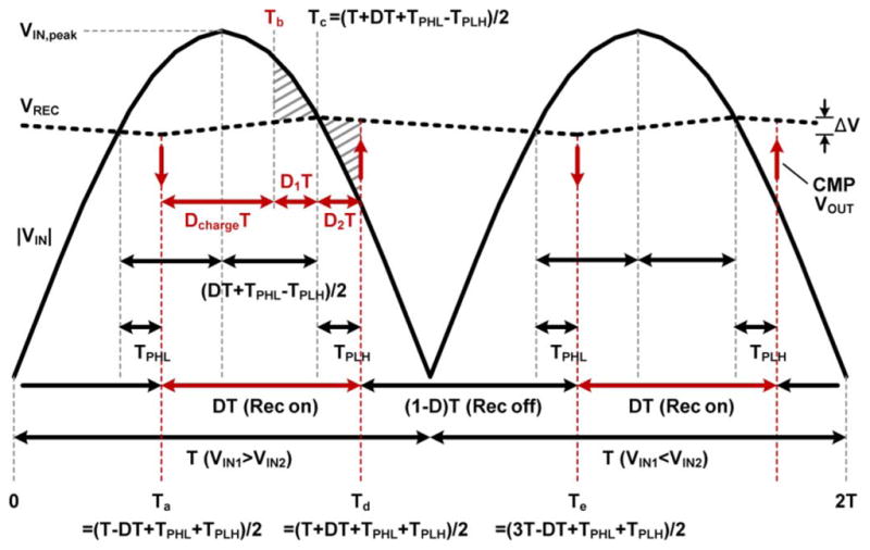
Simplified voltage waveforms of the active rectifier used in the PCE theoretical analysis. To simplify the equations, we have assumed ΔV → 0 V.
| (5) |
where Ta = (T–DT + TPHL + TpLH)/2, Td = (T + DT + TPHL + TPLH) 2, and Te = (3T – DT + TPHL + TPLH)/2 are indicated on Fig. 19. The sinusoidal input voltage, VIN, can be expressed as
| (6) |
Using (6) in (5), Ronp + Ronn can be expressed as a function of D
| (7) |
If TPLH = 0,. Dcharge would be the same as D because the rectifier only supplies RLCL during its conducting period. However, with TPLH > 0, the back current can discharge CL when VREC > |VIN|. In Fig. 19, the back current from Tc to Td(D2T) discharges CL as much as the forward current from Tb to Tc(D1T) charges CL. Therefore,. Dcharge can be derived as a function of D by obtaining Tb
| (8) |
| (9) |
By solving (5)–(9) for Tb using MATLAB, -Dcharge can be expressed as
| (10) |
Note that even though the input current from Tb to Td does not affect VREC, -Ron power losses still occur during this period (D1T + D2T). Therefore, the Ron loss term with Dcff in (2) can be represented as
| (11) |
where the first, second, and third terms of the right-hand side equation correspond to the Ron loss during DchargeT, D1T, and D2T, respectively. If TPLH = 0, the second and third terms will be eliminated because Tb = Tc = Td. Therefore, using (5)–(11), the Ron loss in (2) can be expressed as a function of D.
Ronp + Ronn can also be represented as a function of Wp = Wn
| (12) |
where Lmin is the length of the PMOS and NMOS transistors. By substituting Wp with (12), the switching loss term, PLoss,Cgp, in (2) can be expressed as a function of D
| (13) |
Therefore, by substituting (11) and (13) in (2) and differentiating it with respect to D, we can obtain the optimized D for minimum power loss inside the rectifier. Using the optimal D, the optimal Wp can be derived from (7) and (12), and the maximum PCE can be calculated from (4) by minimizing the power loss in (2).
Footnotes
Color versions of one or more of the figures in this paper are available online at http://ieeexplore.ieee.org.
References
- 1.Haddad SAP, Houben RPM, Serdijn WA. The evolution of pacemakers. IEEE Eng Med Biol Mag. 2006 May./Jun;25(3):38–48. doi: 10.1109/memb.2006.1636350. [DOI] [PubMed] [Google Scholar]
- 2.Ghovanloo M, Iniewski K, editors. VLSI Circuits For Biomedical Applications. Norwood, ma; Artech House: 2008. Integrated circuits for neural interfacing: Neural stimulation. [Google Scholar]
- 3.Finkenzeller K. RFID-Handbook. 2. Hoboken, NJ: Wiley; 2003. [Google Scholar]
- 4.Jow U, Ghovanloo M. Design and optimization of printed spiral coils for efficient transcutaneous inductive power transmission. IEEE Trans Biomed Circuits Syst. 2007 Sep;1(3):193–202. doi: 10.1109/TBCAS.2007.913130. [DOI] [PubMed] [Google Scholar]
- 5.Sauer C, Stanacevic M, Cauwenberghs G, Thakor N. Power harvesting and telemetry in CMOS for implanted devices. IEEE Trans Circuits Syst I, Reg Papers. 2005 Dec;52(12):2605–2613. [Google Scholar]
- 6.Ghovanloo M, Najafi K. Fully integrated wideband high-current rectifiers for inductively powered devices. IEEE J Solid-State Circuits. 2004 Nov;39(11):1976–1984. [Google Scholar]
- 7.Sawan M, Hu Y, Coulombe J. Wireless smart implants dedicated to multichannel monitoring and microstimulation. IEEE Circuits Syst Mag. 2005;5(1):21–39. [Google Scholar]
- 8.Ham JV, Puers R. A power and data front-end IC for biomedical monitoring systems. Sens Actuators A, Phys. 2008 Oct;147(2):641–648. [Google Scholar]
- 9.Ghovanloo M, Atluri S. An integrated full-wave CMOS rectifier with built-in back telemetry for RFID and implantable biomedical applications. IEEE Trans Circuits Syst I, Reg Papers. 2008 Nov;55(10):3328–3334. [Google Scholar]
- 10.Li P, Bashirullah R. A wireless power interface for rechargeable battery operated medical implants. IEEE Trans Circuits Syst II, Exp Briefs. 2007 Oct;54:912–916. [Google Scholar]
- 11.Le T, Han J, Jouanne A, Marayam K, Fiez T. Piezoelectric micro-power generation interface circuits. IEEE J Solid-State Circuits. 2006 Jun;41(6):1411–1420. [Google Scholar]
- 12.Nakamoto H, Yamazaki D, Yamamoto T, Kurata H, Yamada S, Mukaida K, Ninomiya T, Ohkawa T, Masui S, Gotoh K. A passive UHF RF identification CMOS tag IC using ferroelectric RAM in 0.35-,μm technology. IEEE J Solid-State Circuits. 2007 Jan;42:101–110. [Google Scholar]
- 13.Kotani K, Sasaki A, Ito T. High-Efficiency differential-drive CMOS rectifier for UHF rfids. IEEE J Solid-State Circuits. 2009 Nov;44(11):3011–3018. [Google Scholar]
- 14.Yoo J, Yan L, Lee S, Kim Y, Yoo H. A 5.2 mw self-configured wearable body sensor network controller and a 12 μW 54.9% efficiency wirelessly powered sensor for continuous health monitoring system. IEEE J Solid-State Circuits. 2010 Jan;45:178–188. [Google Scholar]
- 15.Lam YH, Ki WH, Tsui CY. Integrated low-loss CMOS active rectifier for wirelessly powered devices. IEEE Trans Circuits Syst II, Exp Briefs. 2006 Dec;53(12):1378–1382. [Google Scholar]
- 16.Bawa G, Ghovanloo M. Active high power conversionefficiency rectifier with built-in dual-mode back telemetry instandard CMOS technology. IEEE Trans Biomed Circuits Syst. 2008 Sep;2(3):184–192. doi: 10.1109/TBCAS.2008.924444. [DOI] [PubMed] [Google Scholar]
- 17.Hashemi S, Sawan M, Savaria Y. A novel low-drop CMOS active rectifier for RF-powered devices: Experimental results. Micro-electron J. 2009 Nov;40(11):1547–1554. [Google Scholar]
- 18.Guo S, Lee H. An efficiency-enhanced CMOS rectifier with unbalanced-biased comparators for transcutaneous-powered high-current implants. IEEE J Solid-State Circuits. 2009 Jun;44:1796–1804. [Google Scholar]
- 19.Guilar NJ, Amirtharajah R, Hurst PJ. A full-wave rectifier with integrated peak selection for multiple electrode piezoelectric energy harvests. IEEE J Solid-State Circuits. 2009 Jan;44:240–246. [Google Scholar]
- 20.Peters C, Spreemann D, Ortmanns M, Manoli Y. A CMOS integrated voltage and power efficient AD/DC converter for energy harvesting applications. J Micromech Microeng. 2008 Oct;18(10):104005–1104005. [Google Scholar]
- 21.Hwang Y, Lin H. A new CMOS analog front end for RFID tags. IEEE Trans Ind Electron. 2009 Jul;56(7):2299–2307. [Google Scholar]
- 22.Man TY, Mok PKT, Chan MJ. A 0.9-V input discontinuous-conduction-mode boost converter with CMOS-control rectifier. IEEE J Solid-State Circuits. 2008 Sep;43(9):2036–2046. [Google Scholar]
- 23.Sackinger E, Tennen A, Shulman D, Wani B, Rambaud M, Lim D, Larsen F, Moschytz GS. A 5-V ac-powered CMOS filter-selectivity booster for POTS/ADSL splitter size reduction. IEEE J Solid-State Circuits. 2006 Dec;41:2877–2884. [Google Scholar]
- 24.Bawa G, Ghovanloo M. Analysis, design and implementation of a high efficiency fullwave rectifier in standard CMOS technology. Analog Integr Circuits Signal Process. 2009 Aug;60:71–81. [Google Scholar]
- 25.Masui S, Ishii E, Iwawaki T, Sugawara Y, Sawada K. A 13.56-mhz CMOS RF identification transponder integrated circuit with a dedicated CPU. IEEE Int Solid-State Circuits Conf(ISSCC) Dig Tech Papers. 1999 Feb;:162–163. [Google Scholar]
- 26.Lee SB, Lee H, Kiani M, Jow U, Ghovanloo M. An inductively powered scalable 32-ch wireless neural recording system-on-a-chip with power scheduling for neuroscience applications. IEEE Trans Biomed Circuits Syst. 2010 Dec;4(6):360–371. doi: 10.1109/TBCAS.2010.2078814. [DOI] [PMC free article] [PubMed] [Google Scholar]
- 27.Kiani M, Ghovanloo M. An RFID-based closed-loop wireless power transmission system for biomedical applications. IEEE Trans Circuits Syst II, Exp Briefs. 2010 Apr;57:260–264. doi: 10.1109/TCSII.2010.2043470. [DOI] [PMC free article] [PubMed] [Google Scholar]
- 28.1N4148WT data sheet Diodes Inc [Online] Available: http://www.diodes.com/datasheets/ds30396.pdf.