Abstract
The bilayer graphene has attracted considerable attention for potential applications in future electronics and optoelectronics because of the feasibility to tune its band gap with a vertical displacement field to break the inversion symmetry. Surface chemical doping in bilayer graphene can induce an additional offset voltage to fundamentally affect the vertical displacement field and band-gap opening in bilayer graphene. In this study, we investigate the effect of chemical molecular doping on band-gap opening in bilayer graphene devices with single or dual gate modulation. Chemical doping with benzyl viologen molecules modulates the displacement field to allow the opening of a transport band gap and the increase of the on/off ratio in the bilayer graphene transistors. Additionally, Fermi energy level in the opened gap can be rationally controlled by the amount of molecular doping to obtain bilayer graphene transistors with tunable Dirac points, which can be readily configured into functional devices such as complementary inverters.
Keywords: graphene transistor, bilayer graphene, molecular doping, viologen, complementary inverter
Graphene is of considerable interest as a new electronic material for both fundamental investigations and potential applications due to its unique electronic properties including the exceptionally high carrier mobility and carrier saturation velocity.1–5 However, pristine graphene is a semimetal with zero bandgap and cannot be used for field effect transistors (FETs) with sufficient on/off ratio for digital electronic or photonic applications.6–8 A number of strategies have been proposed to create a bandgap in mono- or bilayer graphenes such as lateral quantum confinement9,10 and breaking the inversion symmetry in bilayer graphene.11–19 Both theoretical and experimental studies have demonstrated that a lateral confinement can be achieved in graphene nanoribbons or nanomeshes, to open up a transport band gap inversely proportional to the conducting channel width.20–23 However, a sizable gap can only be achieved at extremely narrow channel width (typically < 10 nm), which not only poses a serious technical challenge for conventional semiconductor processing but also causes severe degradation of the carrier mobility due to edge scattering effect.24–27
Bilayer graphene also has a gapless band structure. Interestingly, theoretical studies have suggested that a band gap can be opened in the Bernal-stacking (AB-stacking) bilayer graphene by applying an external electric filed normal to the graphene plane.12,28,29 This theoretical prediction has recently been experimentally verified in by optical measurements6,18,19 Electrical measurements have also demonstrated the opening a transport gap in the bilayer graphene with vertical displacement field.6,14–17 In particular, bilayer graphene FETs with on/off ratio up to 100 have been achieved in bilayer graphene devices at the room temperature,30 opening the promise for logic electronics. However, the high on/off ratio in such bilayer graphene devices is often achieved only with high voltage applied to both the top and bottom gates, and the Dirac point for the maximum on/off ratio state is not controlled and usually occurs at high bias point due to the fundamental requirement of large vertical displacement field. On the other hand, to apply such bilayer graphene device for possible complementary logic electronic applications, the control of the Dirac point is an import problem to address. Here we report the application of chemical molecular doping in bilayer graphene that can create an effective offset voltage to not only give rise additional displacement field for band gap opening, but also shift the Fermi energy level for tunable Dirac points. Threshold (Dirac point) split is demonstrated to achieve both n- and p-type bilayer graphene FETs for the construction of complimentary inverters.
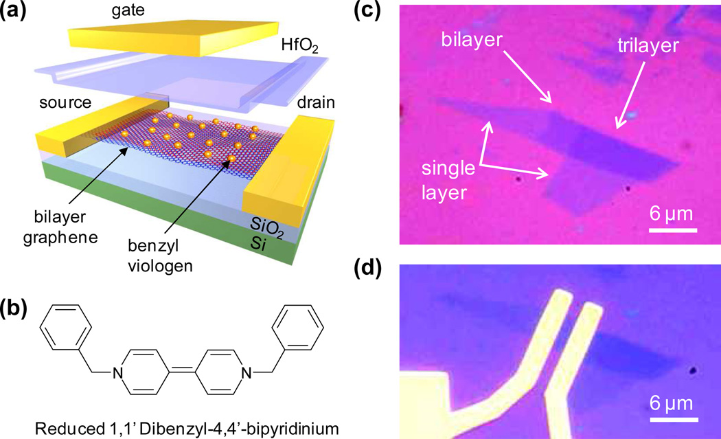
Figure 1a shows a schematic illustration of a dual gate bilayer graphene FET with surface molecular dopants. Reduced benzyl viologen molecules (BV) (Fig. 1b) are used as the dopants to control the surface doping effect in graphene. BV is known as an n-type dopant for carbon nanotubes (CNTs)31 because its lower reduction potential (−0.33 V) than that of CNTs (~0.23 V) to allow electron transfer from BV to CNTs. Similarly, coupling BV with graphene (with a reduction potential of ~0.22 V)32 can also result in an n-type doping effect. To fabricate the device, bilayer graphene was exfoliated from natural graphite and transferred onto a silicon substrate with a 300 nm silicon oxide layer. The bilayer graphene was identified based on their optical contrast (Fig. 1c) and confirmed with Raman spectroscopic studies.33 The source and drain electrodes (5-nm Cr/60-nm Au) were defined using conventional electron beam lithography process followed by a thermal evaporation metallization process (Fig. 1d). The BV molecular doping was applied by spin coating a toluene solution of the reduced BV onto the substrate followed by a hot plate baking process at 100 ° for 1 minute. The amount of dopants can be controlled by the number of successive spin coating processes.
Figure 1.
(a) The schematic illustration of the benzyl viologen doped bilayer graphene dual-gate transistor. From top to bottom: top-gate electrode (Cr/Au), top-gate dielectric (50 nm HfO2), benzyl viologen doped bilayer graphene with source and drain electrodes (Cr/Au), 300 nm SiO2 bottom-gate oxide, and silicon bottom-gate. (b) Molecular structure of the reduced benzyl viologen molecule. (c) Optical microscopy images of an exfoliated graphene flake and (d) the corresponding bilayer graphene FET. The arrows in (c) indicate single layer, bilayer, and trilayer graphene sheets.
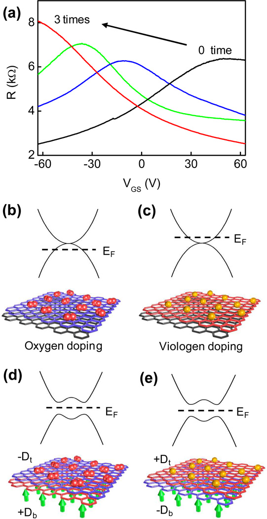
The unintentionally doped graphene typically exhibit a p-type transistor characteristic with a highly positive Dirac point, likely due to an oxygen doping effect.34 The Dirac point can be readily tuned by applying surface molecular dopants such as BV molecules. Electrical measurements show that the application of BV onto graphene surface produces an expected n-type doping effect to create a negative shift in Dirac points in single bottom-gated device with increasing amount of BV doping (Fig. 2a).31 The threshold voltage (Dirac point) was in the positive gate voltage regime (~ +50 V) with a p-type characteristics before BV doping (black line, Fig. 2a). The threshold voltage was shifted to near the ~ −10 V and the on/off ratio was decreased upon the first application of BV doping process (blue line, Fig. 2a). The second and the third applications of BV dopants further shift the threshold voltage toward increasingly negative gate voltage points (~ −37 V, and ~ −60 V) and the on/off ratio is also improved with increasing dopant amount (green and red line, Fig. 2a). Similar effects have also been observed recently in single bottom-gated bilayer graphene devices with surface adsorbate dopants.35
Figure 2.
(a) The switching behavior as a function of bottom-gate voltage with various benzyl viologen doping amount in single bottom-gated bilayer graphene device. Energy band structure and doping schematics of of bilayer graphene with (b) top layer p-doped by oxygen, (c) top layer n-doped by benzyl viologen, (d) additional bottom layer n-doped by a positive bottom-gate voltage, and (e) additional bottom layer p-doped by a negative bottom-gate voltage.
The above observations can be explained by displacement equations. In a typical dual gate device with both the top- and bottom-gate, the top displacement field (Dt) and bottom displacement field (Db) are produced by applying dual gate bias. The average of the two displacement field, D̅ = (Db + Dt) / 2, breaks the inversion symmetry of the bilayer graphene and generates a non-zero band gap.6 The deference of the two displacement field, δD = Db − Dt, shifts the Fermi energy (EF) and creates a net carrier doping. At the point of δD = 0 called ‘charge neutral points’ (CNPs, also known as Dirac point in graphene), Fermi level is located at the middle of conduction band edge and valence band edge and the resistance is maximized. In general, displacement field (D) can be described using the relationship: and , which show that the displacement field is tuned not only by the gate voltages (Vt and Vb) but also by the effective offset voltage ( and ) which are produced by chemical dopants. Here ε and d are the dielectric constant and thickness of the dielectric layer. Since the surface molecular doping (by the BV molecules or oxygen molecules) predominantly affects the top layer of bilayer graphene, the effective offset voltage () of top layer is changed and effective offset voltage () of bottom layer largely keeps a constant charge doping during the chemical doping process, neglecting spontaneous transfer of charges between two layers. In this way, the molecular dopants themselves induce a top layer effective offset voltage () to produce the total top displacement field (Dt ) without an actual top gate. In Figure 2a, the Dirac point of the device without intentional molecular doping is +50 V (due to unintentional oxygen doping effect from the environment), corresponding to Db ≈ 0.65 Vnm−1 considering εb = 3.9 and db = 300 nm for thermal SiO2. Because two displacement fields have same value (Db = Dt) at the Dirac point, the top displacement field is Dt ≈ 0.65 Vnm−1. With increasing BV doping, the Dirac point changed to −10 V, −37 V, −60 V and the corresponding top displacement field Dt changed to the −0.13 Vnm−1, −0.48 V nm−1, and −0.78 V nm−1, respectively.
In this way, before BV doping, oxygen doping produces a positive displacement field Dt ≈ 0.65 Vnm−1 with Fermi level located at lower valence band (Fig. 2b) and the corresponding threshold voltage (Dirac point) located in the positive voltage regime (Fig. 2a). With increasing BV doping, the top displacement fields (Dt) are changed to −0.13 Vnm−1, −0.48 V nm−1, and −0.78 V nm−1 for 1, 2 and 3 times of doping processes, respectively. The corresponding Fermi level moves upward (Fig. 2c) and threshold voltage moves to negative gate voltage regime (Fig. 2a). The band gap is tuned by the amount of displacement field. The averages of the two displacement field (D̅) at the Dirac point are 0.65 Vnm−1, −0.13 Vnm−1, −0.481 V nm−1, and −0.78 V nm−1 with 0, 1, 2 and 3 times of doping processes, respectively. Before doping, top displacement field produced by oxygen doping along with bottom displacement filed by produced by the bottom gate voltage breaks the inversion symmetry of the bilayer to create a non-zero band gap (Fig. 2d). At the first doping process, hole carriers from oxygen are neutralized by electrons from BV and it reduces the top displacement field and band gap. After the second doping, the number of electron carriers increases with increasing BV doping, leading to an increase in the amplitude of the top displacement field, which together with bottom displacement field opens a finite or transport band gap in the bilayer graphene devices (Fig. 2e). As a result, the on/off ratio is reduced at the first BV doping and increased after the second and third BV doping (Fig. 2a).
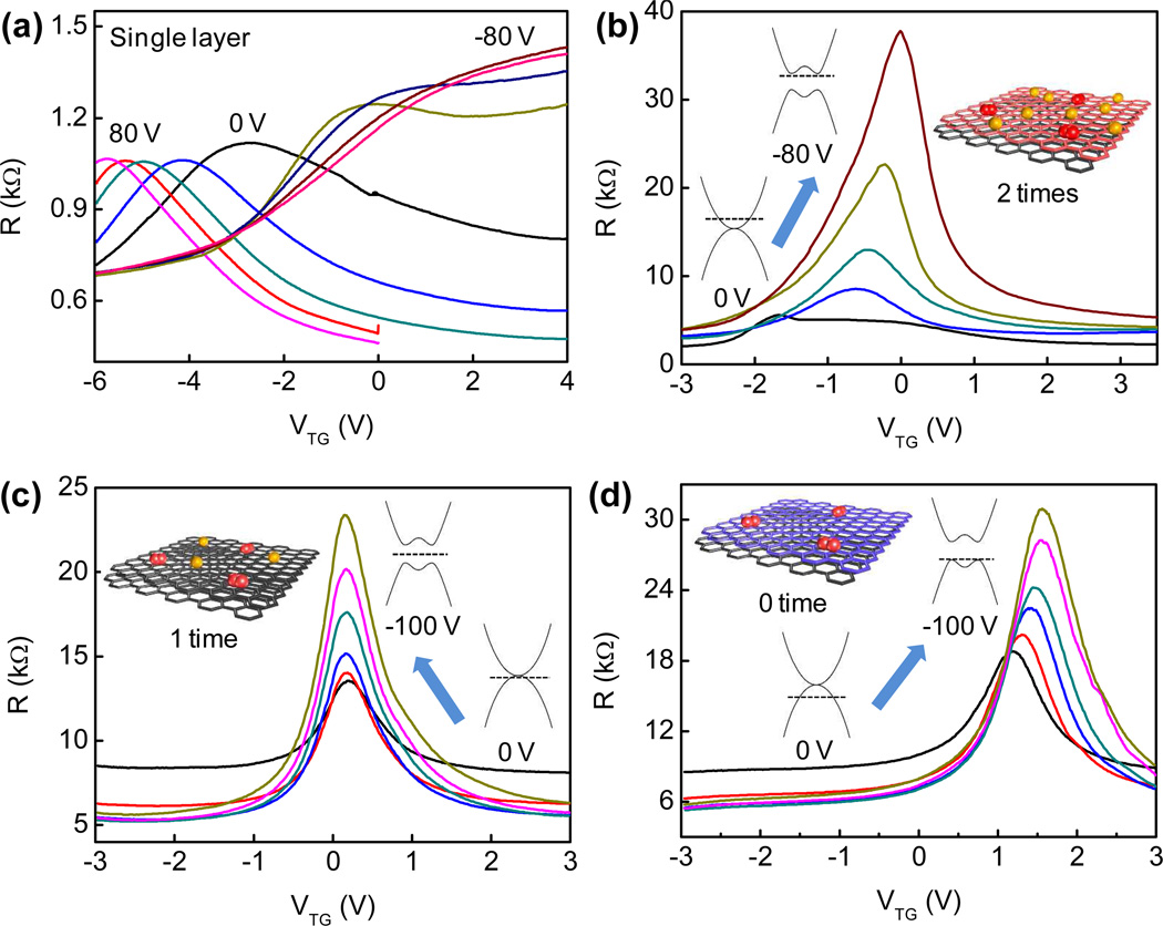
The molecular doping effect can be readily employed to tune the Dirac points of the dual-gated bilayer graphene devices (Fig. 3). For the dual gate structure, the HfO2 (50nm) and Cr (5nm)/Au (60nm) thin film were deposited as the top gate dielectric and top gate electrode with an e-beam evaporation process.36 The switching characteristics of the dual gate graphene FETs were characterized by sweeping top-gate voltage at fixed bottom-gate voltages. As expected, the dual gate device made from single layer graphene shows little change in on/off ratio as the back gate voltage is changed from −80 V to 80 V, with a maximum on/off ratio around 2 or so (Fig. 3a). In contrast, the on/off ratio of all bilayer graphene devices are improved significantly as back gate voltage is increased from 0 V to −80 V, with a maximum on/off ratio exceeding 10 (Fig. 3b–d), signifying the opening of a transport gap opening in bilayer graphene with vertical displacement field.
Figure 3.
(a) The dual-gate switching characteristics of a single layer graphene FET as a function of top-gate voltage at different fixed bottom-gate voltages and (b–d) the dual-gate switching characteristics of bilayer graphene FET with (b) 2 times, (c) 1 time, and (d) 0 time application of benzyl viologen doping on graphene. Bottom-gate modulation steps are 20 V. The insets in (b–d) show the schematics of doping and the corresponding energy band structures before and after band gap opening.
In order to further confirm the BV doping effect, the switching characteristics of dual-gated bilayer graphene devices were studied with variable doping amount (Fig. 3b–d). Without applying bottom gate voltage, the initial threshold voltages (Dirac points) of the top-gated devices with 2, 1 and 0 times of doping processes were −1 V, 0.15 V, and 1.18 V, respectively. After applying a negative bottom-gate voltage to open the transport gap and achieve improved on/off ratio, the threshold voltages were changed to −0.01V, 0.17 V, and 1.56 V for the device with 2, 1 and 0 times of doping processes, respectively. With increasing BV doping amount, the top-gate Diract points shift towards the negative voltage direction, suggesting the upward shift of the Fermi level from lower valence band to upper conduction band with increasing net electron doping (insets of Fig. 3b–d). The application of additional negative bottom-gate voltage opens the band gap and changes the net carrier doping. The on/off ratios were increased and top-gate threshold voltages were slightly shifted to positive direction as well. The threshold voltage differences achieved in devices with different doping amount were largely retained during the dual-gate modulation and gap opening process.
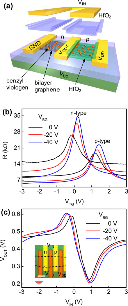
The ability to achieve high on/off ratio bilayer graphene devices with tunable threshold voltage (Dirac point) readily allows the construction of functional devices such as complementary inverter using dual-gated p- and n-type bilayer graphene FETs. Figure 4a illustrates the schematics of a complementary inverter constructed using both p-type and n-type bilayer graphene devices fabricated on the same graphene flake. Specifically, two intrinsically p-doped graphene FETs were first fabricated on the same bilayer graphene in series, with one of the FET selectively converted into n-type using BV doping. For selective BV doping, one FET was first covered by a 10-nm HfO2 protecting layer using an e-beam lithography and e-beam evaporation deposition process. BV molecules were then spin-coated onto the substrate to render the uncovered FET n-type. Finally, the top-gate dielectric (HfO2 50 nm) and top-gate electrode (Cr 5nm/Au 60nm) were deposited. Electrical measurements of switching characteristics of the two bilayer graphene FETs show distinct Dirac points (Fig. 4b), as a result of selectively doping one FET only. As discussed above (Fig. 3b–d), the on/off ratio of both p- and n-type bilayer graphene devices increases with increasing the negative back gate voltage, while threshold voltage difference is roughly maintained. Figure 4c shows electrical switching characteristics of the complementary inverter assembled by using n- and p-type bilayer FETs. Supply voltage (VDD) of 1V was applied to the right electrode of p-type bilayer FET and the left electrode of n-type bilayer FET was grounded. Output voltage (VOUT) was measured with varying input voltage (VIN). Two output voltage peaks were observed near the 0 V and the 1 V, around the Dirac points of the two FETs. According to the voltage division between the p- and n-type FETs, the upper peak appears near the off state of n-type FET and lower peak shows at the off state of p-type FET. With increasing bottom-gate voltage, the off resistance of each FET increases, which in turn improves the on/off ratio of inverter output voltage.
Figure 4.
(a) The schematic illustration of a complementary inverter. (b) The switching behavior of an n-type (BV doped) and a p-type (undoped) bilayer graphene FET as a function of top-gate voltage at different bottom-gate voltages. (c) The electrical switching characteristics (at various bottom-gate voltages) of a complementary inverter assembled by connecting an n- and a p-type bilayer graphene FET together. The inset shows an optical image of a complementary bilayer graphene inverter. Scale bar is 5µm.
In summary, we have demonstrated that chemical molecular doping can produce an additional displacement field to facilitate the opening of a transport gap in bilayer graphene and to tune Dirac points (threshold voltage) in single and dual-gated graphene FETs. Complementary inverter was assembled using bilayer graphene FETs with split thresholds. The on/off ratio of the inverter can be tune by the perpendicular electrical field. Our study for the first time demonstrates the exciting potential in exploring the molecular doping to rationally tune the electronic properties of bilayer graphene devices for functional circuits.
Acknowledgments
We acknowledge the Nanoelectronics Research Facility (NRF) and the Center for High Frequency Electronics (CHFE) at UCLA for technical support. X.D. acknowledges support by NSF CAREER award 0956171 and by the NIH Director's New Innovator Award Program, part of the NIH Roadmap for Medical Research, through Grant 1DP2OD004342-01.
References
- 1.Novoselov KS, Geim AK, Morozov SV, Jiang D, Zhang Y, Dubonos SV, Grigorieva IV, Firsov AA. Science. 2004;306:666. doi: 10.1126/science.1102896. [DOI] [PubMed] [Google Scholar]
- 2.Novoselov KS, Geim AK, Morozov SV, Jiang D, Katsnelson MI, Grigorieva IV, Dubonos SV, Firsov AA. Nature. 2005;438:197. doi: 10.1038/nature04233. [DOI] [PubMed] [Google Scholar]
- 3.Dean CR, Young AF, Meric I, Lee C, Wang L, Sorgenfrei S, Watanabe K, Taniguchi T, Kim P, Shepard KL, Hone J. Nat. Nanotechnol. 2010;5:722. doi: 10.1038/nnano.2010.172. [DOI] [PubMed] [Google Scholar]
- 4.Wu YQ, Lin YM, Bol AA, Jenkins KA, Xia FN, Farmer DB, Zhu Y, Avouris P. Nature. 2011;472:74. doi: 10.1038/nature09979. [DOI] [PubMed] [Google Scholar]
- 5.Liao L, Lin YC, Bao MQ, Cheng R, Bai JW, Liu YA, Qu YQ, Wang KL, Huang Y, Duan XF. Nature. 2010;467:305. doi: 10.1038/nature09405. [DOI] [PMC free article] [PubMed] [Google Scholar]
- 6.Zhang Y, Tang T, Girit C, Hao Z, Martin MC, Zettl A, Crommie MF, Shen YR, Wang F. Nature. 2009;459:820. doi: 10.1038/nature08105. [DOI] [PubMed] [Google Scholar]
- 7.Wang F, Zhang Y, Tian H, Girit C, Zettl A, Crommie M, Shen YR. Science. 2008;320:206. doi: 10.1126/science.1152793. [DOI] [PubMed] [Google Scholar]
- 8.Xia F, Mueller T, Lin Y-M, Valdes-Garcia A, Avouris Ph. Nat. Nanotechnol. 2009;4:839. doi: 10.1038/nnano.2009.292. [DOI] [PubMed] [Google Scholar]
- 9.Nakada K, Fujita M, Dresselhaus G, Dresselhaus MS. Phys. Rev. B. 1996;54:17954. doi: 10.1103/physrevb.54.17954. [DOI] [PubMed] [Google Scholar]
- 10.Wakabayashi K, Fujita M, Ajiki H, Sigrist M. Phys. Rev. B. 1999;59:8271. [Google Scholar]
- 11.McCann E, Falko V. Phys. Rev. B. 2006;74:161403(R). [Google Scholar]
- 12.Castro EV, Novoselov KS, Morozov SV, Peres NMR, Lopes dos Santos JMB, Nilsson J, Guinea F, Geim AK, Neto AHC. Phys. Rev. Lett. 2007;99:216802. doi: 10.1103/PhysRevLett.99.216802. [DOI] [PubMed] [Google Scholar]
- 13.McCann E, Falko V. Phys. Rev. Lett. 2006;96:086805. doi: 10.1103/PhysRevLett.96.086805. [DOI] [PubMed] [Google Scholar]
- 14.Zou K, Zhu J. Phys. Rev. B. 2010;82:081407. [Google Scholar]
- 15.Jing L, Velasco J, Jr, Kratz P, Liu G, Bao W, Bockrath M, Lau CN. Nano Lett. 2010;10:4000. doi: 10.1021/nl101901g. [DOI] [PubMed] [Google Scholar]
- 16.Taychatanapat T, Jarillo-Herrero P. Phys. Rev. Lett. 2010;105:166601. doi: 10.1103/PhysRevLett.105.166601. [DOI] [PubMed] [Google Scholar]
- 17.Yan J, Fuhrer MS. Nano Lett. 2010;10:4521. doi: 10.1021/nl102459t. [DOI] [PubMed] [Google Scholar]
- 18.Li ZQ, Henriksen EA, Jiang Z, Hao Z, Martin MC, Kim P, Stormer HL, Basov DN. Phys. Rev. Lett. 2009;102:037403. doi: 10.1103/PhysRevLett.102.037403. [DOI] [PubMed] [Google Scholar]
- 19.Zhang LM, Li ZQ, Basov DN, Fogler MM. Phys. Rev. B. 2008;78:235408. [Google Scholar]
- 20.Han MY, Ozyilmaz B, Zhang Y, Kim P. Phys. Rev. Lett. 2007;98:206805. doi: 10.1103/PhysRevLett.98.206805. [DOI] [PubMed] [Google Scholar]
- 21.Li X, Wang X, Zhang L, Lee S, Dai H. Science. 2008;319:1229. doi: 10.1126/science.1150878. [DOI] [PubMed] [Google Scholar]
- 22.Chen Z, Lin Y-M, Rooks MJ, Avouris Ph. Physica E. 2007;40:228. [Google Scholar]
- 23.Bai J, Duan X, Huang Y. Nano Lett. 2009;9:2083. doi: 10.1021/nl900531n. [DOI] [PubMed] [Google Scholar]
- 24.Li X, Wang X, Zhang L, Lee A, Dai H. Science. 2008;319:1229. doi: 10.1126/science.1150878. [DOI] [PubMed] [Google Scholar]
- 25.Bai J, Zhong X, Jiang S, Huang Y, Duan X. Nat. Nanotechnol. 2010;5:190. doi: 10.1038/nnano.2010.8. [DOI] [PMC free article] [PubMed] [Google Scholar]
- 26.Jiao L, Zhang L, Wang X, Diankov G, Dai H. Nature. 2009;458:877. doi: 10.1038/nature07919. [DOI] [PubMed] [Google Scholar]
- 27.Kosynkin DV, Higginbotham AL, Sinitskii A, Lomeda JR, Dimiev A, Price BK, Tour JM. Nature. 2009;458:872. doi: 10.1038/nature07872. [DOI] [PubMed] [Google Scholar]
- 28.Gava P, Lazzeri M, Saitta AM, Mauri F. Phys. Rev. B. 2009;79:165431. [Google Scholar]
- 29.Ohta T, Bostwick A, Seyller Th, Horn K, Rotenberg E. Science. 2006;313:951. doi: 10.1126/science.1130681. [DOI] [PubMed] [Google Scholar]
- 30.Xia F, Farmer DB, Lin Y, Avouris Ph. Nano Lett. 2010;10:715. doi: 10.1021/nl9039636. [DOI] [PubMed] [Google Scholar]
- 31.Kim SM, Jang JH, Kim KK, Park HK, Bae JJ, Yu WJ, Lee IH, Kim G, Loc DD, Kim UJ, Lee E-H, Shin H-J, Choi J-Y, Lee YH. J. Am. Chem. Soc. 2009;131:327. doi: 10.1021/ja807480g. [DOI] [PubMed] [Google Scholar]
- 32.Kim KK, Reina A, Shi Y, Park H, Li L-J, Lee YH, Kong J. Nanotechnol. 2010;21:285205. doi: 10.1088/0957-4484/21/28/285205. [DOI] [PubMed] [Google Scholar]
- 33.Blake P, Hill EW, Neto AHC, Novoselov KS, Jiang D, Yang R, Booth TJ, Geim AK. Appl. Phys. Lett. 2007;91:063124. [Google Scholar]
- 34.Ryu S, Liu L, Berciaud S, Yu Y-J, Liu H, Kim P, Flynn GW, Brus LE. Nano Lett. 2010;10:4944. doi: 10.1021/nl1029607. [DOI] [PubMed] [Google Scholar]
- 35.Szafranek BN, Schall D, Otto M, Neumaier D, Kurz H. Nano Lett. 2011;11:2640. doi: 10.1021/nl200631m. [DOI] [PubMed] [Google Scholar]
- 36.Bai J, Liao L, Zhou H, Cheng R, Lixin L, Huang Y, Duan X. Nano Lett. 2011;11:2555. doi: 10.1021/nl201331x. [DOI] [PMC free article] [PubMed] [Google Scholar]


