Abstract
Graphene transistors are of considerable interest for radio frequency (RF) applications. In general, transistors with large transconductance and drain current saturation is desirable for RF performance, which is however nontrivial to achieve in graphene transistors. Here we report high performance top-gated graphene transistors based on chemical vapor deposition (CVD) grown graphene with large transconductance and drain current saturation. The graphene transistors were fabricated with evaporated high dielectric constant material (HfO2) as the top-gate dielectrics. Length scaling studies of the transistors with channel length from 5.6 µm to 100 nm shows that complete current saturation can be achieved in 5.6 µm devices and the saturation characteristics degrade as the channel length shrinks down to 100–300 nm regime. The drain current saturation was primarily attributed to drain bias induced shift of the Dirac points. With the selective deposition of HfO2 gate dielectrics, we have further demonstrated a simple scheme to realize a 300 nm channel length graphene transistors with self-aligned source-drain electrodes to achieve the highest transconductance of 250 µS/µm reported in CVD graphene to date.
Keywords: Graphene, transistors, dielectrics, current saturation, self-alignment
Graphene exhibits many unique characteristics, including the highest carrier mobility, the highest carrier saturation velocity and highest thermal conductivity, that make it an attractive electronic material for ultra high-speed radio frequency applications.1–7 In particular, graphene transistors with maximum cut-off frequency exceeding 100 GHz have been recently demonstrated using epitaxial graphene or CVD grown graphene.6–7 This exceptional performance advancement is achieved by continued shrinking the transistor channel length. However, the performance of these devices is still at least partly limited by the presence of access resistance due to the gaps exist between the source-gate and gate-drain electrodes. In the state-of-art silicon metal-oxide-semiconductor field-effect transistor (MOSFET) technology, a self-aligned gate structure is used to ensure the precise positioning of source, drain and gate electrode to reduce the gaps and overlaps between gate and source or drain in order to simultaneously minimize the access resistance and parasitic capacitance for desired transistor performance. However, the traditional fabrication processes in silicon MOSFET technology cannot be readily applied to graphene transistors due to the difficulties associated with selective deposition and pattern of dielectric materials on graphene without degrading the structure or electronic performance of graphene. A self-aligned process has recently been developed using synthetic metal/dielectric core/shell nanowires as the gate, and enabled graphene transistors with cut-off frequency reaching 300 GHz or higher.4,8 The scalable fabrication of graphene transistors using this approach, however, is complicated with the usage of the mechanically peeled graphene flakes and the requirement of unconventional nanowire assembly process. It therefore remains a significant challenge to realize short channel transistors for high frequency applications due to the difficulties in selective patterning the dielectric layer on grapheme in large scale. Additionally, the transistors reported in these previous efforts showed little drain current saturation, which is undesirable for power gain performance.9 Although drain current saturation has been reported in phonon scatter limited velocity saturation regime using exfoliated graphene or with h-BN as the back gate dielectrics,10–13 it has not been reported in CVD graphene to date.
To address these challenges, here we report our effort in exploring an evaporation process that can allow for selective deposition of a high-dielectric constant (high-k) dielectric layer on large area CVD graphene enabling the self-aligned fabrication of graphene transistors. Importantly, high performance top-gated CVD graphene transistors have been fabricated with clear drain current saturation. Self-aligned graphene transistor is fabricated with a record high transconductance of 250 µS/µm obtained in CVD graphene device. Using a conventional lithography and CVD grown graphene, this process opens opportunity for the large scale fabrication of high performance graphene transistors.
The graphene transistors studied here consist of CVD grown graphene as the channel material, Pd/Au thin film as the source and drain electrodes, and HfO2/Ti/Au as the top gate stack (Fig. 1). To make the device, high quality single layer graphene was grown on Cu foil based on an ambient pressure CVD method (supplementary materials) and transferred onto silicon substrate (with 300 nm SiO2 on top).14,15 The graphene was then patterned into strips with desired width through a photolithography and oxygen plasma etching process. The source-drain electrodes were next defined by e-beam lithography followed by e-beam evaporation deposition of Pd/Au (10/30 nm) thin film. After forming the contact electrodes, a 40 nm HfO2 film was evaporated onto the graphene substrate as the top gate dielectrics by e-beam evaporation.16 The dielectric constant of evaporated HfO2 thin film was measured to be ~ 19 (Fig. S2), comparable to the reported values for e-beam evaporated HfO2.17–19 The top-gate electrode was subsequently formed by e-beam lithography patterning and metallization process (Ti/Au). Devices with different channel length (L) were fabricated to study the channel length scaling behavior. To investigate the basic device performance, the grapheme transistors were fabricated with complete gate to source or drain overlapping to minimize the access resistance.
Figure 1.
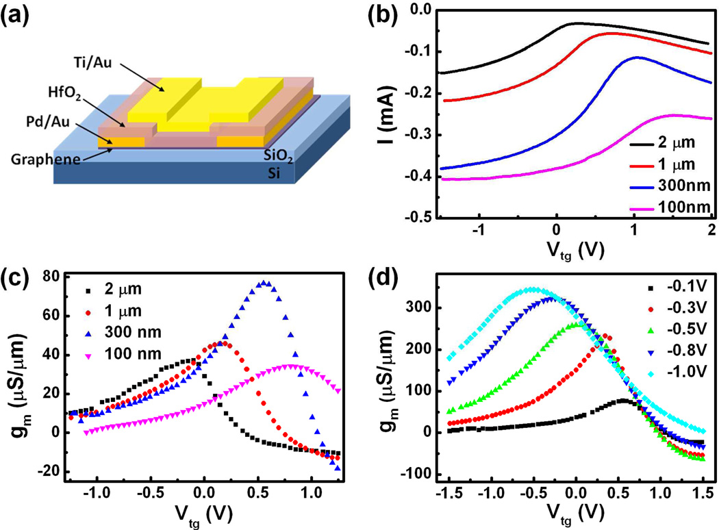
(a) Schematic illustration of the device structure of top gated graphene transistors for the evaluation of the channel length scaling effect. (b) Transfer characteristics of top-gated graphene transistor at Vds=−0.1V with channel lengths 2 µm, 1 µm, 300 nm and 100 nm. The channel width is 3.4 µm for all devices. (c) The corresponding transconductance of the devices shown in (b) at Vds=−0.1V. (d) The evolution of transconductance with gate voltage for the 300 nm channel device at bias voltage −0.1V, −0.3V, −0.5V, −0.8V and −1.0V.
Figure 1b depicts the representative transfer characteristics with channel length ranging from 2 µm to 100 nm. The devices show typical characteristics of p-type doping and electron-hole asymmetry in which the Dirac points are located at positive gate voltage with a suppression of electron conduction branch. The p-type doping is attributed to oxygen doping during graphene growth and transfer process, and the electron-hole asymmetry is likely originated from imbalanced carrier injection caused by misalignment between the contact electrode work function and channel neutrality points.20 The hole transport branches switch from saturation to current minimum in a gate voltage span of about 2 V. A general trend of positive shift of Dirac point and decrease of on-off ratio is observed with the decrease of channel length. This can be explained as a short channel effect: in short channel device, where the channel potential is strongly affected by the drain potential, a more opposite voltages is needed to turn off the channel.21 Similar to the silicon p-MOSFETs short channel threshold roll-off, in graphene FETs when current carriers are holes, a more positive voltage is needed to reach the current minimum, leading to a positive shift of Dirac point with down scaling of the channel length. On the other hand, the transconductance in shorter channel device increases due to the reduction of channel resistance. The peak transconductance at bias of 100 mV increases from 36 µS/µm (L=2 µm) to 77 µS/µm (L=300 nm) (Fig. 1c). However, a further shrinkage of channel length to 100 nm results in a reduction of peak transconductance to 34 µS/µm, due to a short channel effect.21 The transconductance is also highly dependent on the drain voltage. The measured largest transconductance is 350 µS/µm obtained at L=300 nm and Vds of −1 V (Fig. 1d).
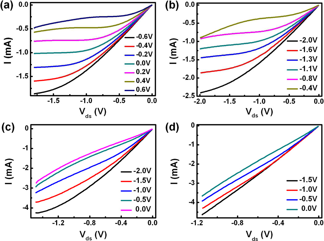
Interestingly, our fabricated graphene transistors show clear drain current saturation at relative low voltage (−1 V to −1.4 V) (Fig. 2). A full current saturation is achieved in a long channel device (L=5.6 µm), exhibiting near zero drain source conductance (gds) (< 2 µS/µm) in the saturation region (Fig. 3a, S3). The gds is about 47 µS/µm for L=2 µm device and 65 µS/µm for L=300 nm channel device (Vds=1.4 V and Vg=−2 V). Little saturation is found when L shrinks down to 100 nm. A important figure-of-merit in analog amplifiers is evaluated by intrinsic gain (gm/gds) which represents the theoretical maximum gain achievable by a single transistor.9 Previously reported graphene RF devices show little drain saturation with a relatively large drain conductance and low intrinsic gain typically smaller than unit, making it less interesting for practical amplifier applications. In our case, the intrinsic gain for L=5.6 µm device is estimated to be larger than 50 (at Vds=−1.3 V, Vg=0.2 V). This value drops to 7 for L=2 µm and to about 4 for L=300 nm devices. Although similar current saturation was previously reported in graphene devices made by high quality exfoliated graphene,10–13 our work demonstrated for the first time that current saturation can also been achieved in devices produced on CVD grown graphene, making it possible for large scale fabrication of graphene devices with desirable intrinsic gain.
Figure 2.
Output characteristics showing the current saturation behavior for devices with variable channel lengths: (a) L=5.6 µm, (b) 2 µm, (c) 300 nm, and (d) 100 nm.
Figure 3.
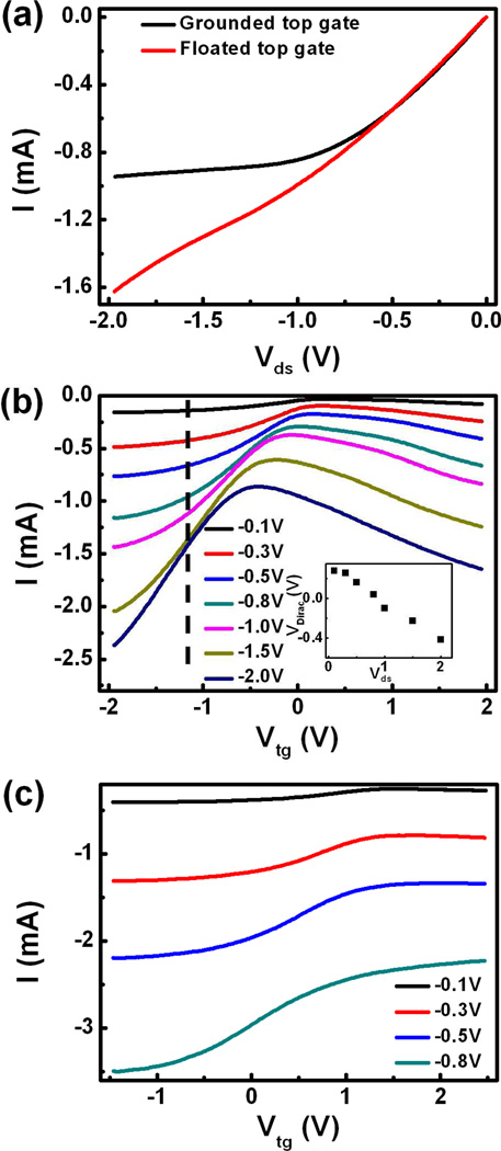
(a) I–V characteristic of a long channel device (L=5.6 µm) under grounded or floated gate condition. (b) Transfer characteristic at different bias voltage for the device with L=2 µm. The inset shows Dirac point shift as a function of bias voltage. (c) Transfer characteristic at different bias voltage for the device with L=100 nm.
To further probe the origin of the saturation behavior in our graphene transistors, we focus on a device showing good p-type doping and saturation characteristics at zero gate (gate grounded at zero bias) (black curve in Fig. 3a). Interestingly, no clear current saturation is observed in the same device when the gate electrode is floated, suggesting that the current saturation observed here is likely due to the relative potential between the drain and gate (ie: bias induced additional gating effect), rather than the intrinsic velocity saturation associated with phonon scattering. In field-effect transistors, bias voltage alters the channel potential in a way equivalent to a gate voltage with opposite sign coupled through the oxide. In analogy to the pinch-off behavior in silicon device, a negative bias in graphene transistor creates a relative positive potential in the gate (in reference to the drain) to deplete the holes at the drain end, and current saturation is observed when the minimal carrier density is reached. Usually, a good gate coupling (large Cox) is needed in order to achieve saturation at relative low bias voltage, which we can achieve with the evaporated high-k dielectrics. The pinch-off effect has also been evaluated in exfoliated graphene FETs by Meric et. al., where the observed current saturation was attributed to phonon scattering induced velocity saturation.10 Additionally, the gds rise up with further increase Vds beyond the saturation voltage, produce a current kink in the I–Vds curve.22-24 It can be explained by the formation of additional electron conduction channel at the drain end as the pinch-off point moves into the channel. The current kink is a unique characteristic for ambipolar transistors. Similar results were also found in carbon nanotube ambipolar transistors.22–24
The drain bias induced gating effect can be better viewed by observing the shift of Dirac point with different drain bias voltages. As shown in a family I–Vg curves with different drain bias Vds (Fig. 3b), the increase of negative Vds not only increases the overall current, but also shifts the curves to negative voltage direction. In conjunction with the sharp switching of hole transport branch, the I–Vtg curves at different bias voltage grow closer to each other with the increase of negative Vds so that the drain current saturation can be reached (for example, along the dash line in Fig. 3b). In ambipolar transistors, a current minimum point is reached when electron/hole current injected from source/drain is balanced with each other, in equivalent to hold the Dirac point at zero gate voltage and apply equal and opposite voltage (±1/2Vds) to source and drain. Therefore, the gate-source or gate-drain potential difference, which is also the Dirac point voltage when either the source or drain are grounded, will shift by 1/2ΔVds with a change of bias voltage ΔVds. In our long channel device, the Dirac point shifts approximately −0.7 V when Vds increase from −0.1 V to −2 V (Fig. 3b and inset), close to the theoretical prediction. Similar effect was reported in ambipolar graphene or carbon nanotube FETs.21,22–24 On the other hand, when channel length shrinks down to 100 nm, the short channel effect starts to dominate. As discussed above, the short channel effect will move the Dirac point to the opposite side of applied bias, leading to a positive shift of Dirac point with a negative Vds. As a result, the Dirac point shifts to positive voltage at L=100 nm and no current saturation is observed (Fig. 3c, 2d). This also explains the observation of weak saturation at L=300 nm.
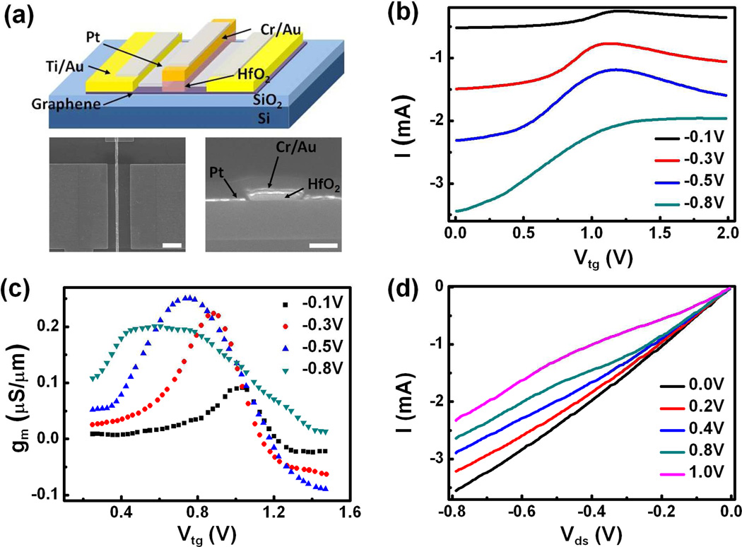
Selective deposition of HfO2 dielectric layer on CVD graphene can allow for the fabrication of the self-aligned graphene devices (Fig. 4a). To fabricate the device, a narrow strip of the gate stack (HfO2/Cr/Au: 40 nm/4 nm/20 nm) is first defined on graphene by one step e-beam lithography followed by vacuum deposition and lift-off processes. After the formation of the gate stack, a thin layer of Pt (10 nm) is deposited on top of graphene and across the pre-formed gate stack, in which the gate stack separate the Pt thin film into two separated pads as the self-aligned source and drain electrodes (Fig. 4a). The transport measurement shows only slight saturation in the output characteristics (Fig. 4d), likely due to the short channel effect. The transfer characteristics are similar to devices described above. The device shows an on-off ratio of 2 within a full on-off swing in the gate range of 0–1.5 V. The self-aligned structure can enable small access resistance to ensure a large delivery current up to 0.44 mA/µm at Vds=−0.8 V and Vg=0.8 V. The transconductance reaches 250 µS/µm at Vds=−0.5 V, and degrades with further increase in bias voltage. To the best of our knowledge, the scaled on-current and transconductance obtained here represents the highest value among the reported CVD graphene transistors.
Figure 4.
(a) Schematic (top), top view (bottom left) and cross section (bottom right) SEM image of a typical self-aligned device. The scale bar indicates 2 µm in the top view SEM image, and 200nm in the cross section SEM image. (b) Transfer characteristic and (c) corresponding transconductance under different bias voltage for an L=300 nm self-aligned device. (d) Output characteristics of the same device.
In conclusion, we have shown that high performance transistor can be obtained by using the CVD graphene as the channel and the evaporated HfO2 as the gate dielectrics. A drain current saturation can be achieved in graphene transistors with channel length down to 300 nm, which was attributed to the bias induced shift of the Dirac point. We have also demonstrated a simple scheme to realize a self-aligned gate structure with the best transconductance reported for CVD graphene transistor to date. Combining with the development of large area CVD graphene, this simple lithography based self-alignment method could open up exciting opportunities for large scale fabrication of high performance graphene devices.25
Supplementary Material
Acknowledgements
Y.H. acknowledges support by the NIH Director’s New Innovator Award Program, part of the NIH Roadmap for Medical Research, through grant number 1DP2OD007279. X.D. acknowledges support by NSF CAREER award 0956171.
Footnotes
Supporting Information: Additional description of graphene growth method, characterization of evaporated HfO2, and plot of saturation conductance.
References
- 1.Jeon DY, Lee KJ, Kim M, Kim DC, Chung HJ, Woo YS, Seo S. Jap. J. Appl. Phys. 2009;48:091601. [Google Scholar]
- 2.Lin YM, Jenkins KA, Valdes-Garcia A, Small JP, Farmer DB, Avouris P. Nano Lett. 2009;9:422–426. doi: 10.1021/nl803316h. [DOI] [PubMed] [Google Scholar]
- 3.Moon JS, Curtis D, Hu M, Wong D, McGuire C, Campbell PM, Jernigan G, Tedesco JL, VanMil B, Mvers-Ward R, Eddy CJ, Gaskil DK. IEEE Electron. Device Lett. 2009;30:650–652. [Google Scholar]
- 4.Liao L, Lin YC, Bao MQ, Cheng R, Bai JW, Liu YA, Qu YQ, Wang KL, Huang Y, Duan XF. Nature. 2010;467:305–308. doi: 10.1038/nature09405. [DOI] [PMC free article] [PubMed] [Google Scholar]
- 5.Lin YM, Chiu HY, Jenkins KA, Farmer DB, Avouris P, Valdes-Garcia A. IEEE Electron. Device Lett. 2010;31:69–70. [Google Scholar]
- 6.Lin YM, Dimitrakopoulos C, Jenkins KA, Farmer DB, Chiu HY, Grill A, Avouris P. Science. 2010;327:662–662. doi: 10.1126/science.1184289. [DOI] [PubMed] [Google Scholar]
- 7.Wu YQ, Lin YM, Bol AA, Jenkins KA, Xia FN, Farmer DB, Zhu Y, Avouris P. Nature. 2011;472:74–78. doi: 10.1038/nature09979. [DOI] [PubMed] [Google Scholar]
- 8.Liao L, Bai JW, Cheng R, Lin YC, Jiang S, Qu YQ, Huang Y, Duan XF. Nano Lett. 2010;10:3952–3956. doi: 10.1021/nl101724k. [DOI] [PMC free article] [PubMed] [Google Scholar]
- 9.Schwierz F. Nature Nanotechnol. 2010;5:487–496. doi: 10.1038/nnano.2010.89. [DOI] [PubMed] [Google Scholar]
- 10.Meric I, Han MY, Young AF, Ozyilmaz B, Kim P, Shepard KL. Nature Nanotechnol. 2008;3:654–659. doi: 10.1038/nnano.2008.268. [DOI] [PubMed] [Google Scholar]
- 11.Barreiro A, Lazzeri M, Moser J, Mauri F, Bachtold A. Phys. Rev. Lett. 2009;103:076601. doi: 10.1103/PhysRevLett.103.076601. [DOI] [PubMed] [Google Scholar]
- 12.Freitag M, Steiner M, Martin Y, Perebeinos V, Chen ZH, Tsang JC, Avouris P. Nano Lett. 2009;9:1883–1888. doi: 10.1021/nl803883h. [DOI] [PubMed] [Google Scholar]
- 13.Meric I, Dean CR, Young AF, Hone J, Kim P, Shepard KL. arXiv:1101.4712. 2011 [Google Scholar]
- 14.Li XS, Zhu YW, Cai WW, Borysiak M, Han BY, Chen D, Piner RD, Colombo L, Ruoff RS. Nano Lett. 2009;9:4359–4363. doi: 10.1021/nl902623y. [DOI] [PubMed] [Google Scholar]
- 15.Bhaviripudi S, Jia XT, Dresselhaus MS, Kong J. Nano Lett. 2010;10:4128–4133. doi: 10.1021/nl102355e. [DOI] [PubMed] [Google Scholar]
- 16.Kedzierski J, Hsu PL, Reina A, Kong J, Healey P, Wyatt P, Keast C. IEEE Electron. Device Lett. 2009;30:745–747. [Google Scholar]
- 17.Cherkaoui K, Monaghan S, Negara MA, Modreanu M, Hurley PK, O'Connell D, McDonnell S, Hughes G, Wright S, Barklie RC, Bailey P, Noakes TCQ. J. Appl. Phys. 2008;104:064113. [Google Scholar]
- 18.Harris H, Choi K, Mehta N, Chandolu A, Biswas N, Kipshidze G, Nikishin S, Gangopadhyay S, Temkin H. Appl. Phys. Lett. 2002;81:1065–1067. [Google Scholar]
- 19.Zhu J, Li YR, Liu ZG. J. Phy. D-Appl. Phys. 2004;37:2896–2900. [Google Scholar]
- 20.Farmer DB, Golizadeh-Mojarad R, Perebeinos V, Lin YM, Tulevski GS, Tsang JC, Avouris P. Nano Lett. 2009;9:388–392. doi: 10.1021/nl803214a. [DOI] [PubMed] [Google Scholar]
- 21.Han SJ, Sun YN, Bol AA, Haensch W, Chen ZH. VLSI Technical Digest. 2010:231–232. [Google Scholar]
- 22.Chen YF, Fuhrer MS. Phys. Rev. Lett. 2005;95:236803. doi: 10.1103/PhysRevLett.95.236803. [DOI] [PubMed] [Google Scholar]
- 23.Misewich JA, Martel R, Avouris P, Tsang JC, Heinze S, Tersoff J. Science. 2003;300:783–786. doi: 10.1126/science.1081294. [DOI] [PubMed] [Google Scholar]
- 24.Radosavljevic M, Heinze S, Tersoff J, Avouris P. Appl. Phys. Lett. 2003;83:2435–2437. [Google Scholar]
- 25.Bae S, Kim H, Lee Y, Xu XF, Park JS, Zheng Y, Balakrishnan J, Lei T, Kim HR, Song YI, Kim YJ, Kim KS, Ozyilmaz B, Ahn JH, Hong BH, Iijima S. Nature Nanotechnol. 2010;5:574–578. doi: 10.1038/nnano.2010.132. [DOI] [PubMed] [Google Scholar]
Associated Data
This section collects any data citations, data availability statements, or supplementary materials included in this article.


